Lab 2 -
EE 421L
Authored
by Jesus Flores-Arellano
Email:
florej29@unlv.nevada.edu
September
11, 2023
Prelab Tasks
- Download
lab2.zip file and unzip into our $HOME/CMOSedu Directory, and also
DEFINE lab2 into our cds.lib file, i.e.,
(DEFINE lab2 $HOME/CMOSedu/lab2).
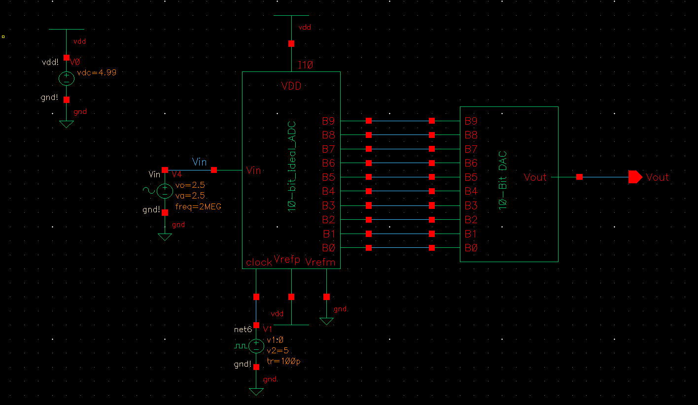
- Open and simulate the ADC to DAC schematic
- Backup all lab files
completed in the lab and prelab
Prelab
The first thing we do is
downlaad our lab2.zip file into our Desktop and upload into CMOSedu
directory.
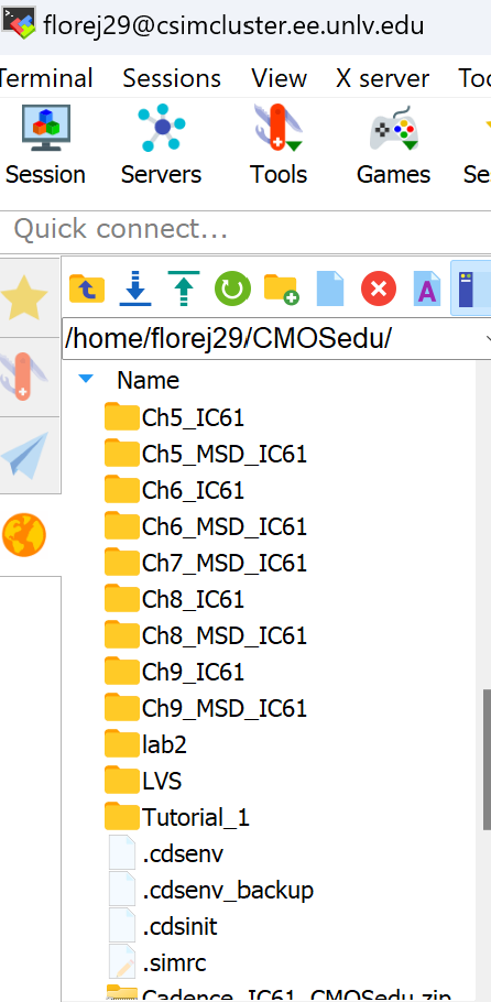
We then unzip in this
current directory, and we should see "lab2" file as seen below:
We
then have to DEFINE this file in our cds.lib file as follows:
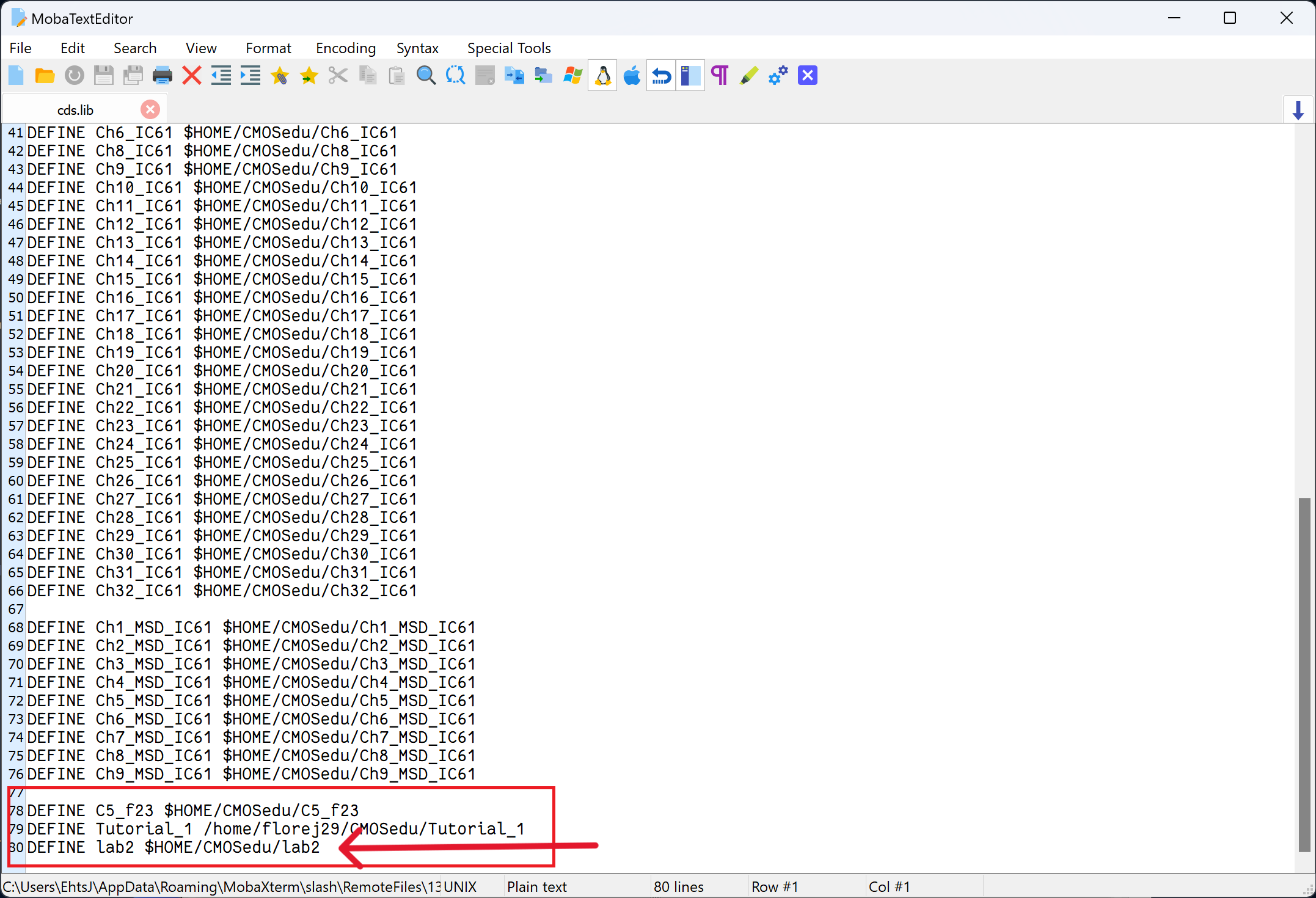
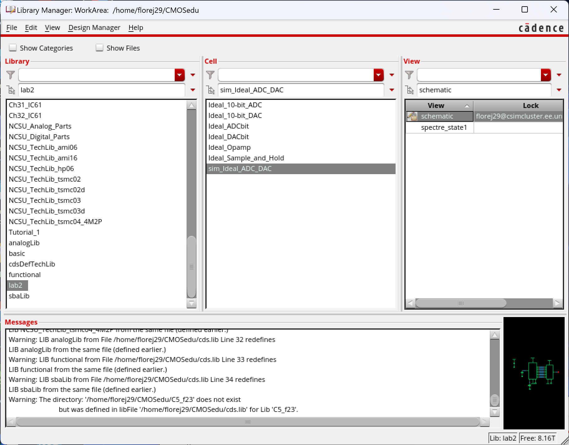
Now we can
proceed to opening up the shematic and simulation as mentioned in the
pre-lab description:
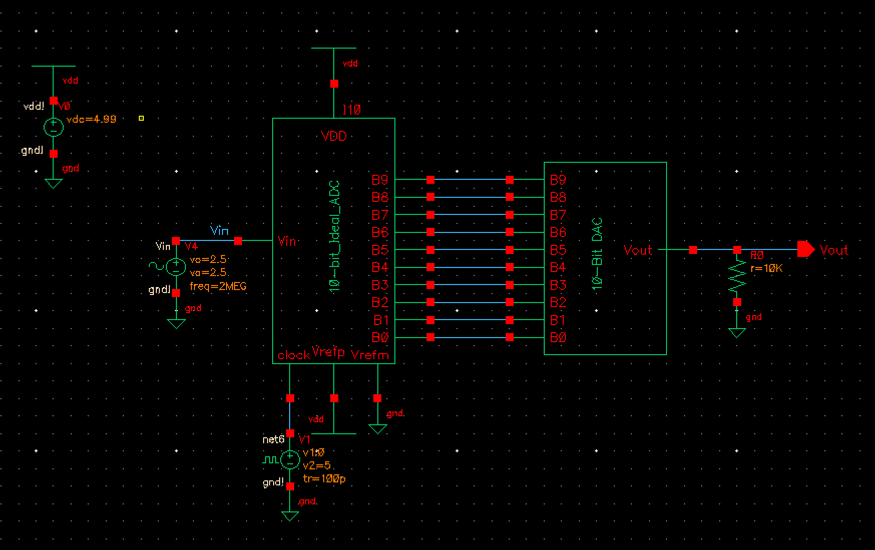
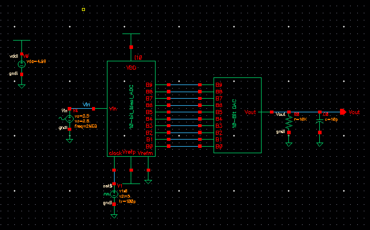
Opening the schematic are running a transient simulation :
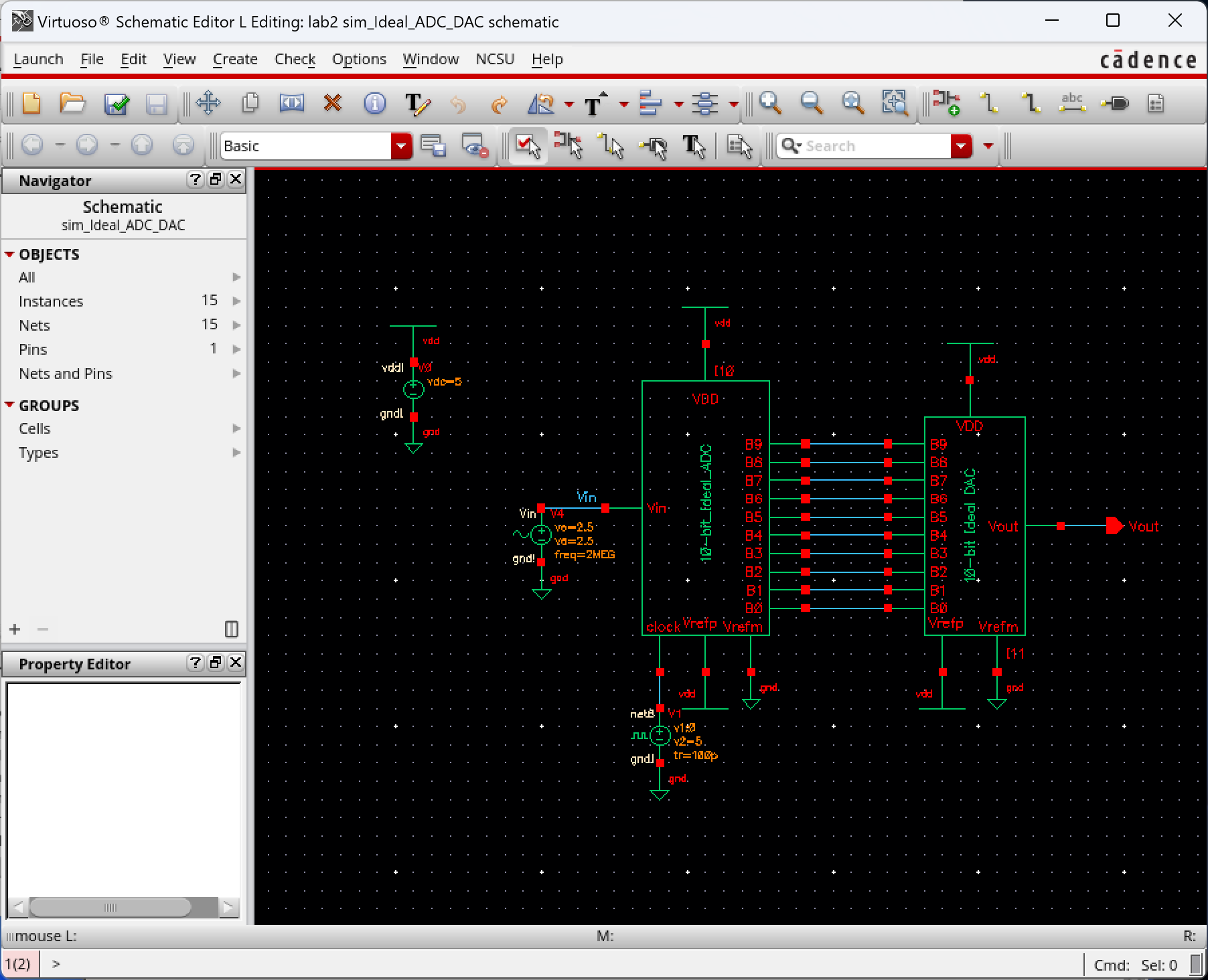
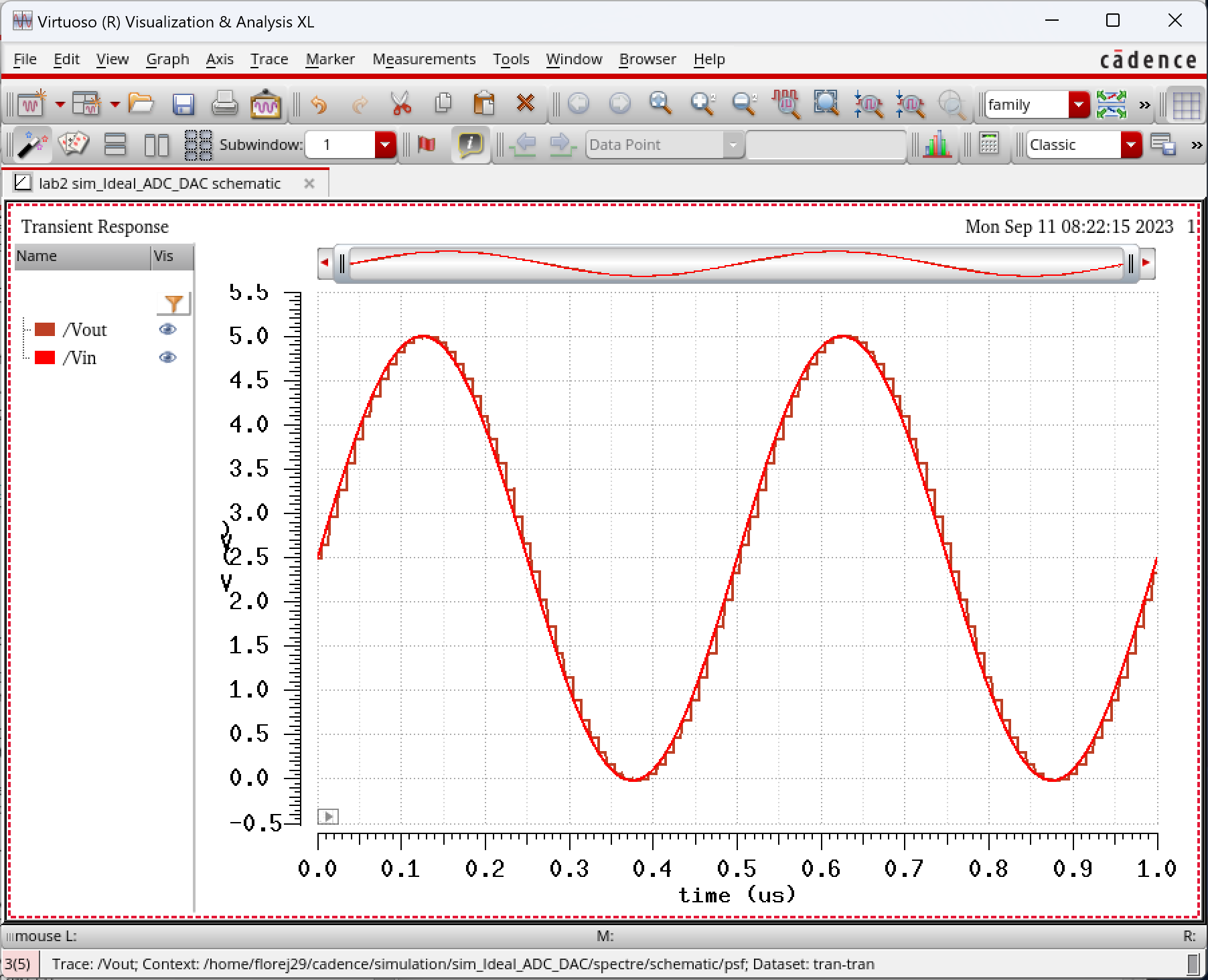
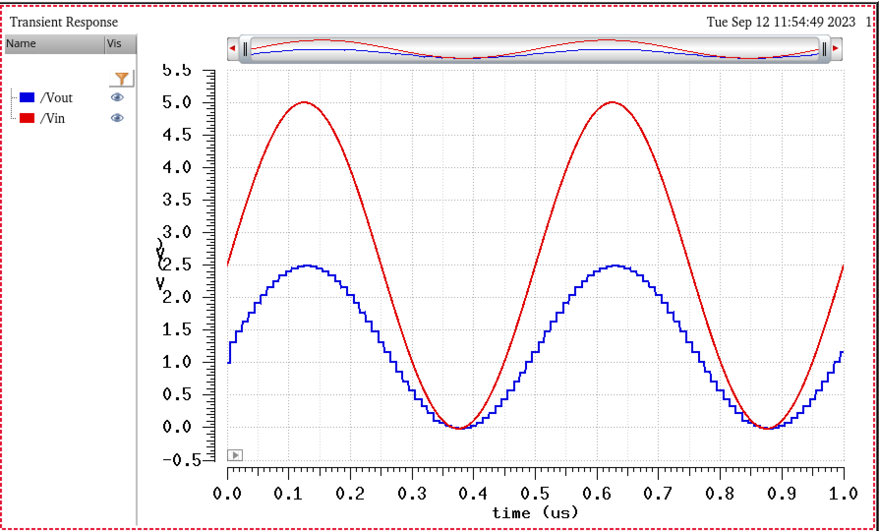
In
the simulation aboce we can notice the sinesodial wave input and a
sinesodial wave output made of pulses. From my understanding, this
output is made this way due to a capacitor placed in parallel with the
output, and having a switch cylce on and off, sampling the
voltage at the point in time when the switch closes. I believe this
creates the step looking sinesodial waveform seen above. This allows
for the system be able to differ from Most Significant Bits (MSB) and
Least Significant Bits (LSB).
How? Well lets take the
simulation for example. The voltage input ranges from 0V minimum to 5V
maximum. The full voltage range will coded or mapped to 10-bit binary
number that we have in our example (i.e .B[9:0]), Each place will
obviously be represented by a 0 or 1. In our case we have 10-bits so we
have a total of 2^10 (= 1024) binary numbers.
With this we can calculate the resolution of the ADC:
This gives us the
resolution of the ADC, or the minimum amount of voltage required to
change the output of the ADC.
So
as an example, lets say the signal amplitude is at 0V, then the digital
mapped number will all zero's (00_0000_0000). It will be all zero's for
the range 0-4.88mV. For voltages from 4.88-9.76mV, the output digital
number will be 00_0000_0001. This pattern continues up into the last or
most significant bit. To emphasize this, I will provide a simulation
showing the step sizes in more detail. See figure below:
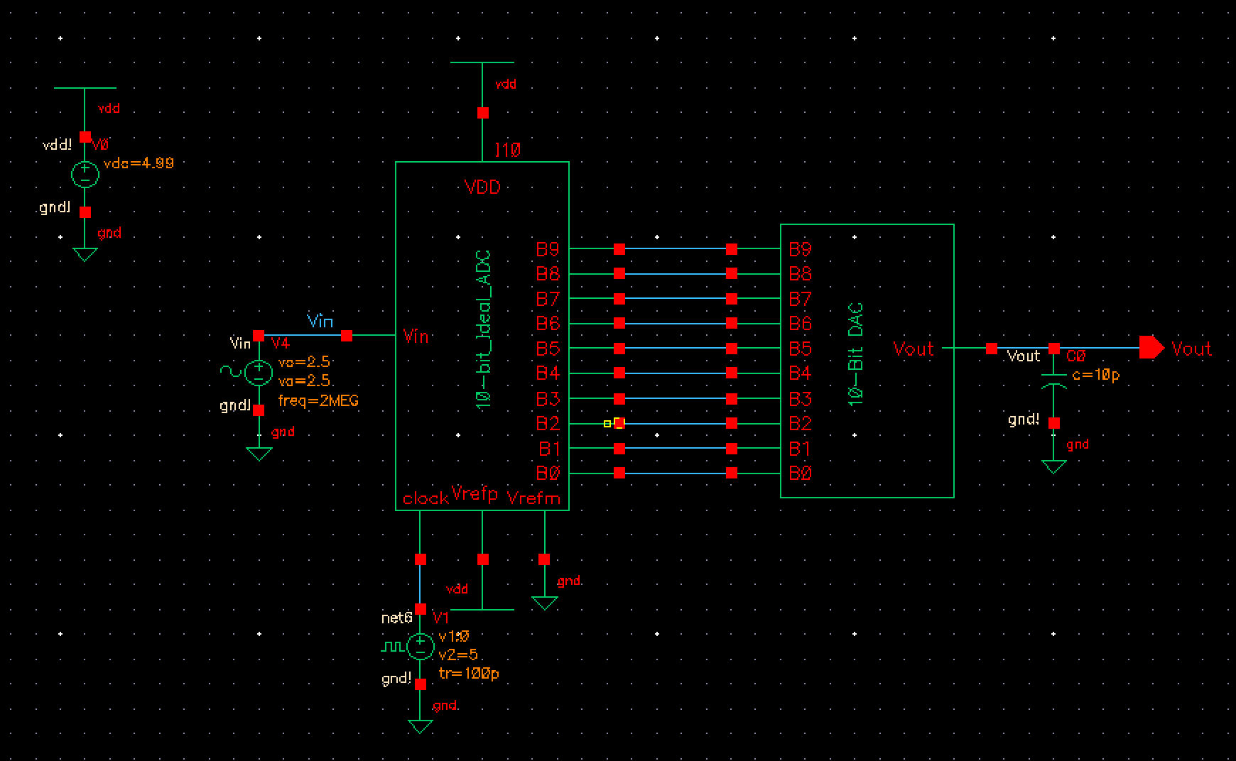
For
this simulation I simply changed the voltage amplitude into a smaller
value (10mv amplitude), and with an offset of 10mv as well, in
order to have the step sizes bigger, and its easier to see rather than
the simulation above:
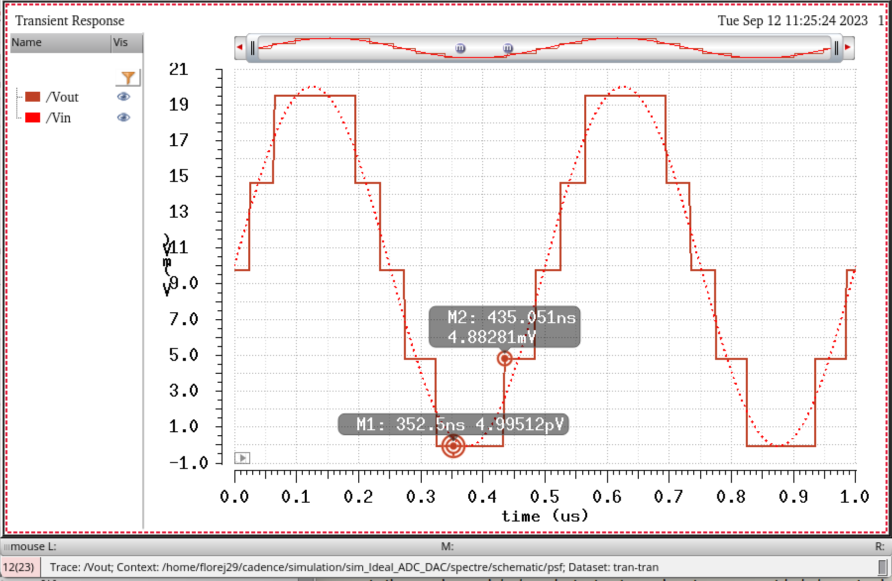
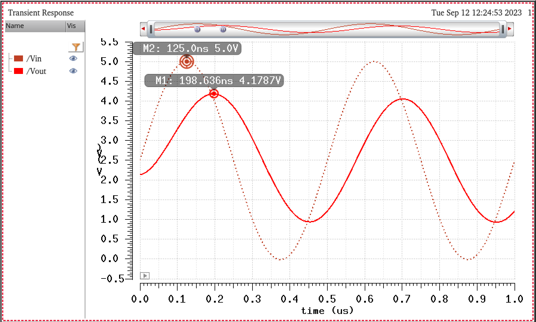
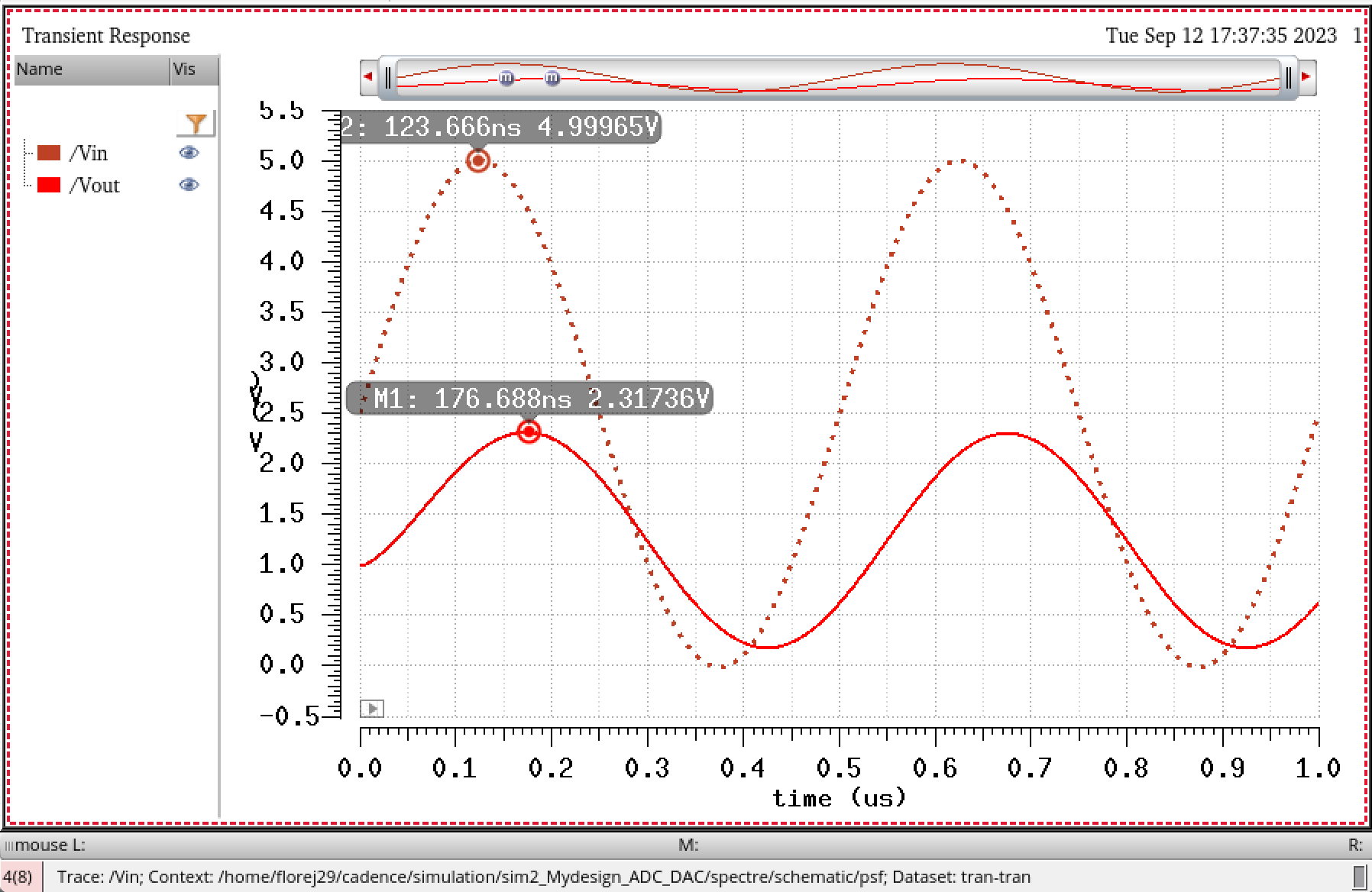
From
the markers placed in the simulation above, you can also verify that
the minimum voltage for a change in the ADC's output ,B[9:0], is
4.88mV. At every new step, the bit increases.
Lab Objectives
-
Understand
how DAC and ADC
works
- We'll use n-well resistors to implement a 10-bit DAC
- Backup all lab
files completed in the lab and prelab
Lab
Designing
Our Own 10-bit DAC Narritive
First
task during this lab was to design a 10-bit DAC with 10k resistors,
similar to the prelab, but designing it as the picture provided above
in the pre-lab section. Below you will find the steps I took to make
this 10-bit DAC.
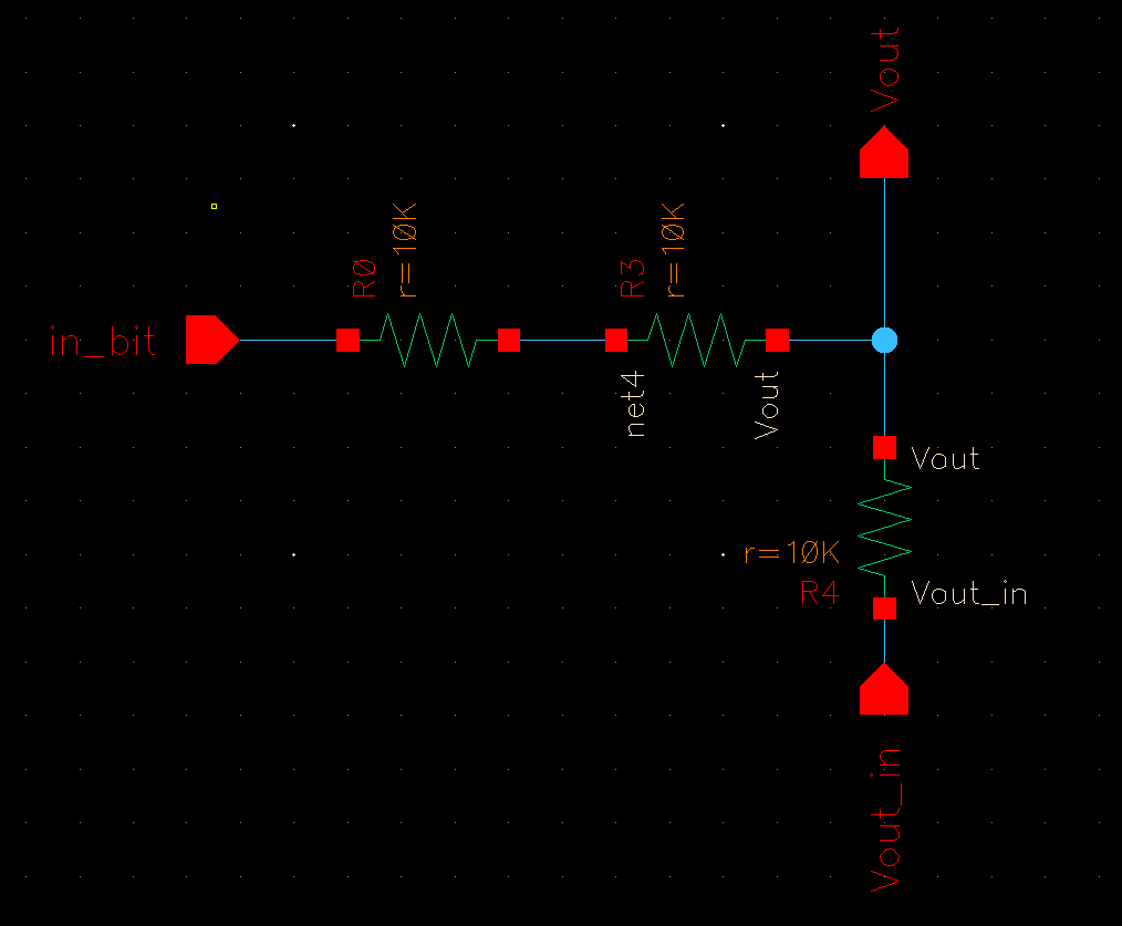
For
starters, we make the DAC bit, which is a single voltage divider with
two resistors in series to compensate for "2R":
We then make
this into a symbol so we can implement 10 of these into our DAC
schematic as follows:
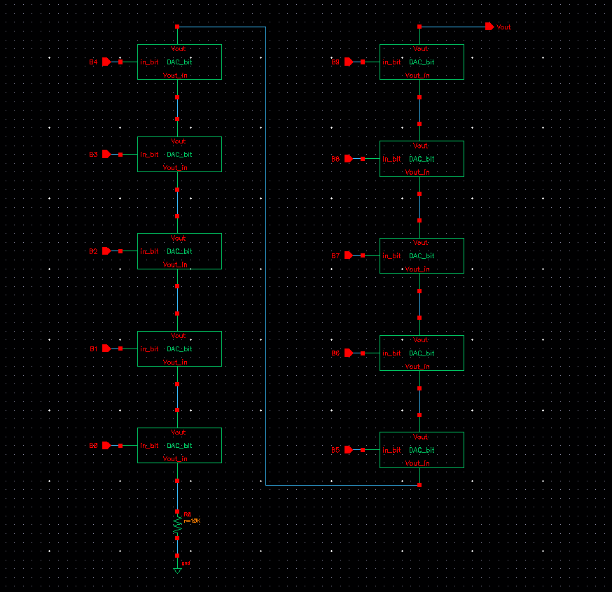
After
drawing this 10-bit DAC schematic, we once again make another symbol
for this drawing now so we can use it into another file where we will
simulate and test that it works just like the ideal version in the
pre-lab. You can see the symbol in the picture below, already connected
within the circuit ready for simulation.
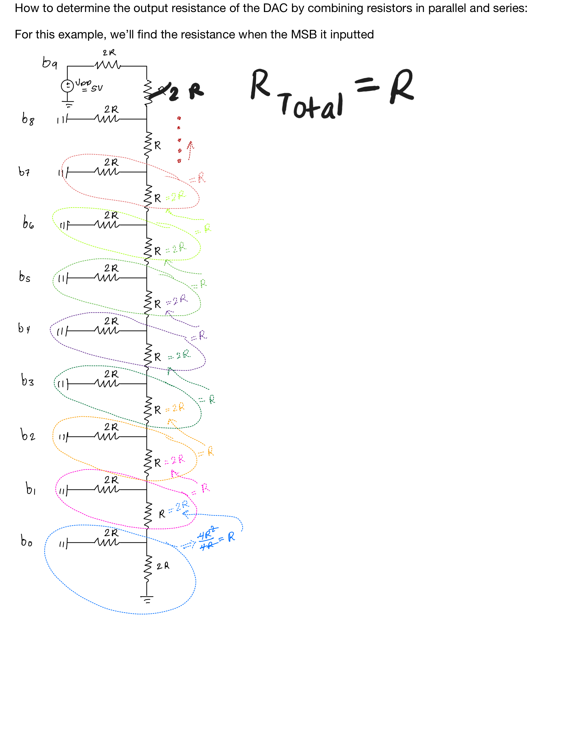
Resistance
of 10-bit DAC
Once
done with this design we were asked to included how to find the DAC
resistance, so heres a small example working out the DAC's output
resistance. Note that through combining resistors in parallel and
series, the output resistance simplifies to R:
Delay
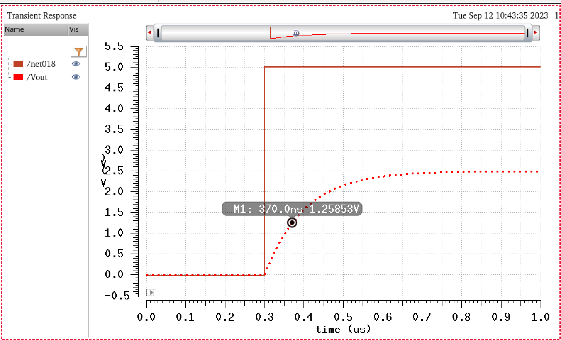
When Driving a Load
To
predict the time delay the DAC will have when driving a 10pF capacitive
load. To find this time delay, we will use the equation:
td
= 0.7RC
Here
our R value is equal to 10k ohms, which is the value of the DAC
resitance. The capacitance is the capaitors value, which is given in
the lab, i.e 10pF.
td =
(10k)(10pF) = 70ns
In
the image below, you can verify from the simulation that the time it
takes for the capacitor to charge to half its peak voltage
(2.5V),
it takes about 70 ns. Note that for this simulation my pulse voltage
source has a 0.3us delay, so from the time the voltage source turns on
at (0.3us) to the time the capacitor reaches 1.25V (370ns = 0.370us) is
equal to 70ns.
Simulations
to Verify Design Functionality
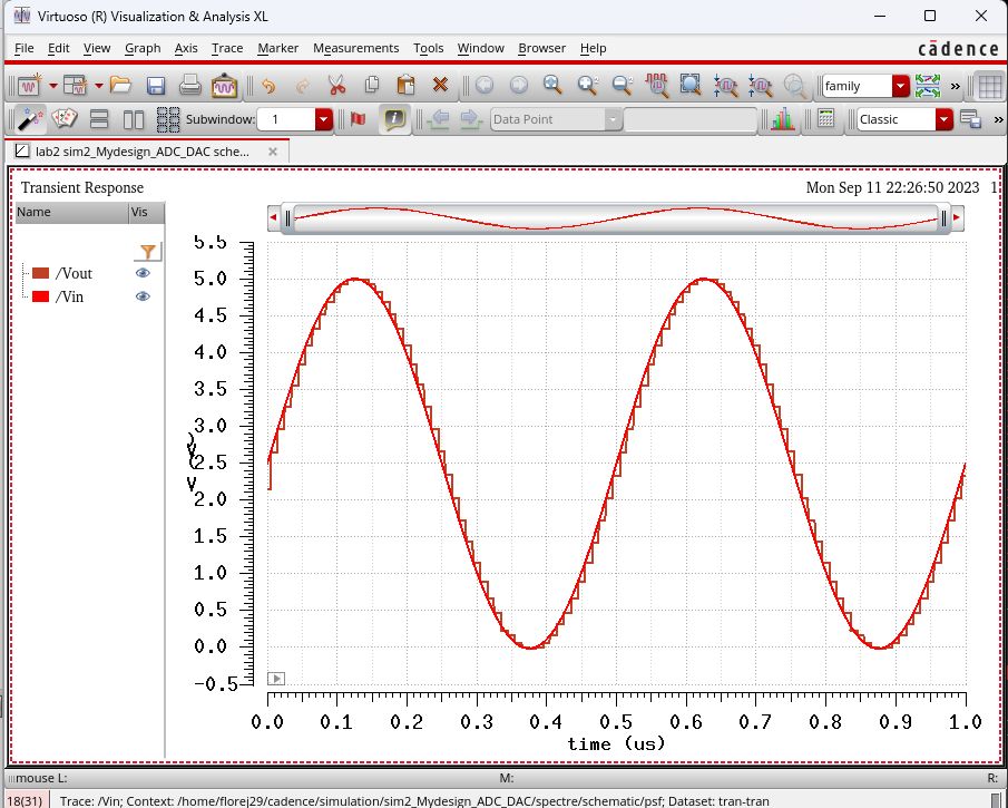
Going
back to the DAC, below you will find the simulation verifying that my
design version works just like the ideal pre-lab example. This simulation is with no load:
-Driving
a 10k Resitive Load
Now lets apply have the DAC drive 10k resistive load:
You
will notice that Vout is now half the voltage of Vin. This is due to
the DAC also having a 10k resistance. So when we connect a 10k resistor
in series with the DAC, we get a voltage divider.
-Driving
a 10pF Capacitor
Driving a 10pF capacitive load:
As
seen from the image above we can see that Vout lags the input voltage
due to the capacitor.We should also note that the output voltage has a
DC offset of 1V compared to the results from above. To confirm the
result of Vout, we can find the trasnfer function of this circuit,
which is a voltage divider, and find the magnitude to be 3.1, plus the
offset of 1V yields the above simulation results.
Similary to find
the time delay or phase shift of these results, we can find the phase
shift of the transfer function. Once we find the phase shift, which is
about -51.5 degrees we can derive the time delay by the following
equation: time delay =
(phaseshift/360)(1/frequency) = 0.07us
Driving
a R/C Load
Finally,
we look at a load with a resistor and capacitor:
Similary,
for this simulation above, you
can see that the output voltage is jus below that of a voltage divider,
due to the capacitor. We also have a slight offset with a lag on the
output.
In a real
circuit the switches seen
above (the outputs of the ADC) are implemented with transistors
(MOSFETs). Discuss what happens
if the resistance of the switches isn't small compared to R.
-
If the resistance of the switches were not not small compared to R, we
would have to re-calculate the circuit since the resistance wouldn't be
2R, but higher due to the resistance in series along with the 2R
resistor.
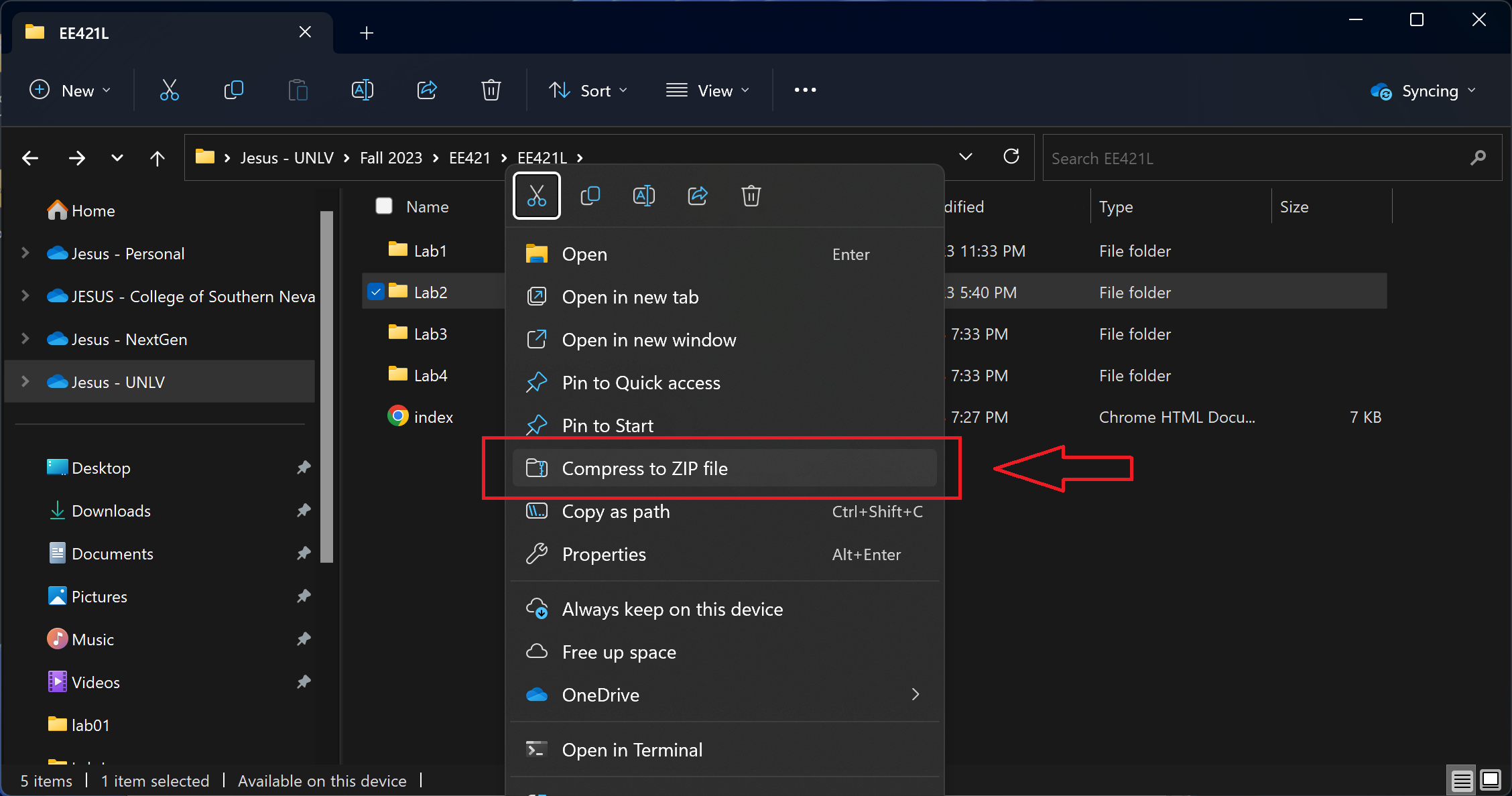
Backing
Up My files
First step to backing up my files are to zip my lab2 folder as seen
below:
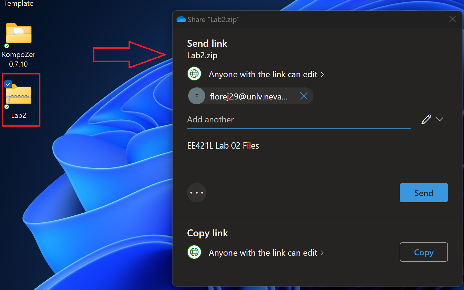
I then
proceed to emailing me this zip file to my student email :)
Return
to florej29 Lab Reports
Return
to Fall 2023 EE421L Student Lab Reports
Return
to Fall 2023 Digital Integrated Circuit Design Laboratory Home Page