
Lab 8 - ECE 421L
Prelab Content
Prior to this lab session, we were tasked with backing up our previous work (as usual) as well as finishing Tutorial 6, in which we learned how to place circuit layouts in a padframe for frabrication. We were also tasked with giving the entire lab document a quick read through in preparation of the actual lab.
Pad Schematic:
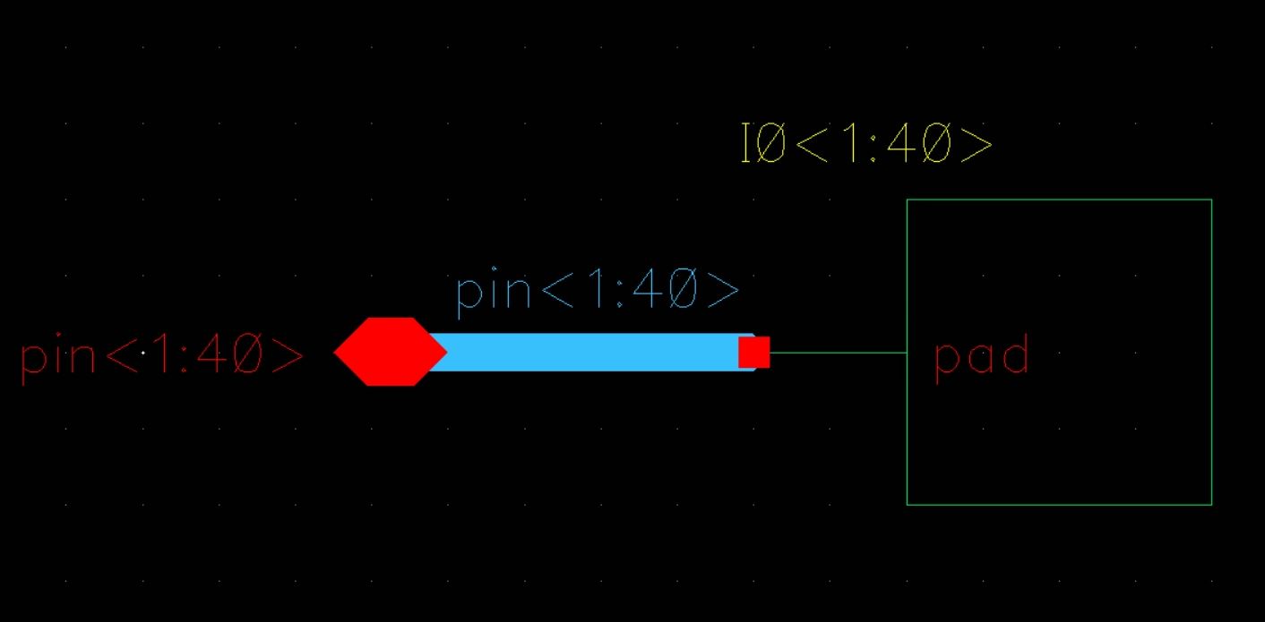
Pad Symbol:

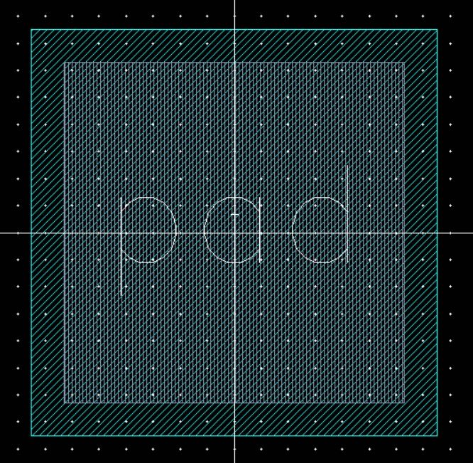
Pad Layout:
Pad Frame Schematic:
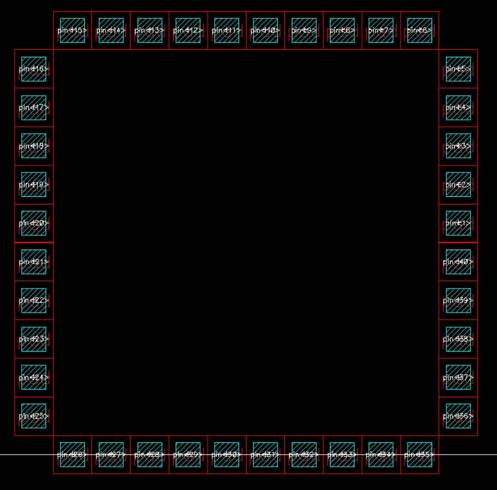
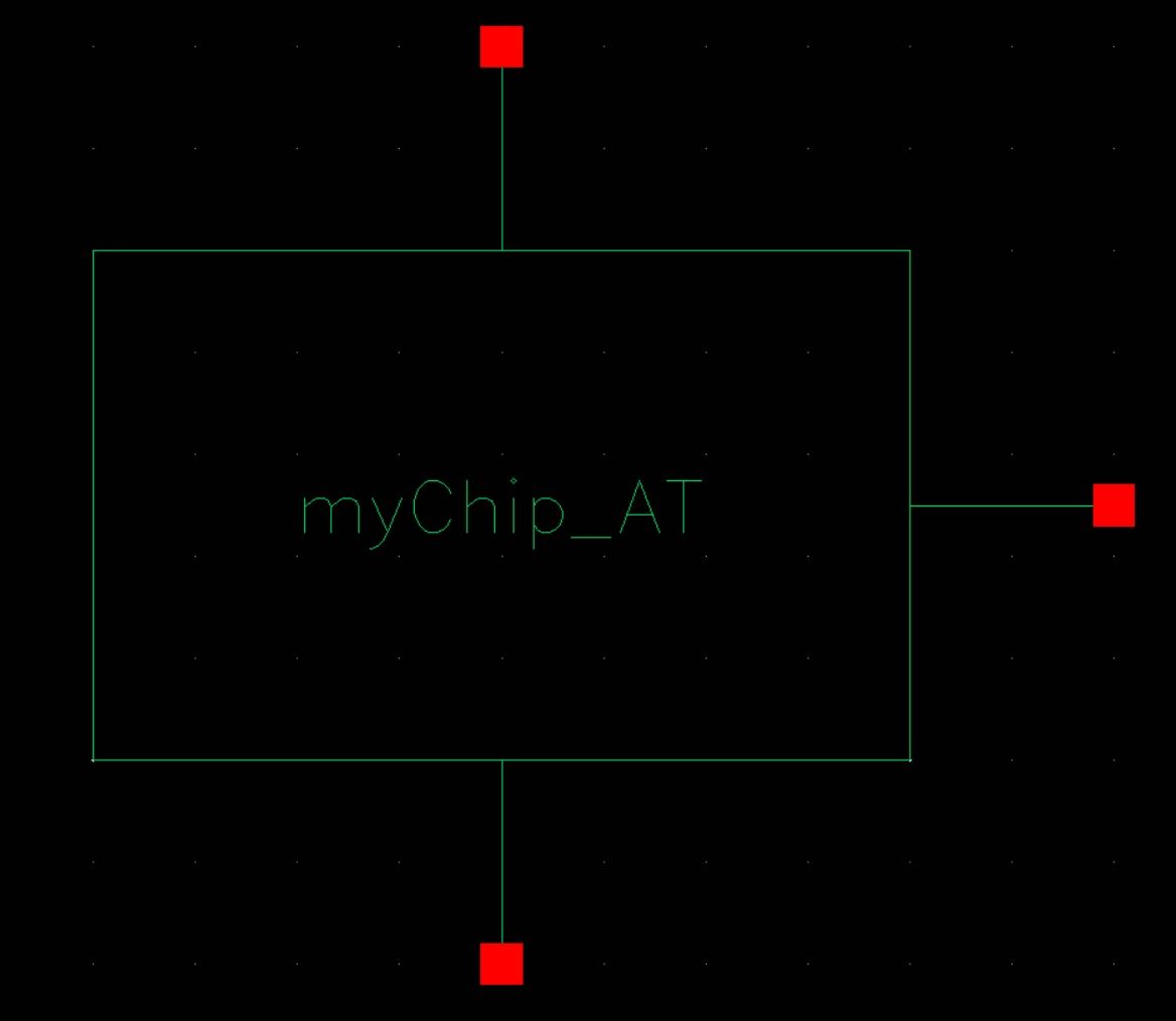
Pad Frame Symbol:

Pad Frame Layout:
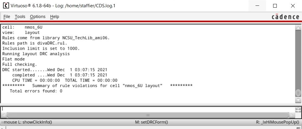
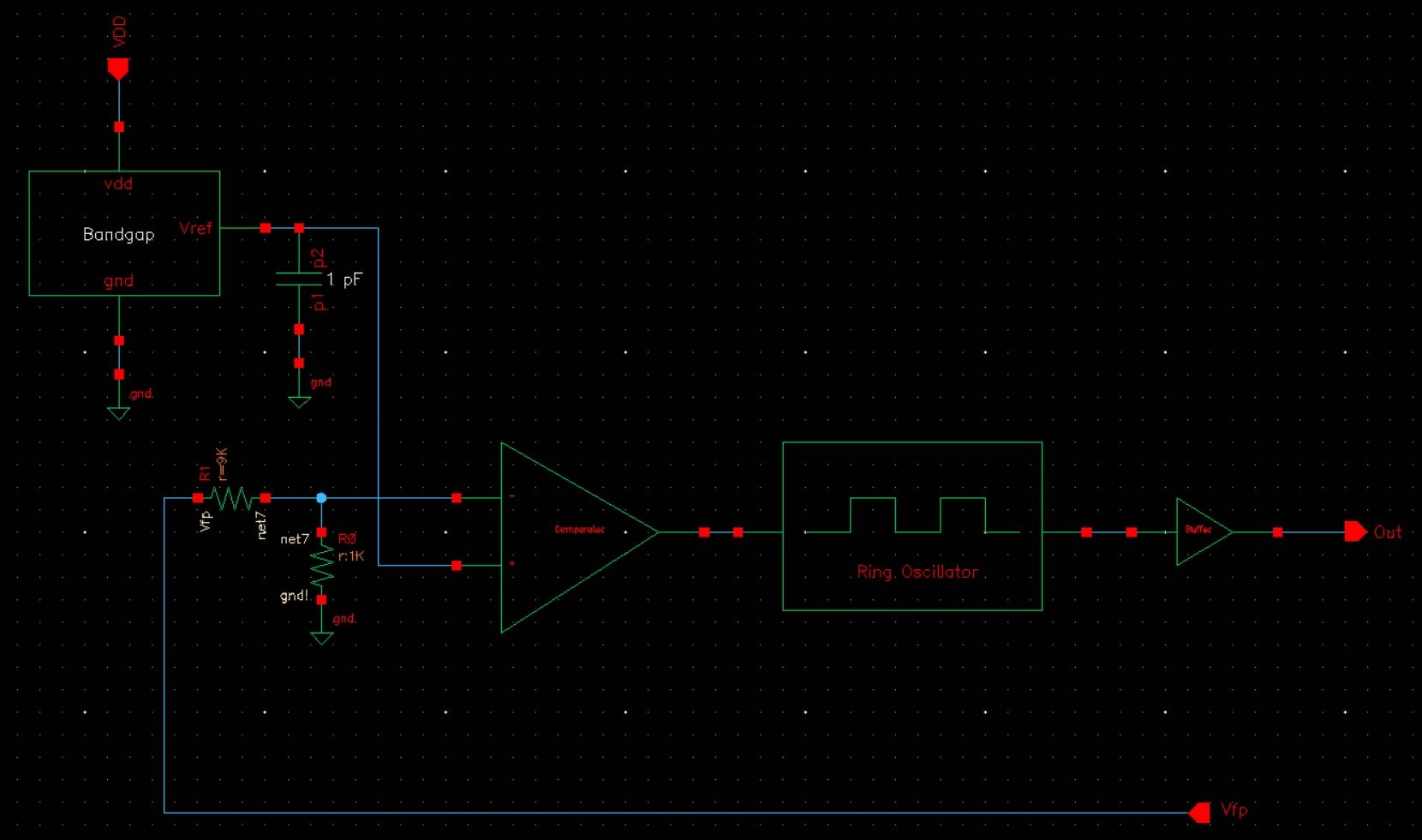
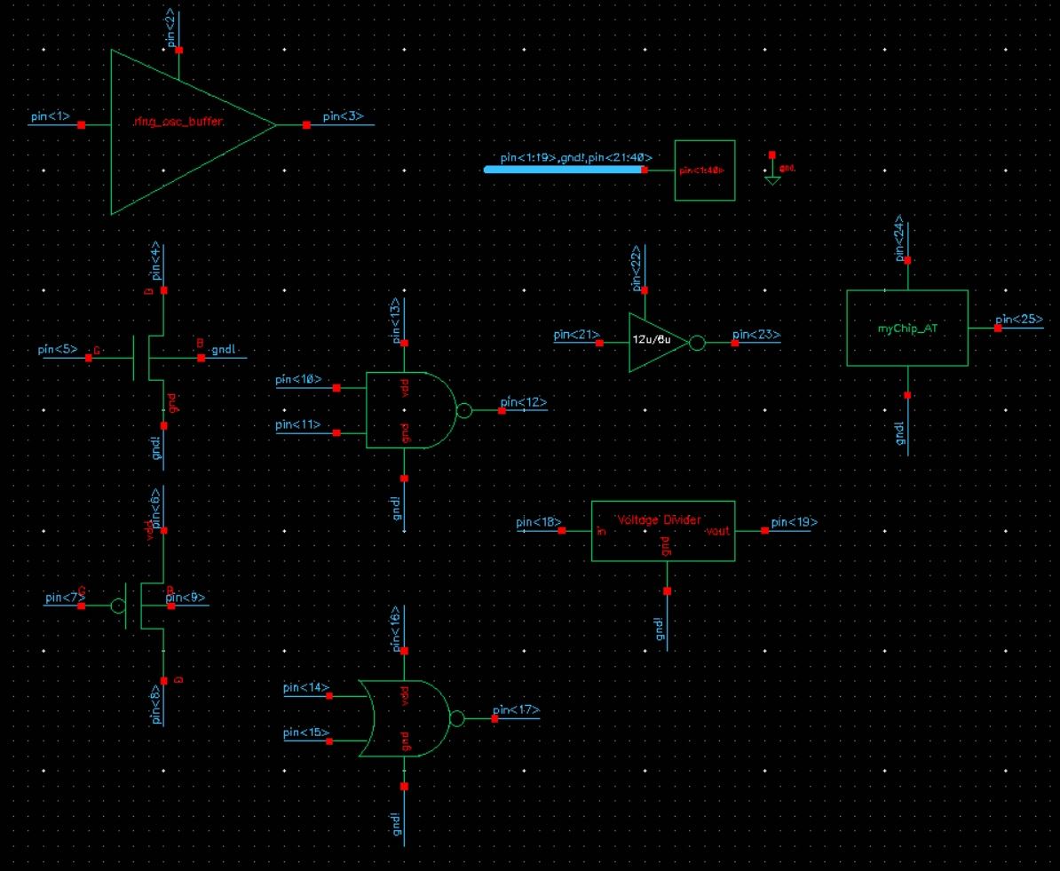
For the main portion of the lab, our group of 3 was tasked with putting several test structures onto a chip. Each test circuit was required to have its own power pin, so that a vdd!-gnd! short in one circuit would not make any of the other circtuits inoperable; however, they did all share a common ground pin (pin 20).
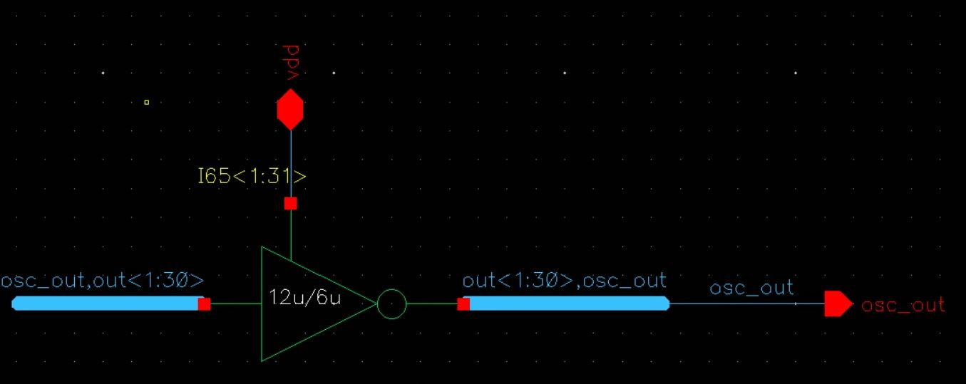
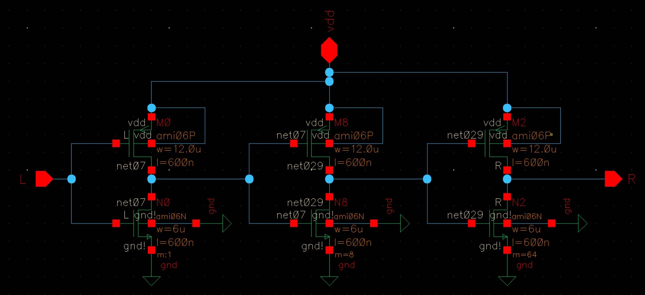
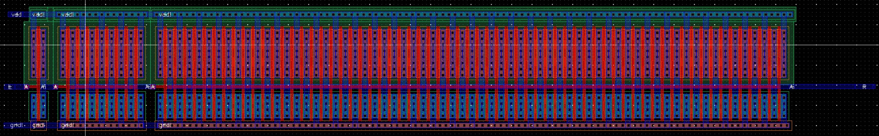
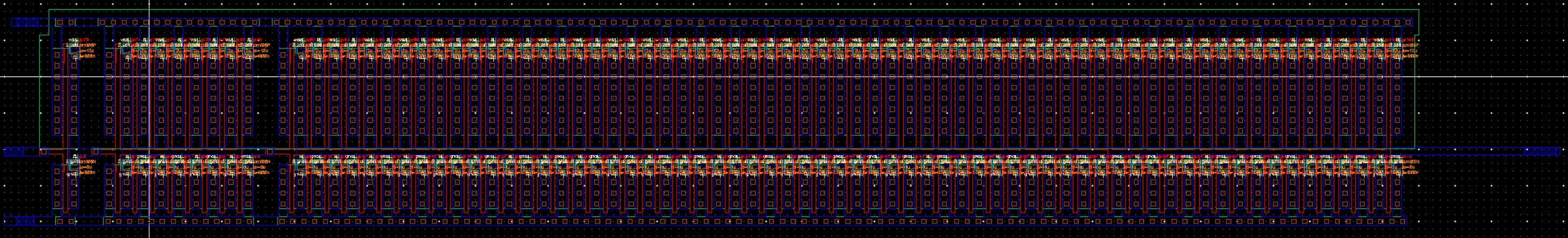
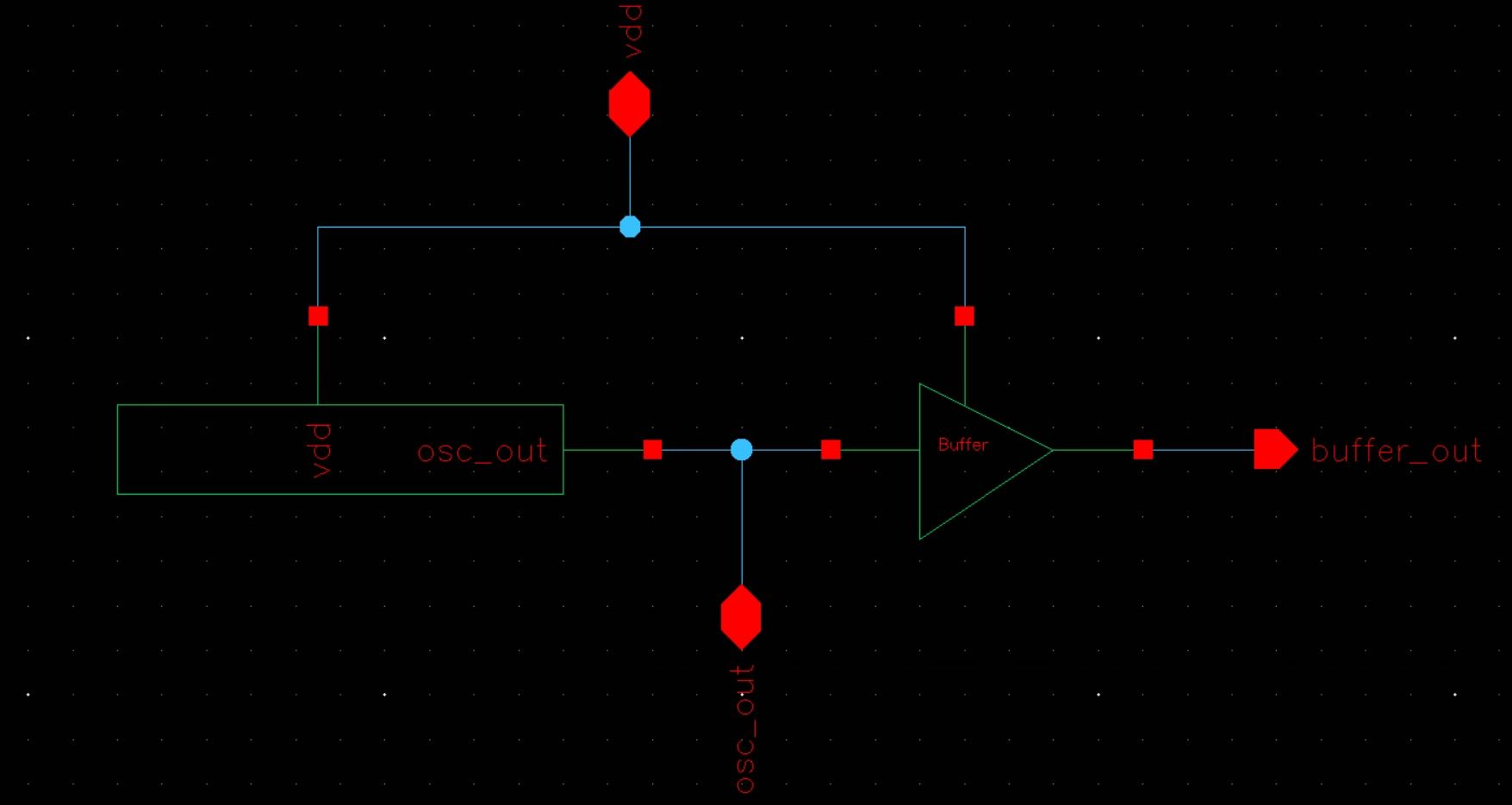
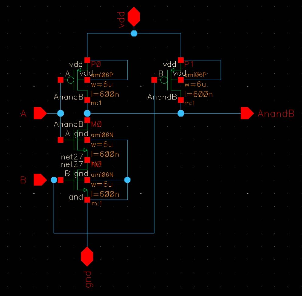
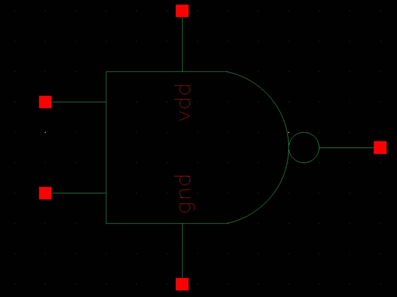
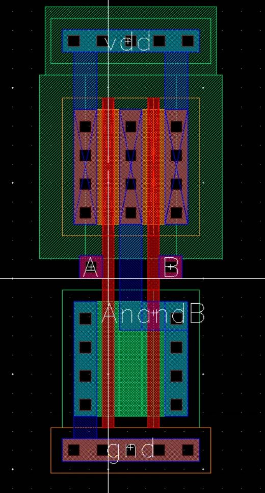
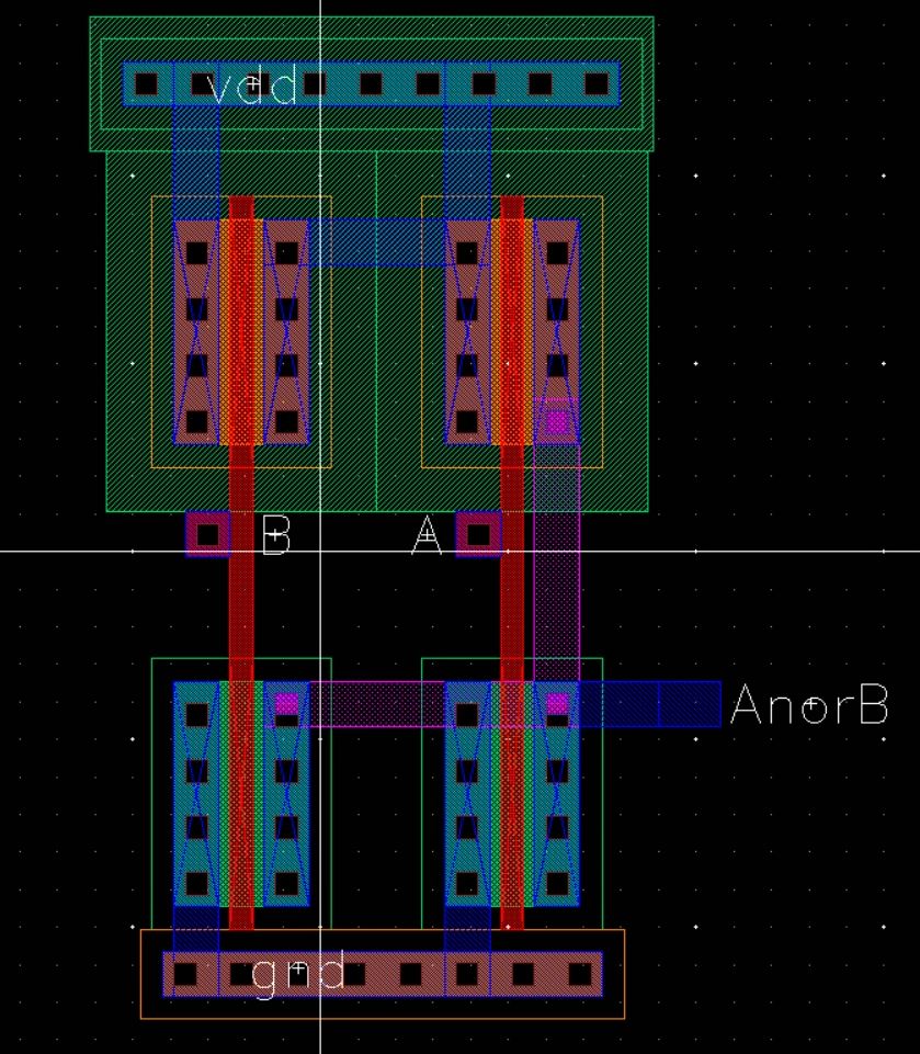
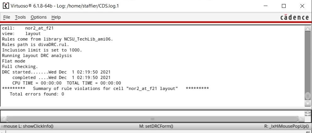
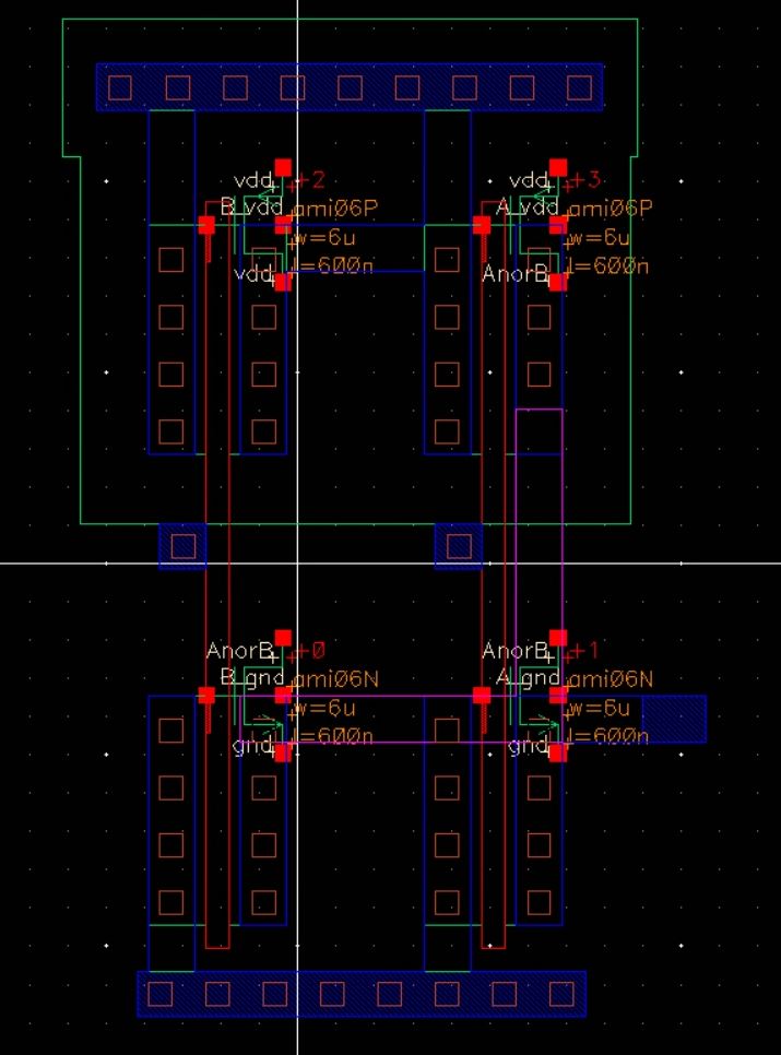
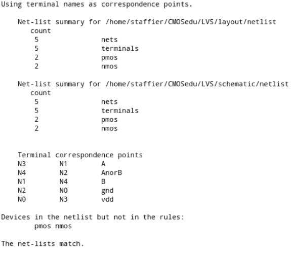
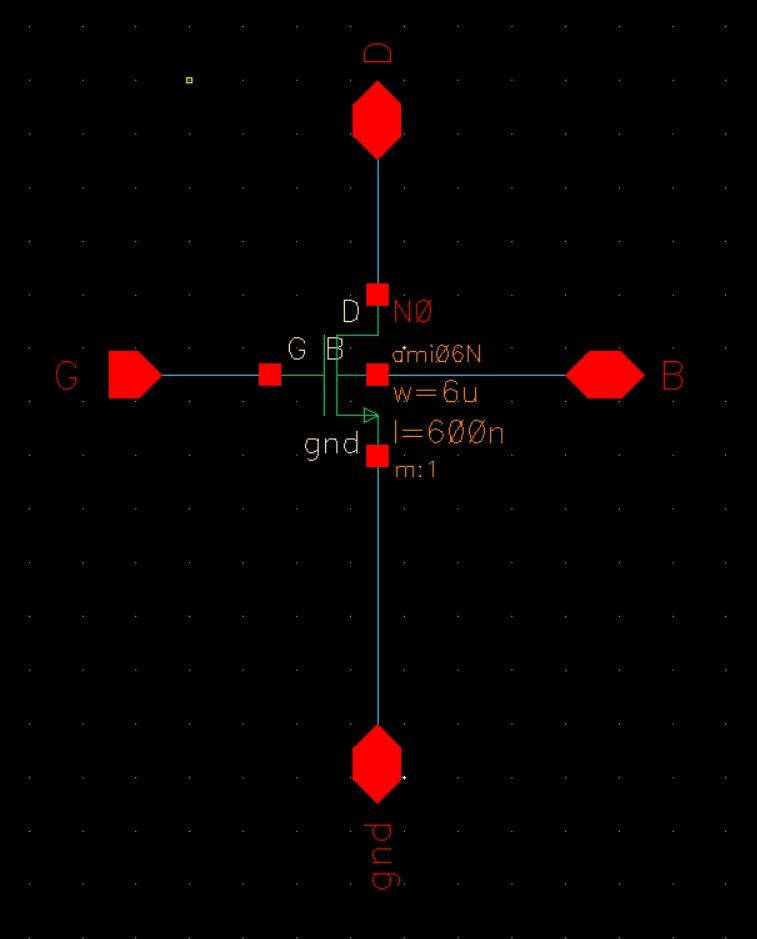
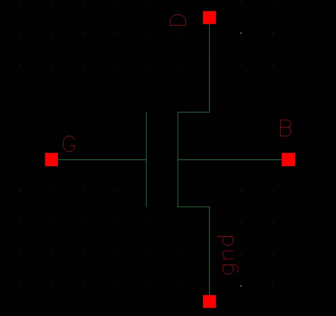
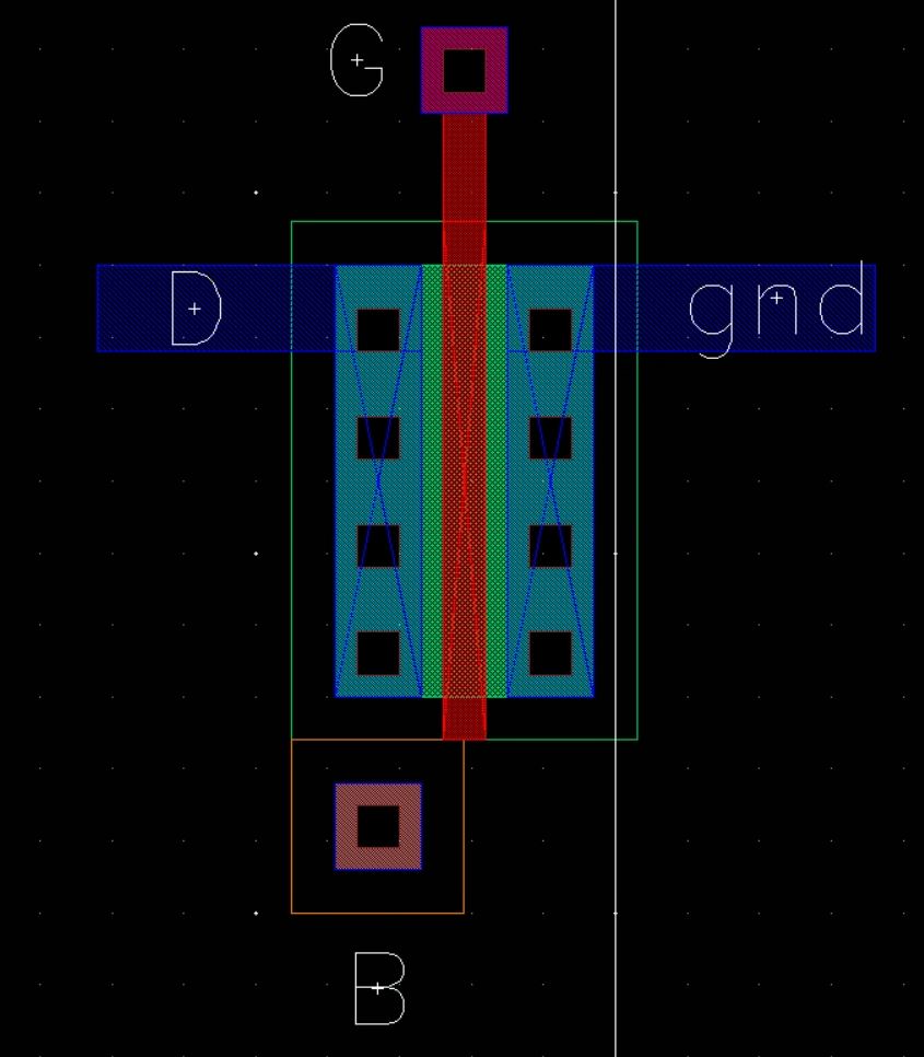
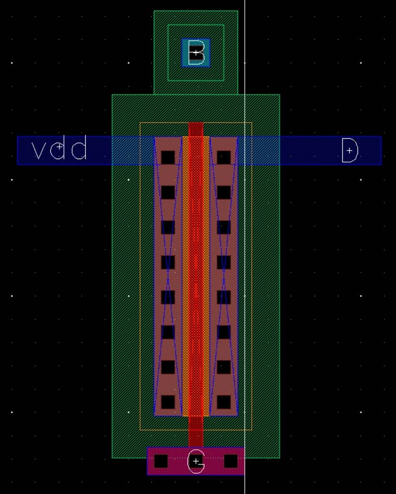
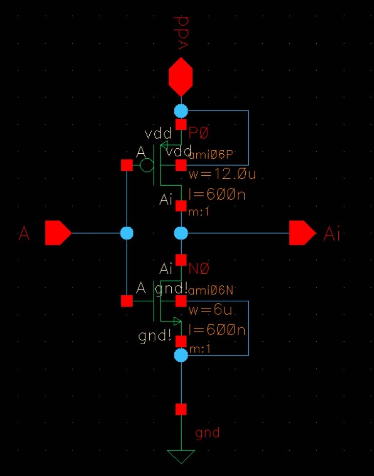
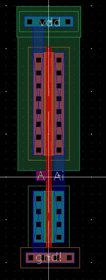
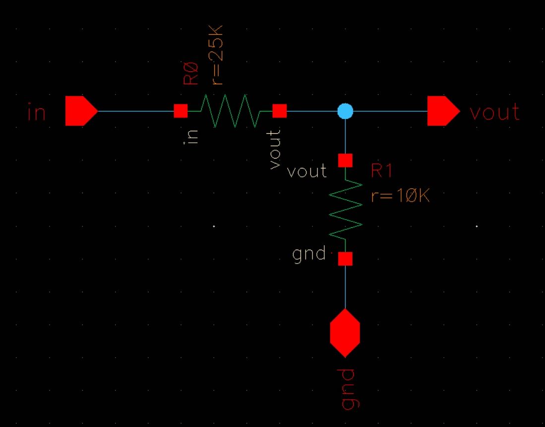
The test structures required are as follows: 31-stage ring oscillator, NAND and NOR gates using 6u/0.6u NMOSs and PMOSs, inverter made with a 6u/0.6u NMOS and 12u/0.6u PMOS, transistors (both PMOS and NMOS) measuring 6u/0.6u, a voltage divider using resistors implemented using the n-well, and at least one course project.


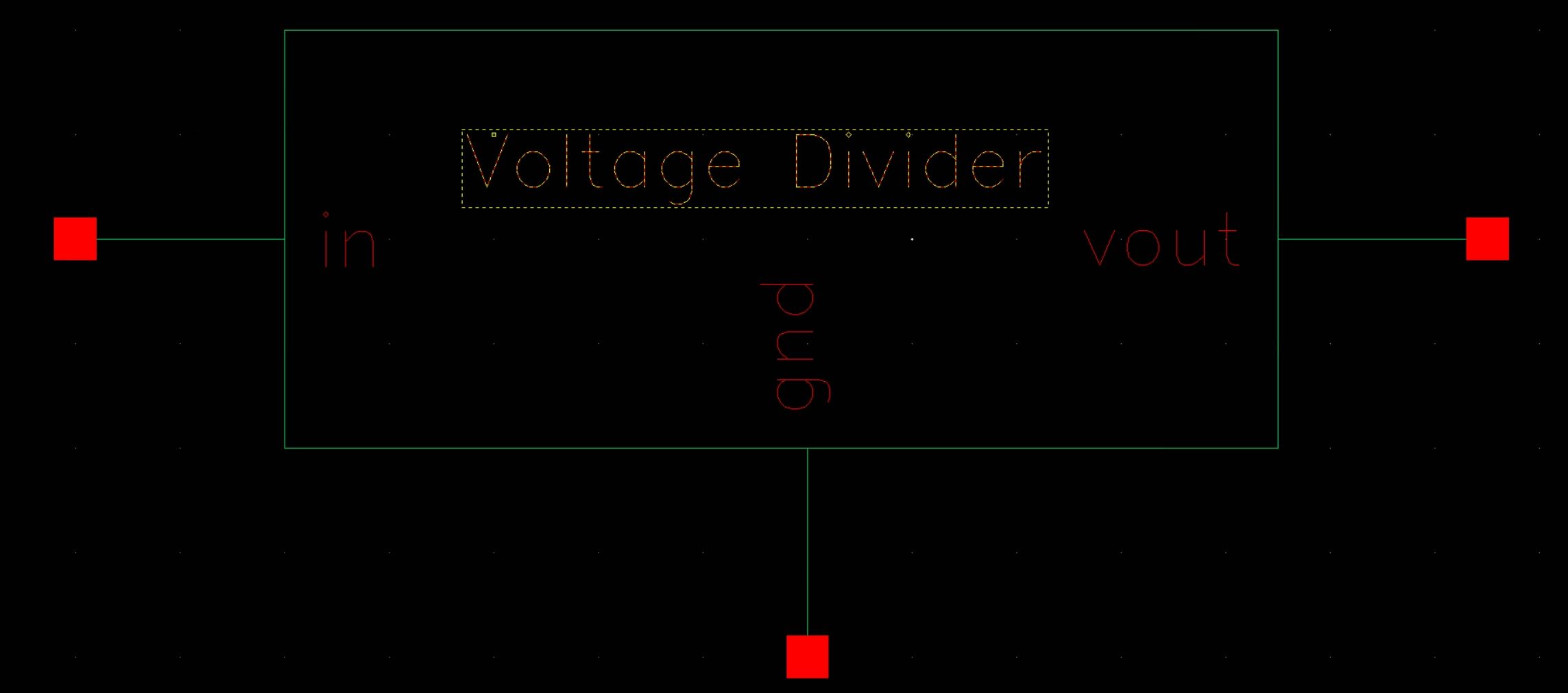
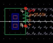
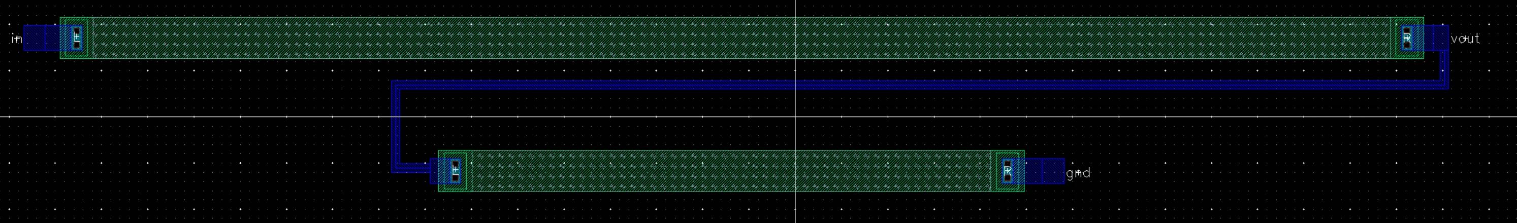
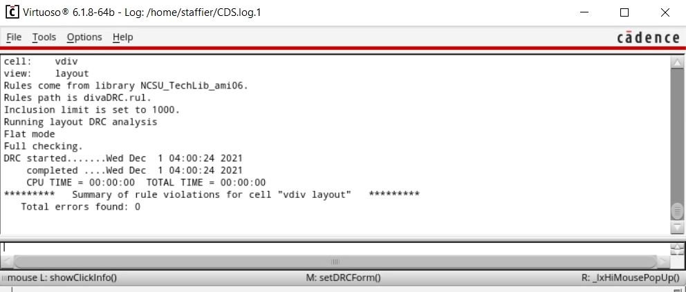
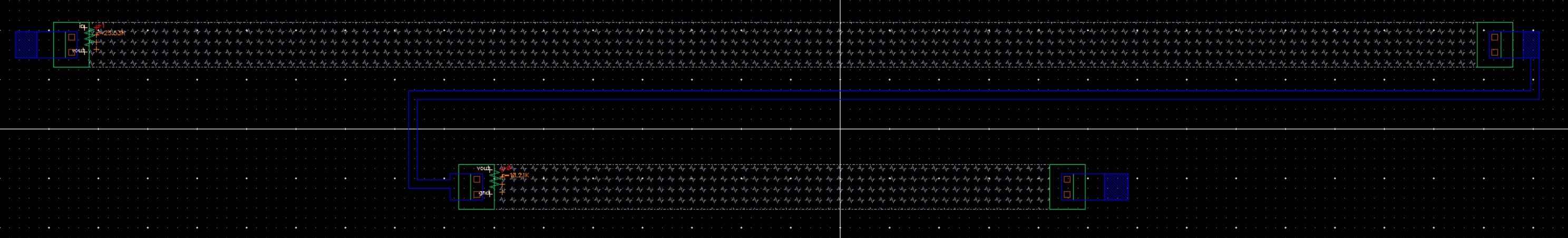
Voltage Divider
Voltage Divider Schematic:
Voltage Divider Symbol:
10K Resistor Layout:
10K Resistor Extracted:
25K Resistor Layout:

25K Resistor Extracted:
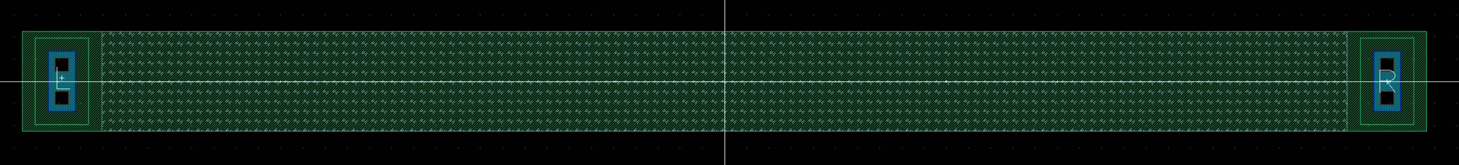
Voltage Divider Layout:
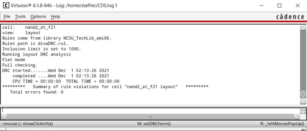
Voltage Divider DRC Clean:
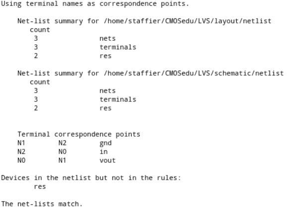
Voltage Divider Extracted:
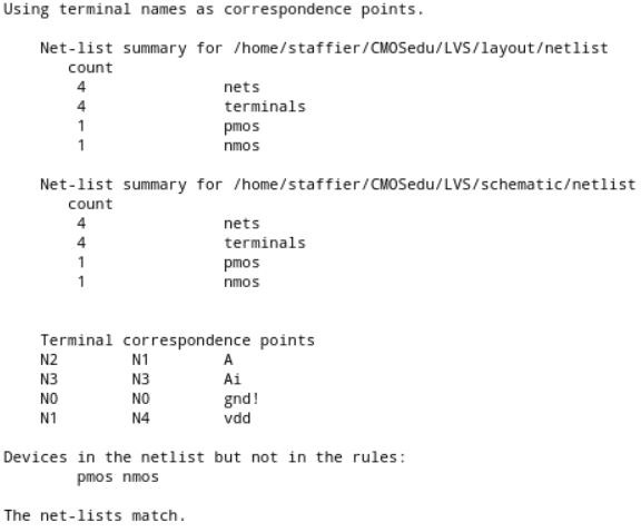
Voltage Divider LVS Clean:
For
the course project, we implemented a design from the lecture portion of
the course, being a switching power supply boost converter. This is a
DC-to-DC power coverter that steps up the voltage from its input.
Course Project Layout:
Course Project DRC Clean:
Course Project Extracted:
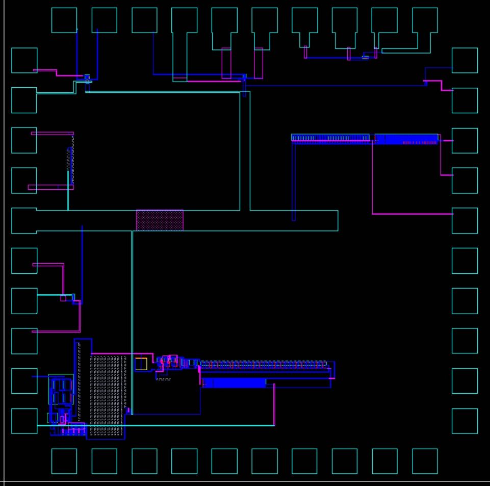
Chip
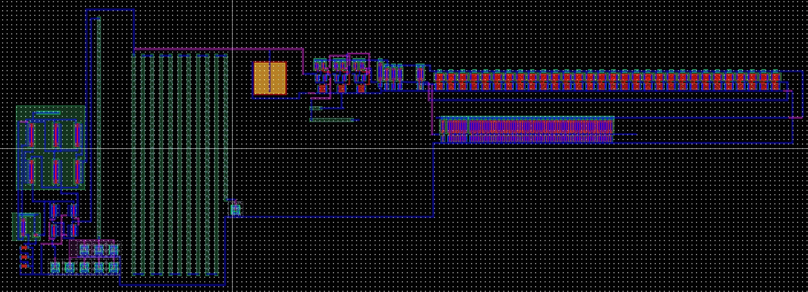
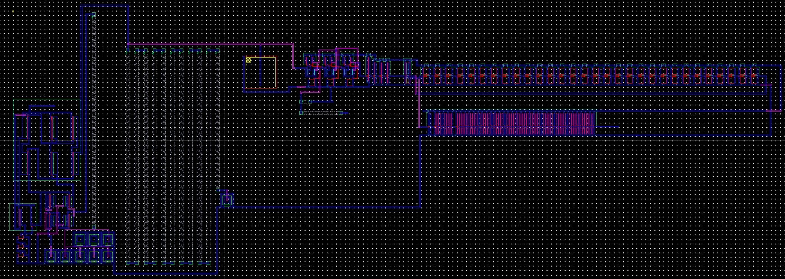
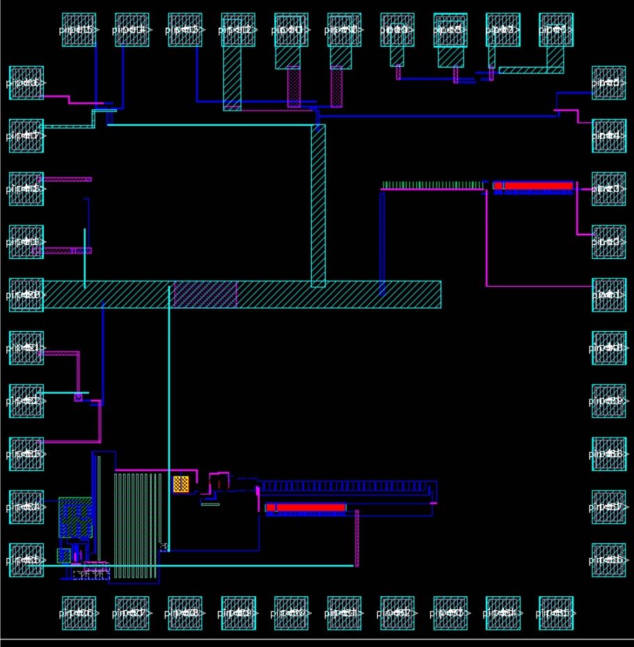
Now for the actual chip itself, we used the pad and padframe that we created in Tutorial 6 in order to set it up. The schematic simply has all of the components with appropriate pins assigned and the layout simply shows each component placed relatively close to the pins that it utilizes, with metal layers to attach the component to either its corresponding pins or the common ground (pin 20).
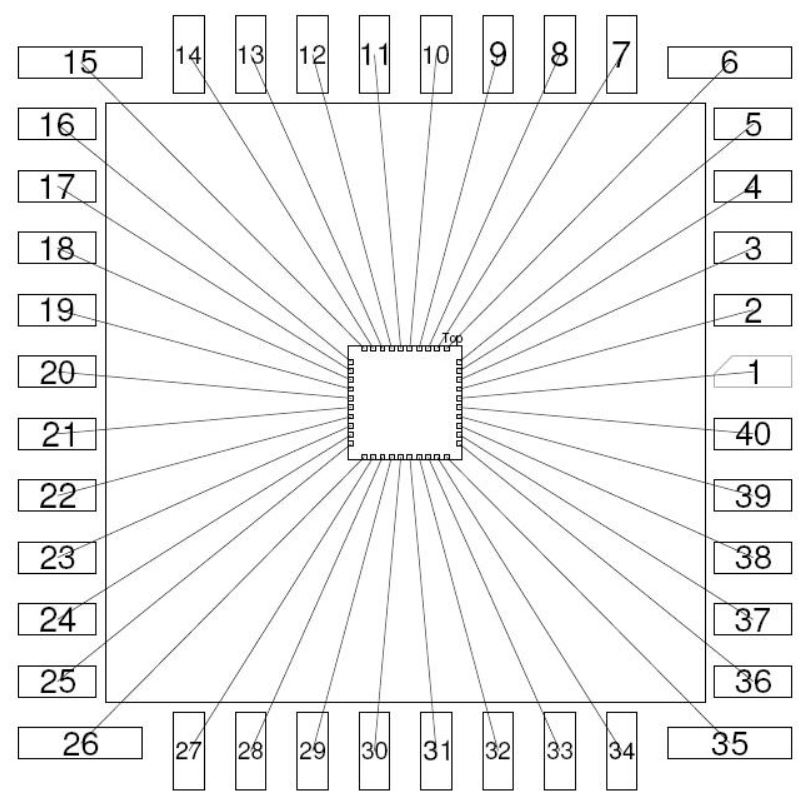
As
the bond pads indicate the pin assignments for the chip, testing the
chip is simple, as all you have to do is SMD solder a wire to the pad
and create the necessary connections to run any of the components. Pin
20 is a common ground for all of the implemented components, and each
component has its own VDD pin that will need to be supplied with power
in order to drive it. The pin assignments correspond to the following
image, and our implementation can be observed after:
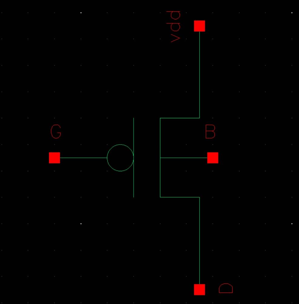
Chip Schematic:
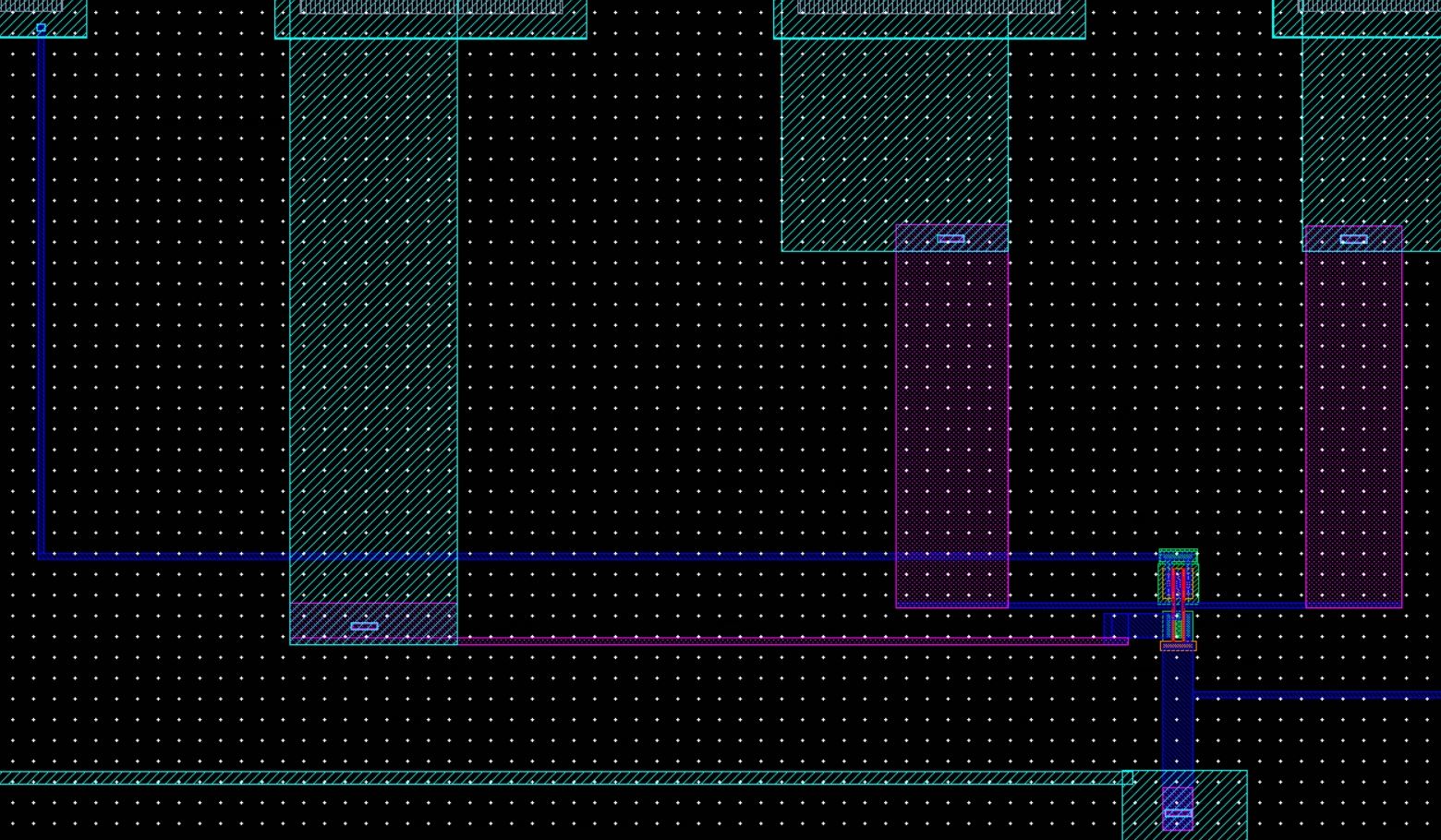
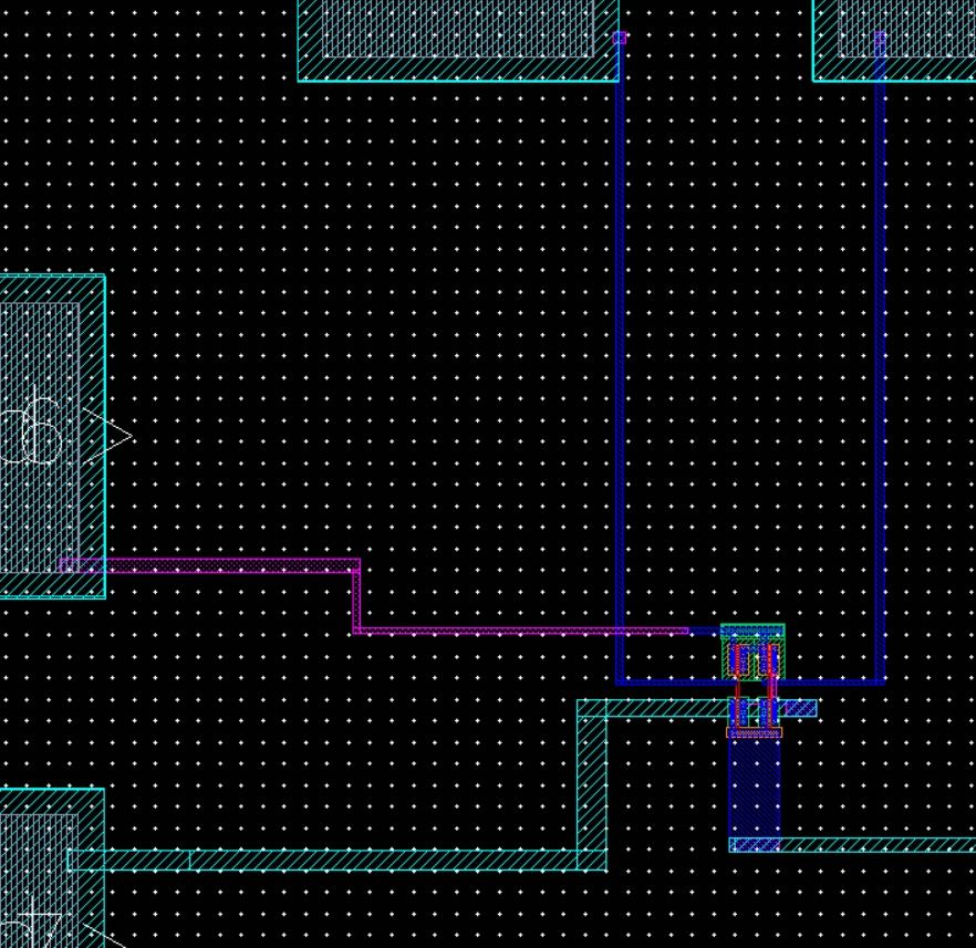
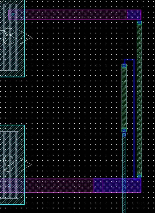
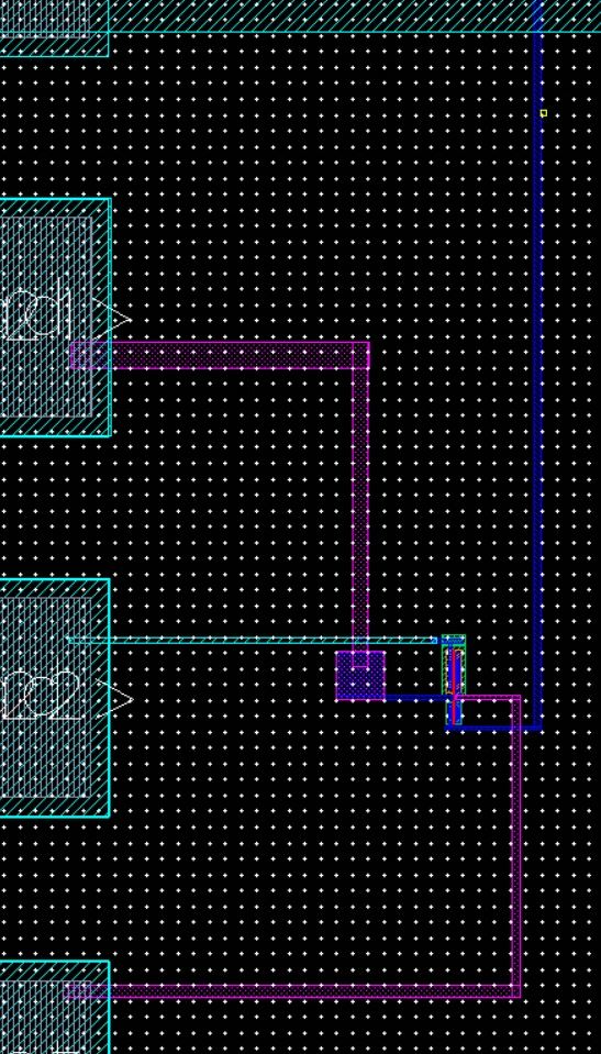
Chip Layout:
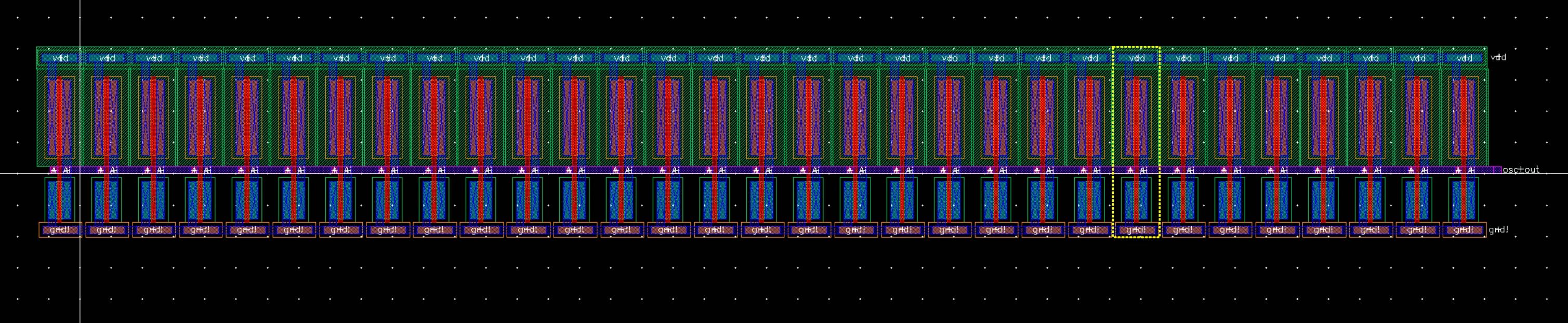
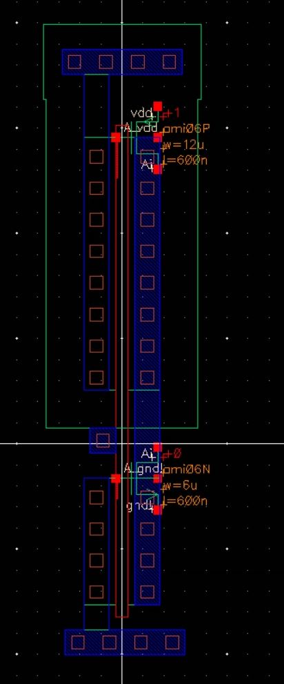
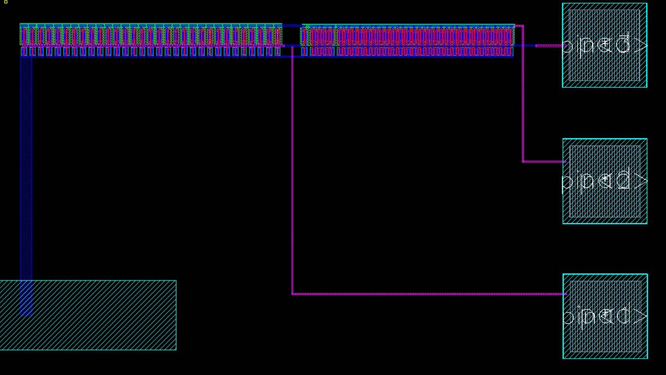
Chip Layout (zoomed into ring oscillator):
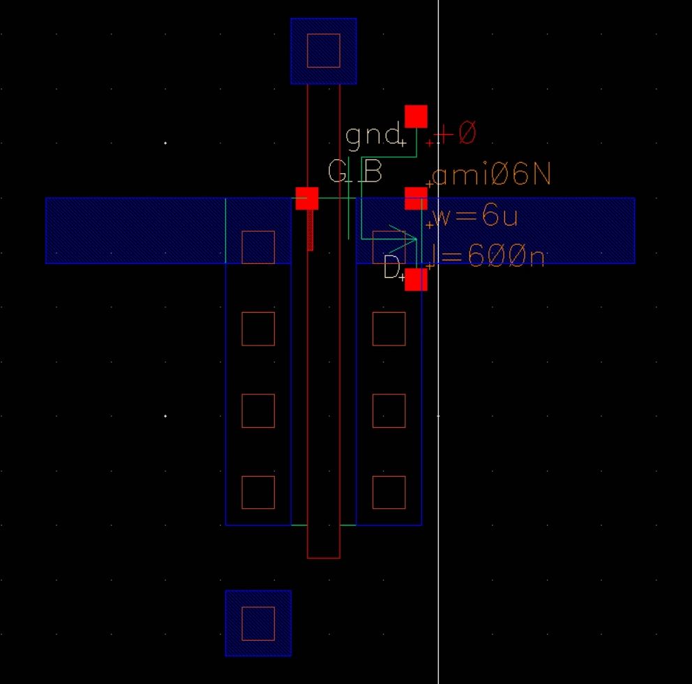
Chip Layout (zoomed into NMOS):
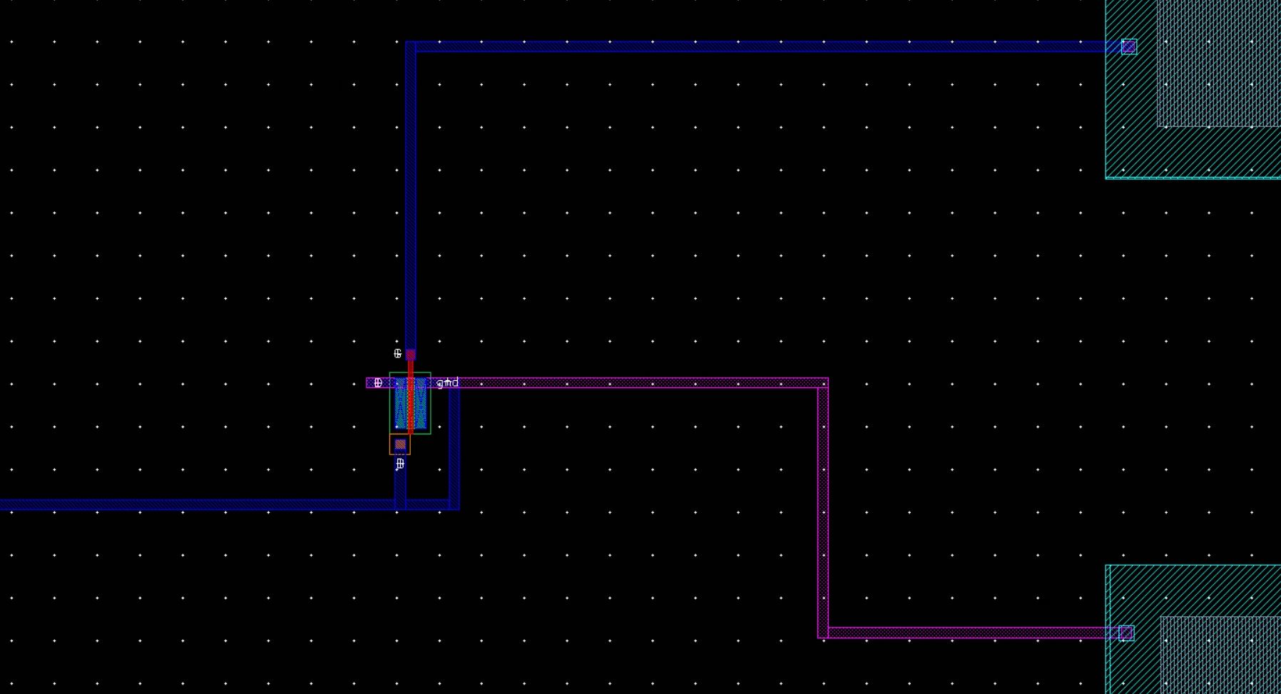
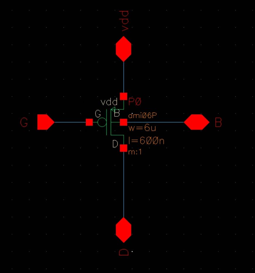
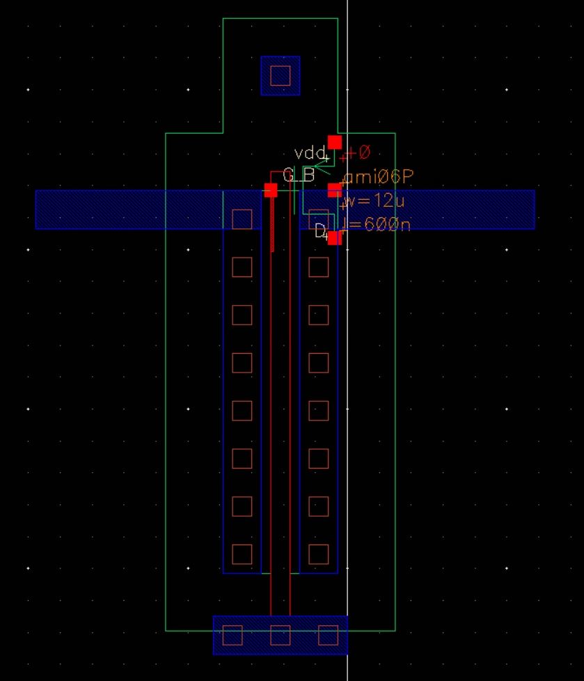
Chip Layout (zoomed into PMOS):
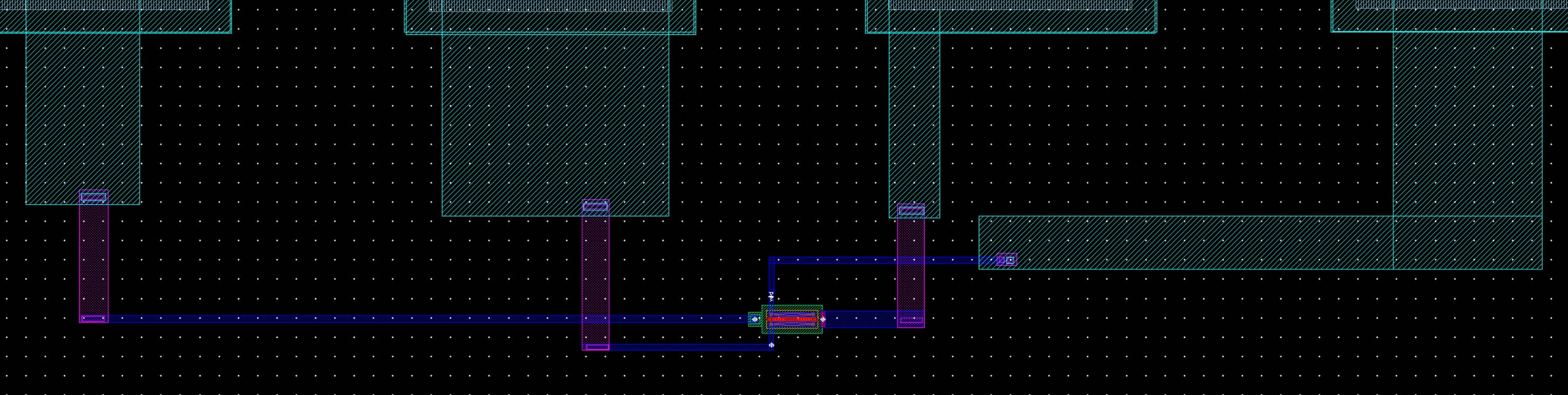
Chip Layout (zoomed into NAND):
Chip Layout (zoomed into NOR):
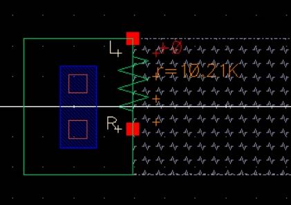
Chip Layout (zoomed into voltage divider):
Chip Layout (zoomed into inverter):
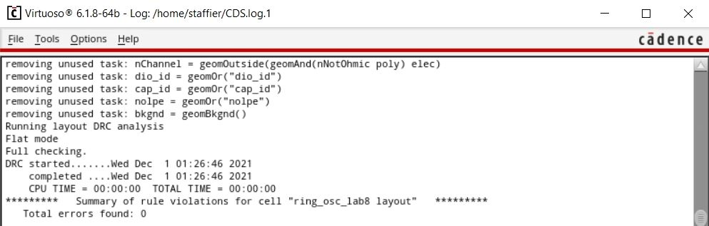
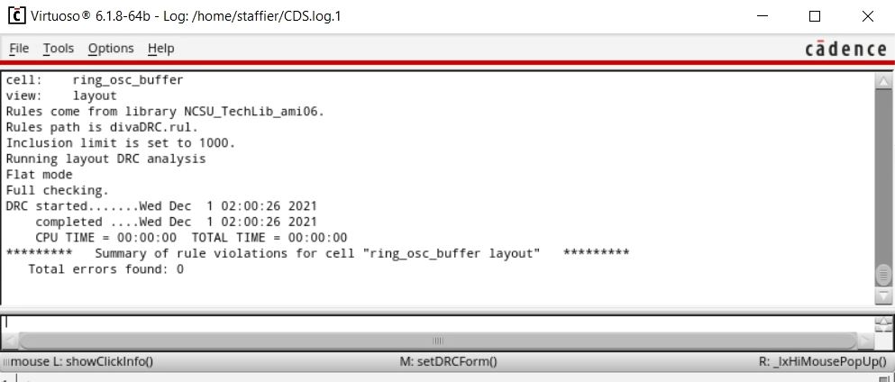
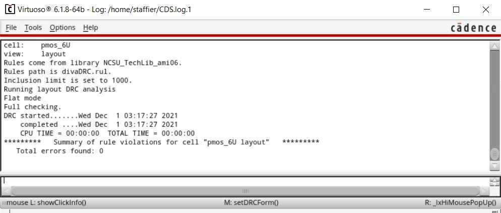
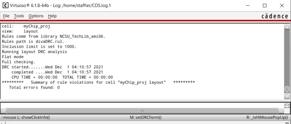
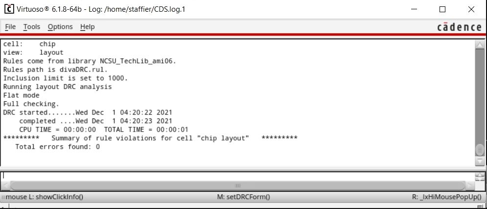
Chip DRC Clean:
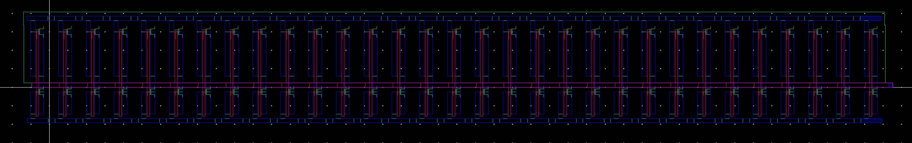
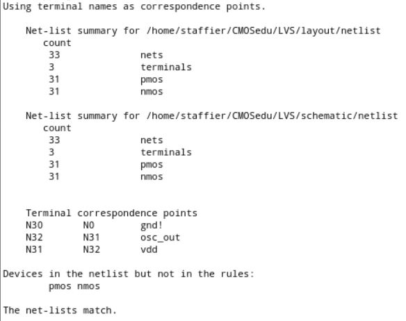
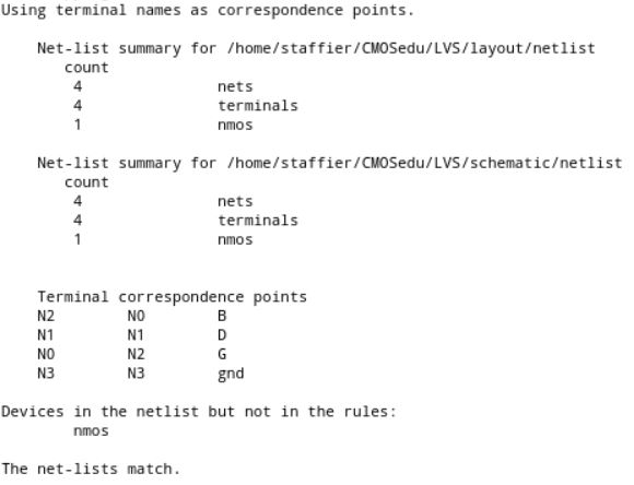
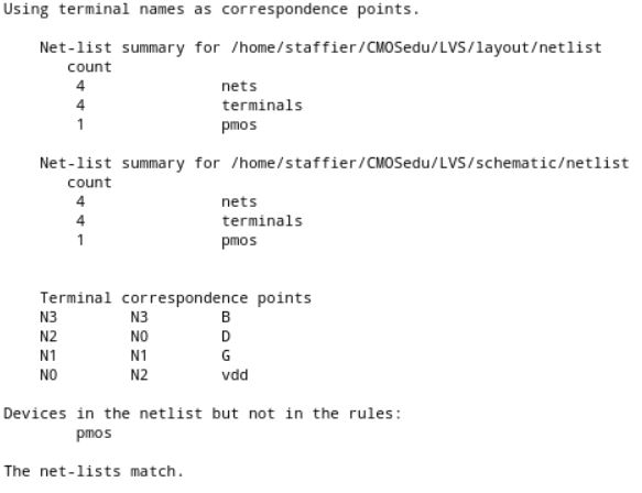
Chip Extracted:
Backup
The online backup of our completed files can be downloaded here.