Final Project - ECE 421L
Brandon StaffieriNOTE: Throughout various points in the project, I will use both 12u/6u and 1.5u/1.5u inverters. The 1.5u/1.5u inverter is almost identical in design to the 12u/6u, with the only change being the obvious size difference of the PMOS and NMOS devices. As I have already documented my inverter design in my Lab 5 Report, I will not be including those images or descriptions here, focusing only on newly drafted designs for this project.
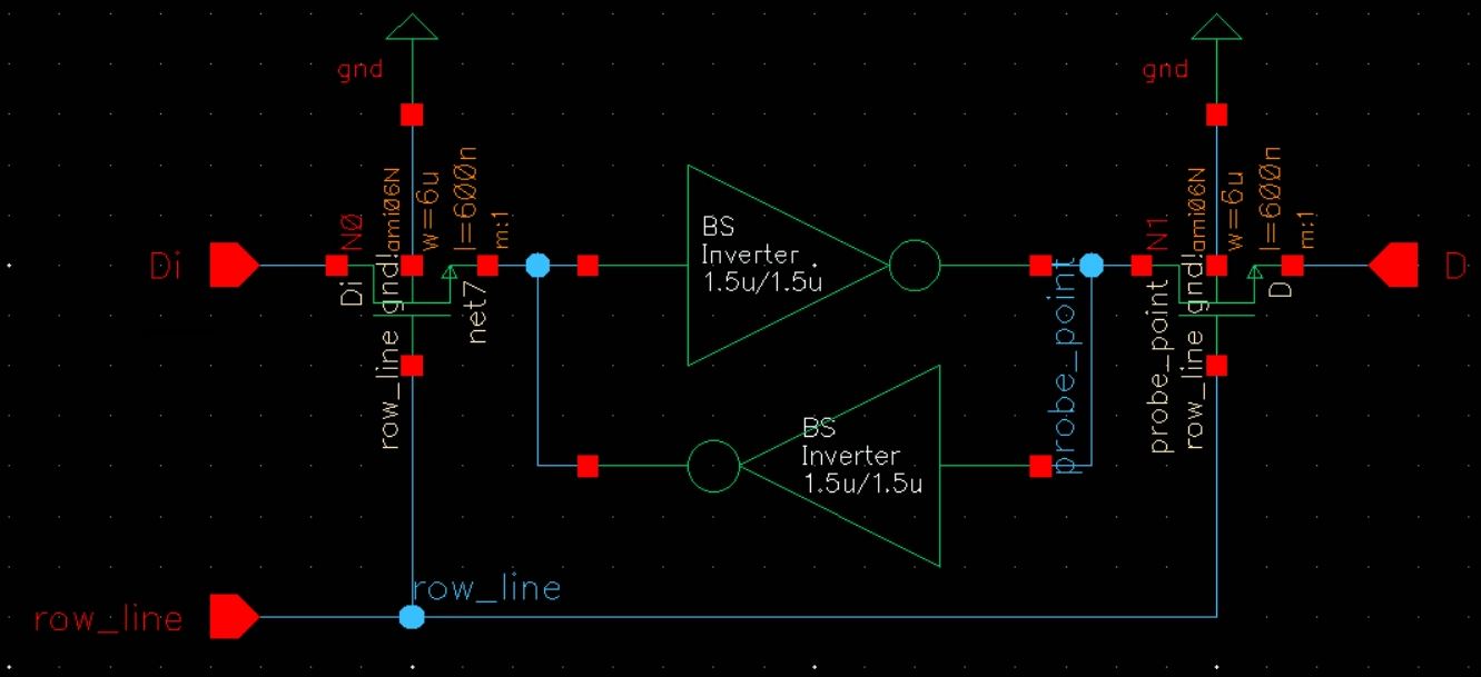
1-bit SRAM Schematic:
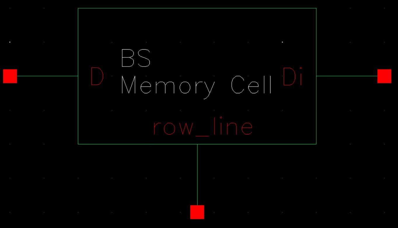
1-bit SRAM Symbol:
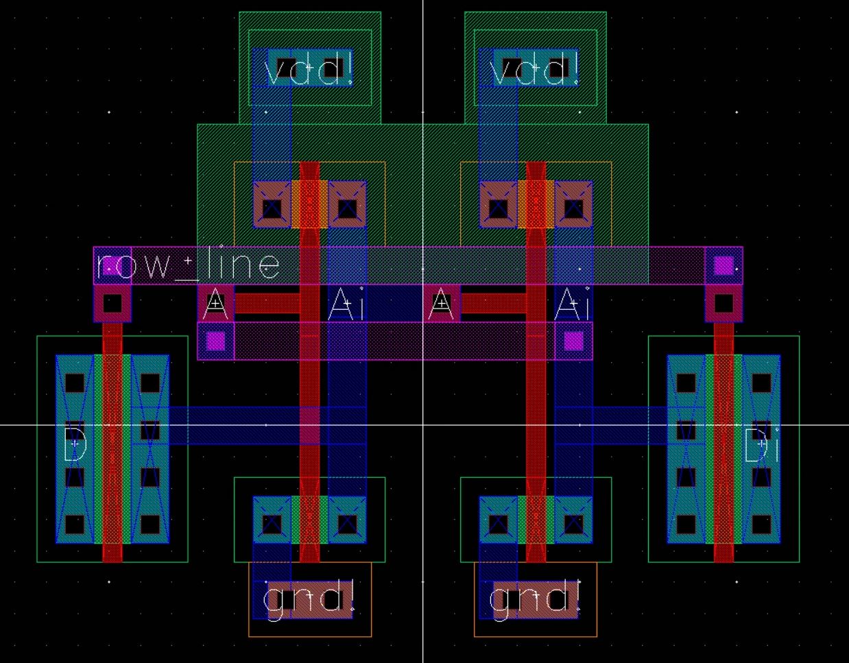
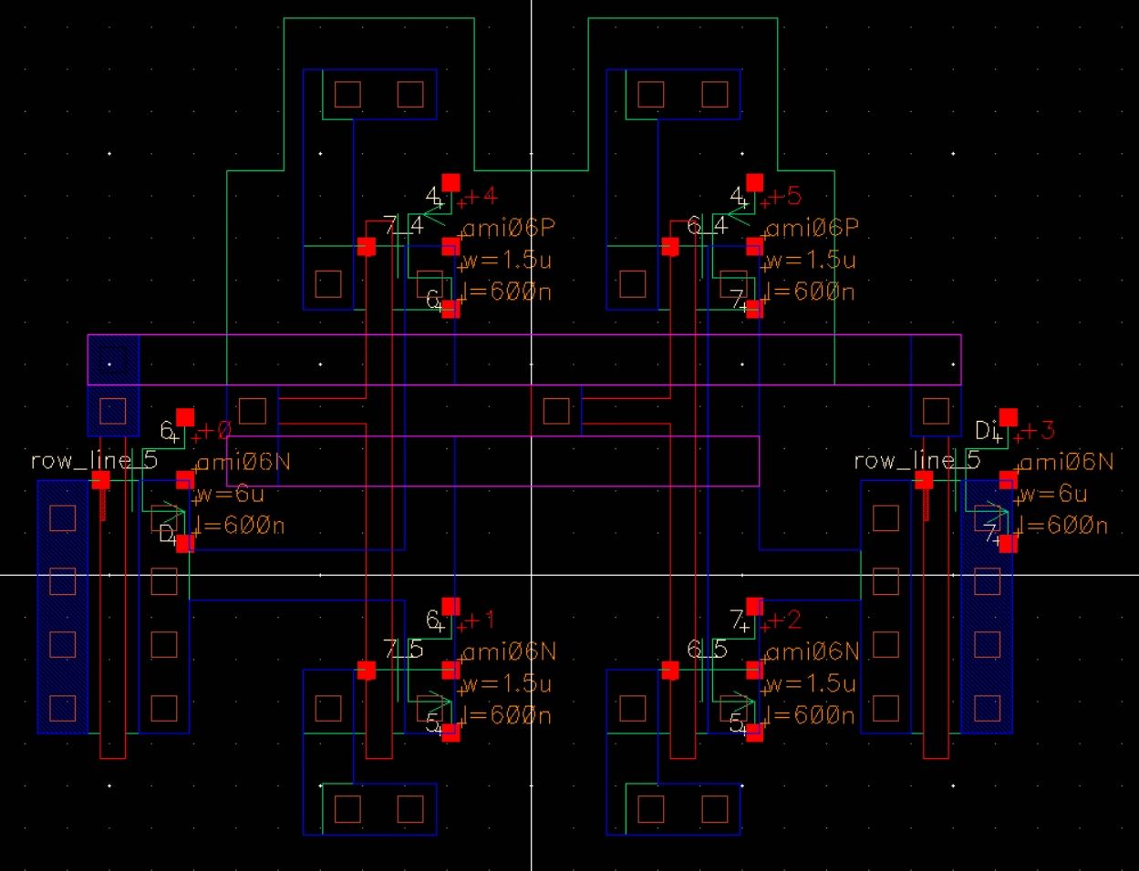
1-bit SRAM Layout:
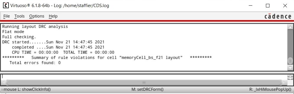
1-bit SRAM DRC Clean:
1-bit SRAM Extracted:
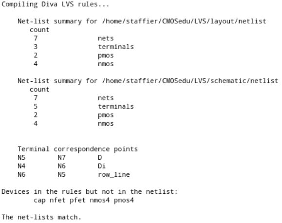
1-bit SRAM LVS Clean:
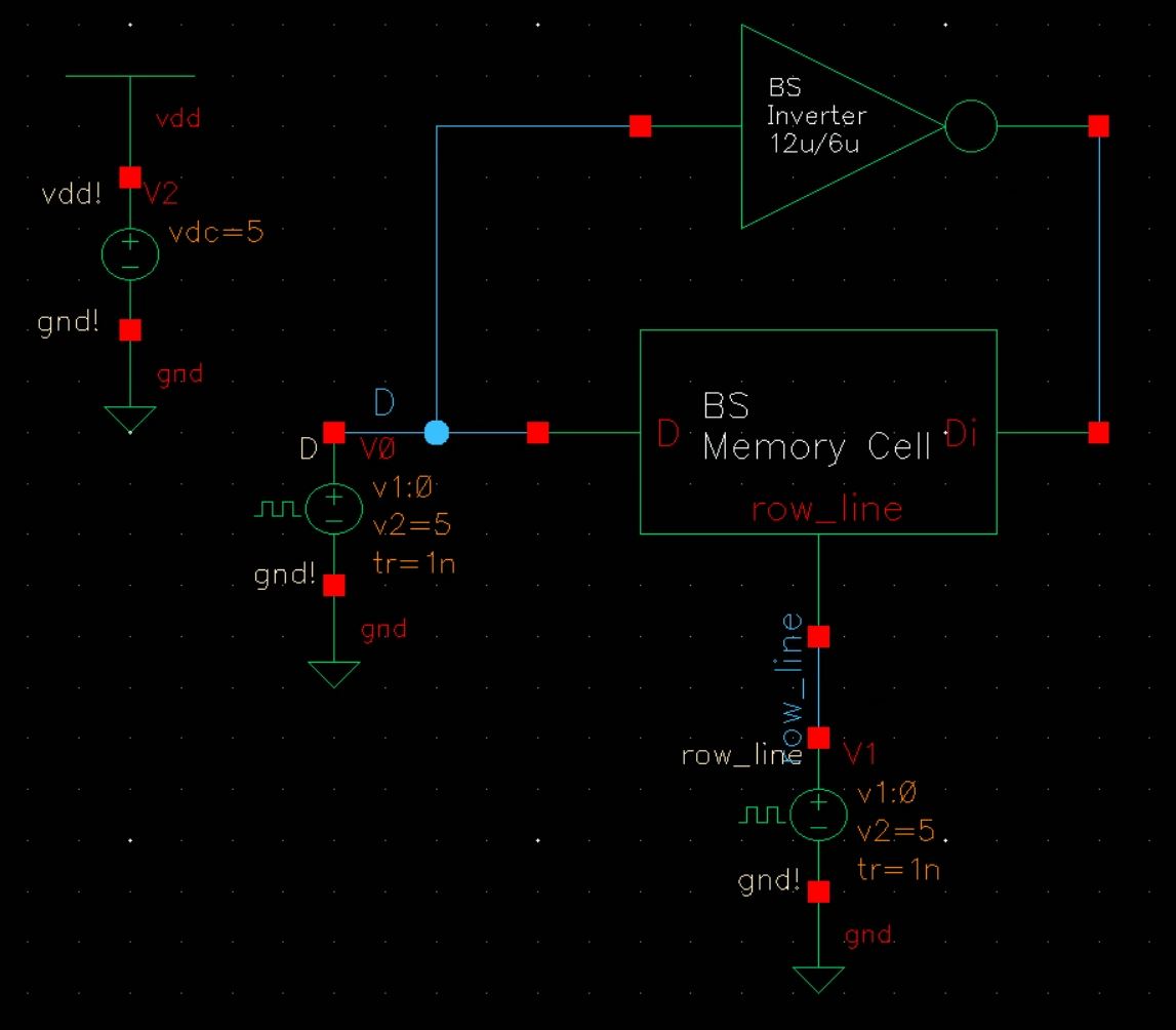
1-bit SRAM Simulation Schematic:
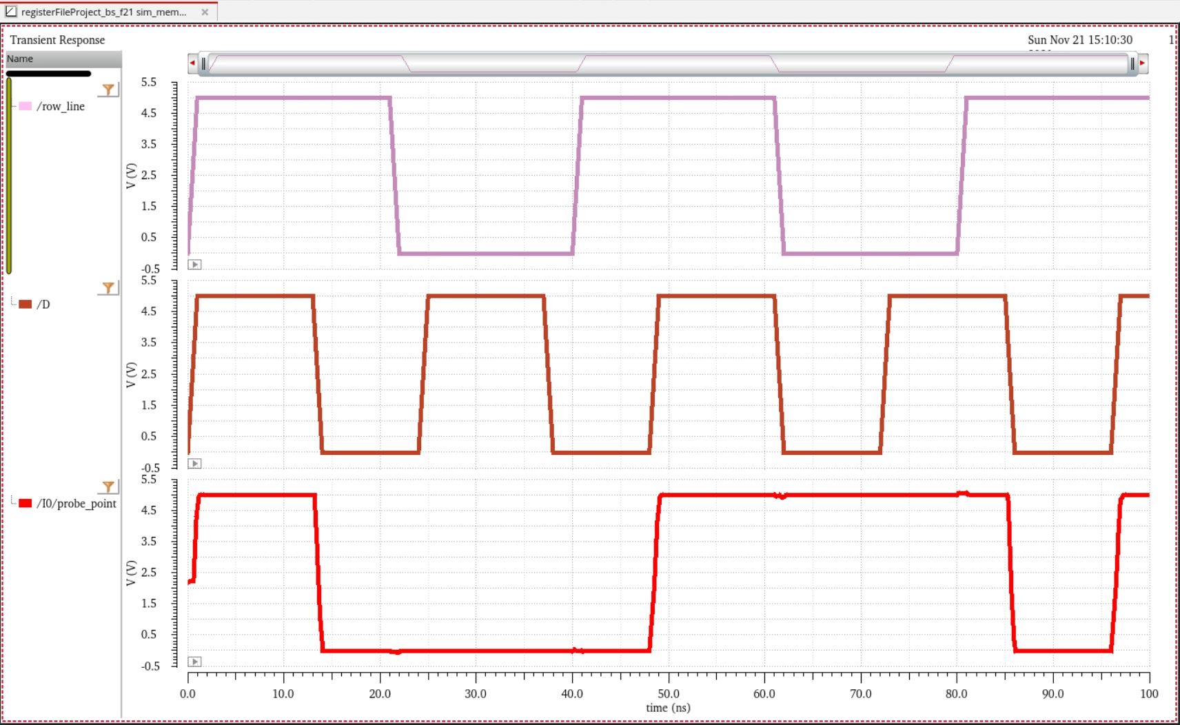
1-bit SRAM Simulation Results:
8-bit SRAM Schematic:
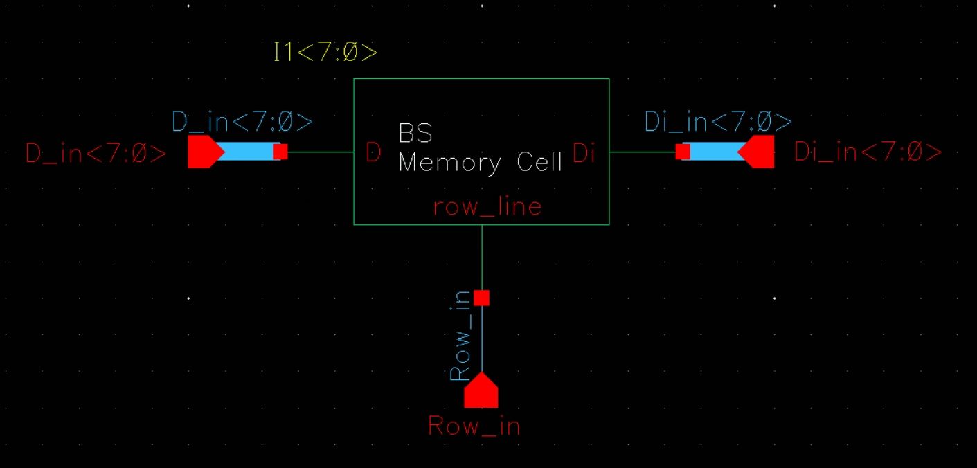
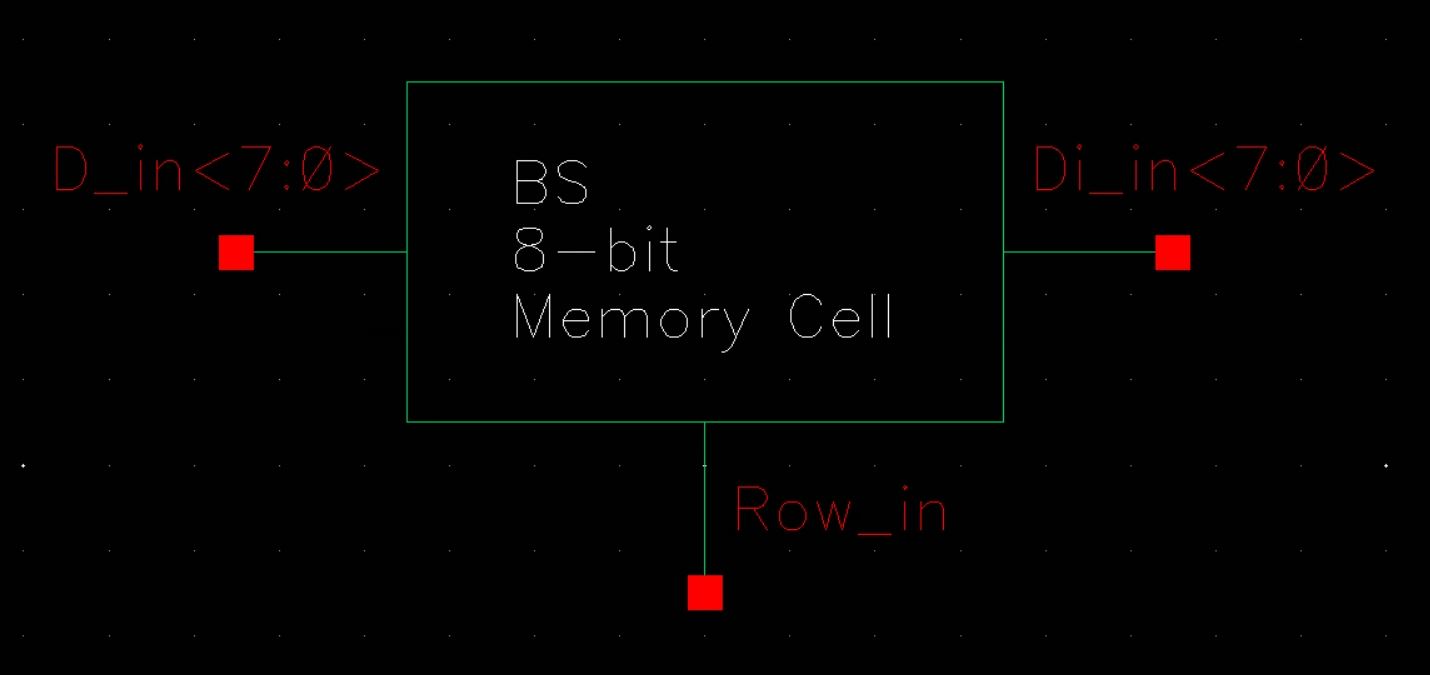
8-bit SRAM Symbol:
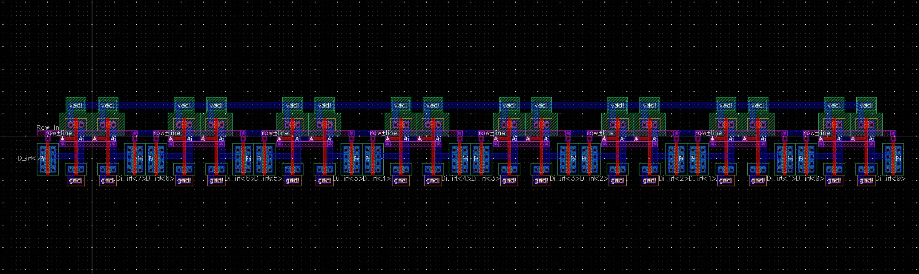
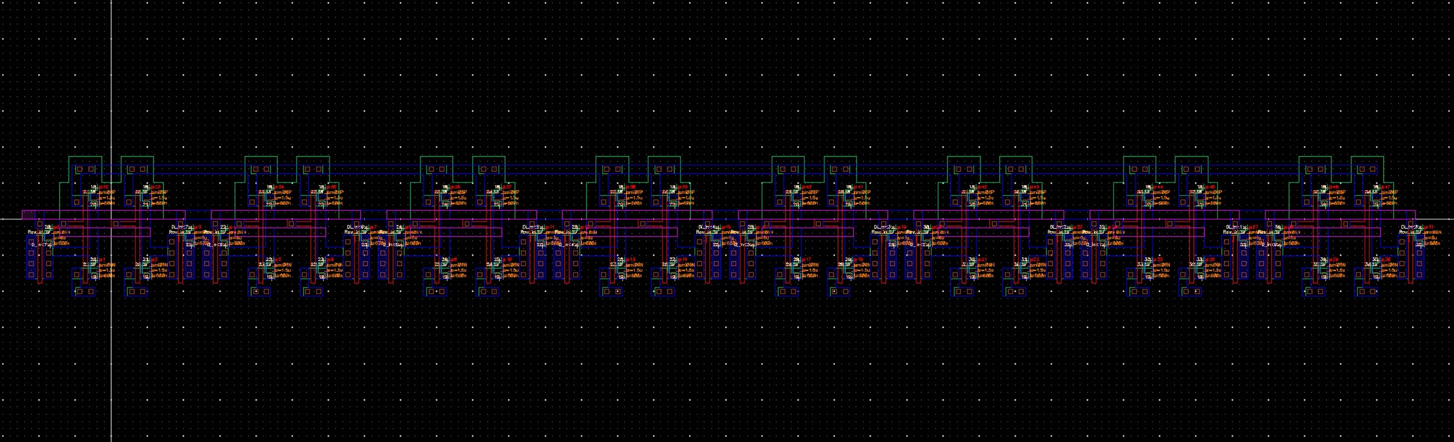
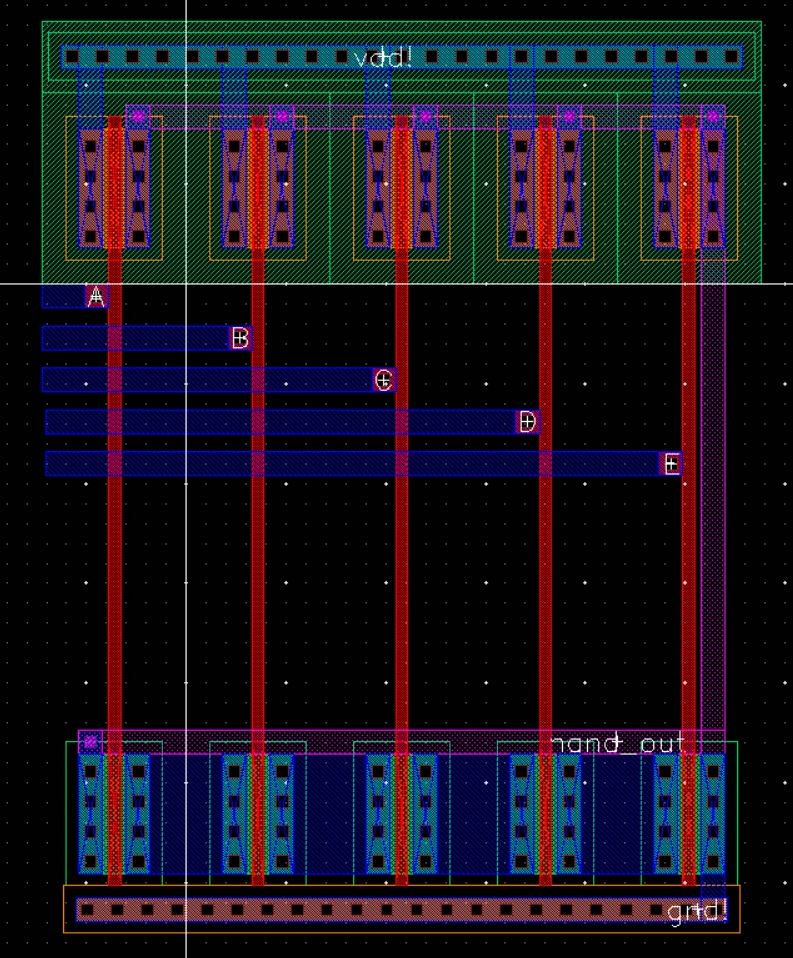
8-bit SRAM Layout:
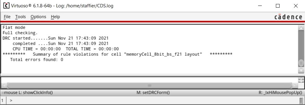
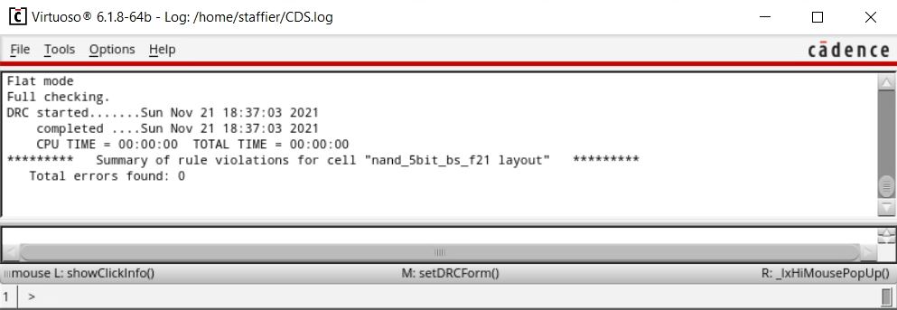
8-bit SRAM DRC Clean:
8-bit SRAM Extracted:
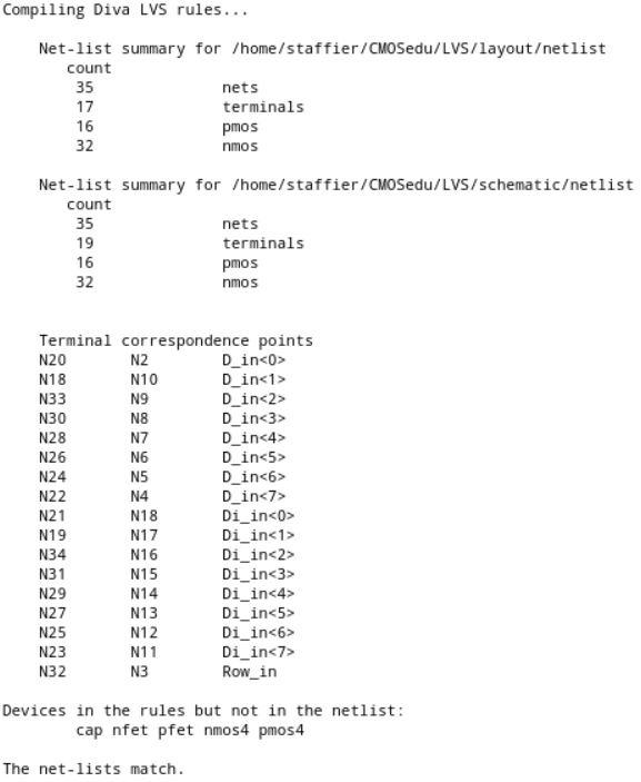
8-bit SRAM LVS Clean:
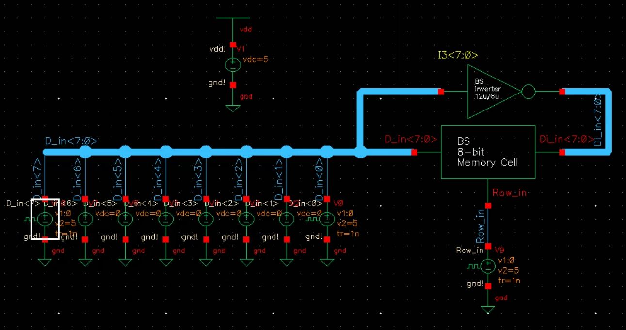
8-bit SRAM Simulation Schematic:
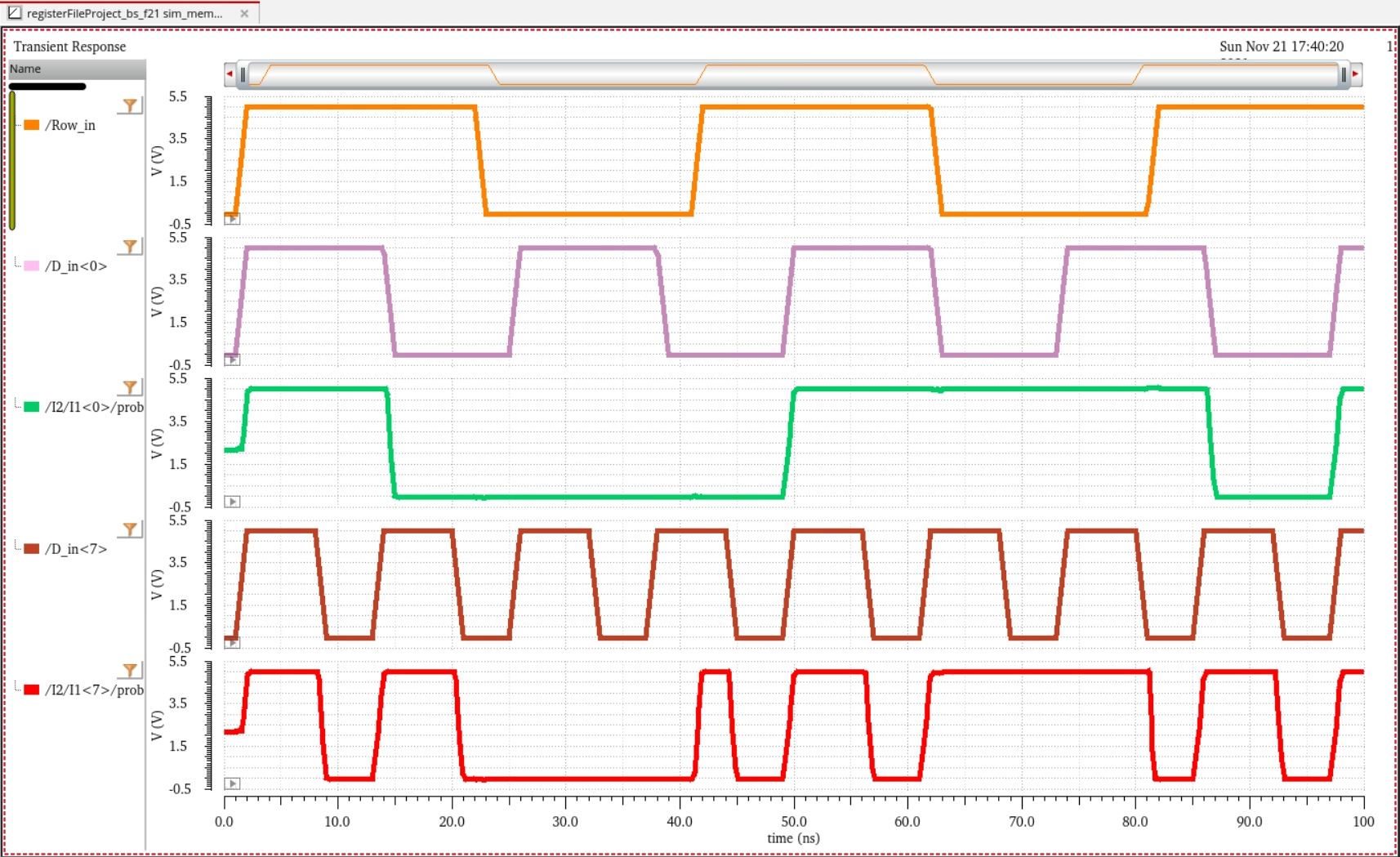
8-bit SRAM Simulation Results:
As
can be observed in the above simulation results, the 8-bit SRAM word is
functioning as intended. The behavior of the instantiated 1-bit SRAM
cells do not change from the previous simulation. When the row line is
high, each of the 8 bits of D<7:0> are stored within their
respective 1-bit SRAM cells (in this example, I grounded every bit
except for D<7> and D<0> which are hooked up to pulse
sources, which is why those are the only ones that I observed and
recorded in the ADE transient simulation). And, when the row line is
low, the D<7:0> values are no longer being written, and the SRAM
cells merely retain the most recently provided data.
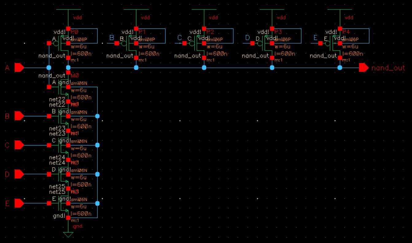
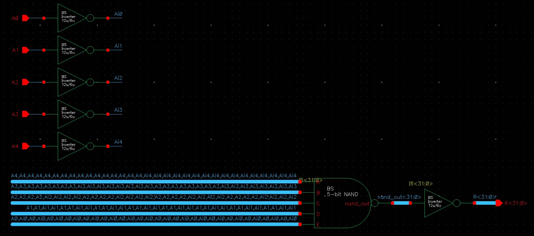
5-bit NAND Simulation Schematic:
5-bit NAND Simulation Results:
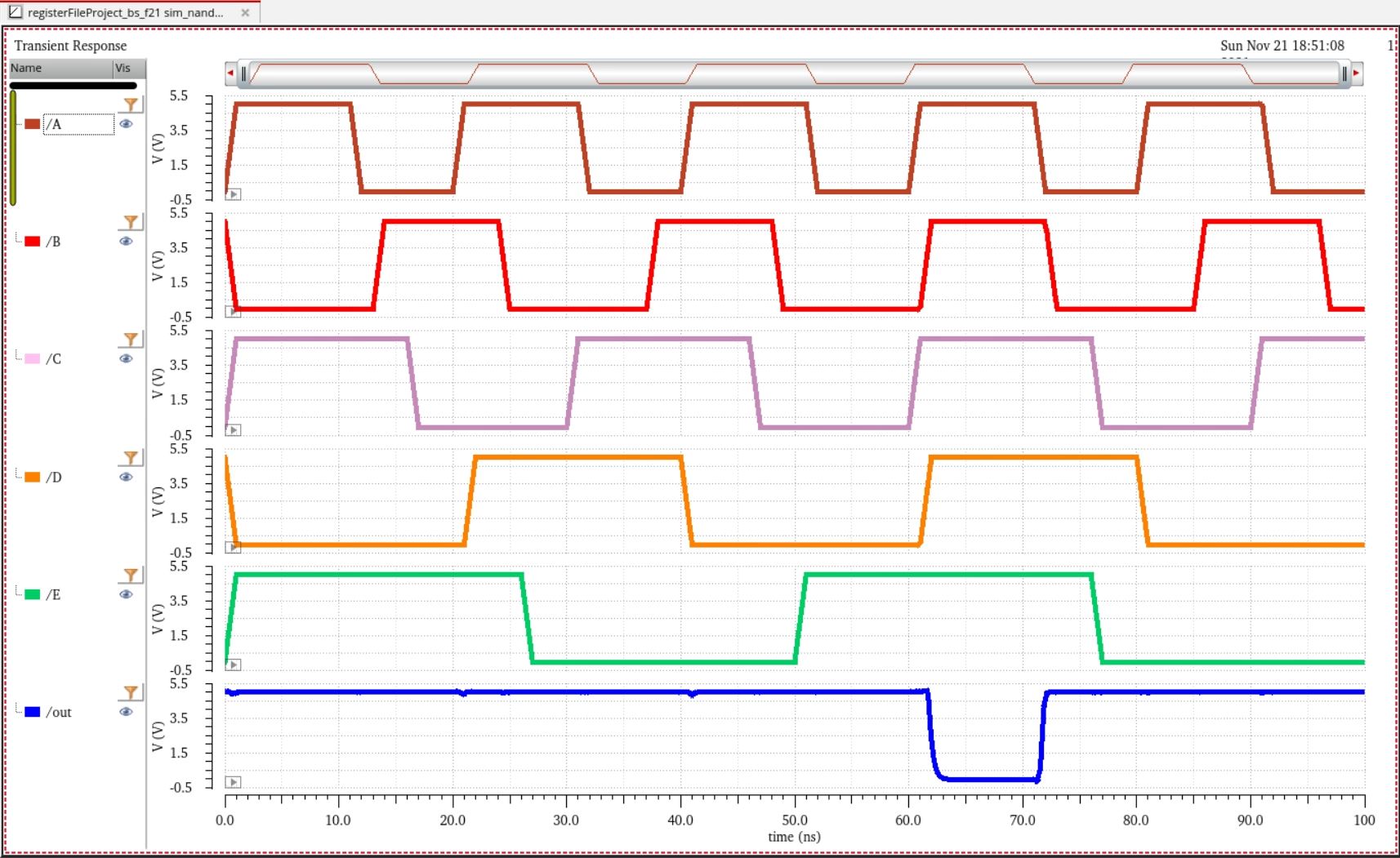
As can be observed in the above simulation results, the 5-bit NAND is functioning as intended. In fulfillment of a 5-bit NAND truth table, the only set of values that result in an output of 0 is when all of the inputs are high.
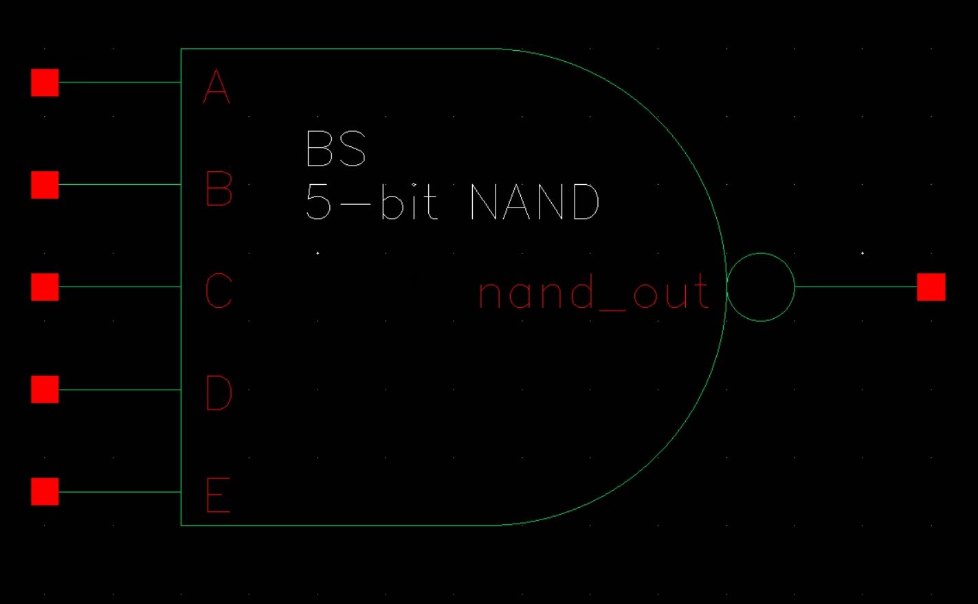
Next, we will use this 5-bit NAND in order to create our row decoder. As explained earlier, the row decoder will instantiate 32 of these NANDs to account for every combination of inputs. Each NAND will have an inverter placed after it to change its operation to be identical to that of an AND-gate; thus, each unqiue AND-gate will only be set high by one specific combination of inputs, which will enable its respective row line.
Row Decoder Schematic:
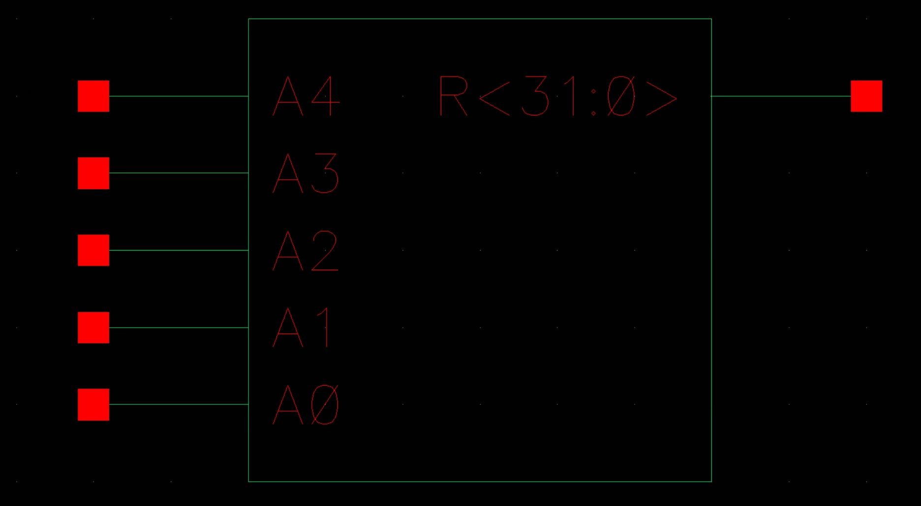
Row Decoder Symbol:
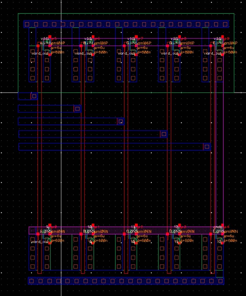
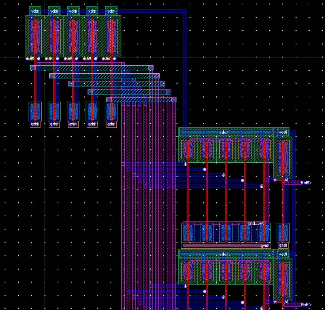
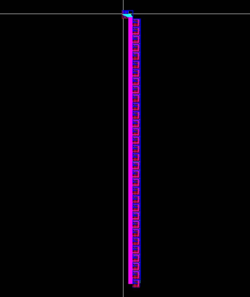
Row Row Decoder Layout:
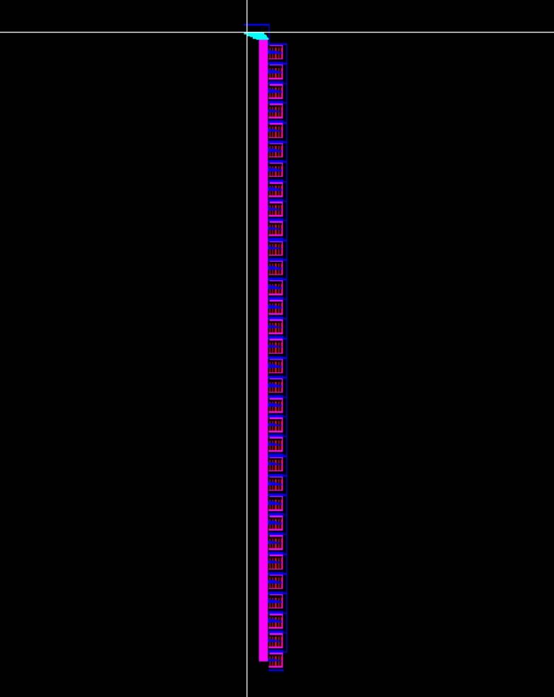
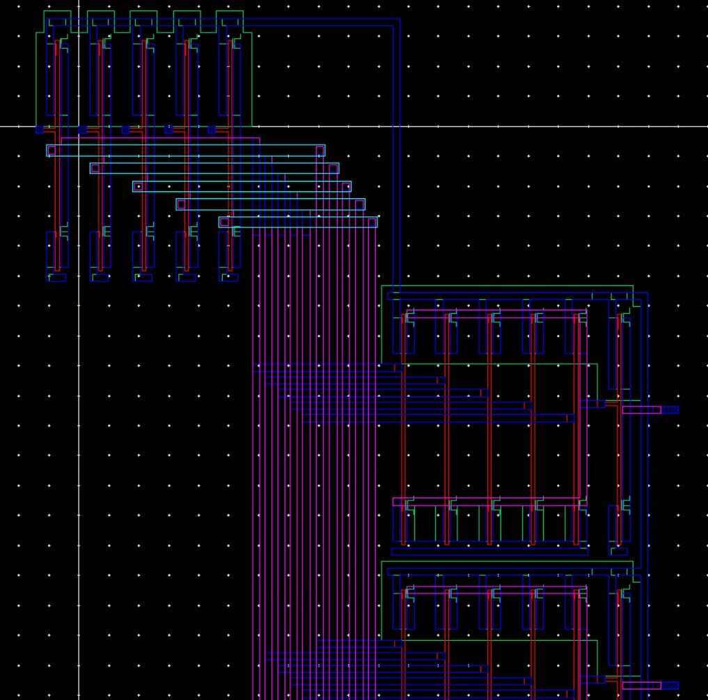
Row Decoder Layout (Zoomed):
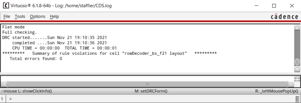
Row Decoder DRC Clean:
Row Decoder Extracted:
Row Decoder Extracted (Zoomed):
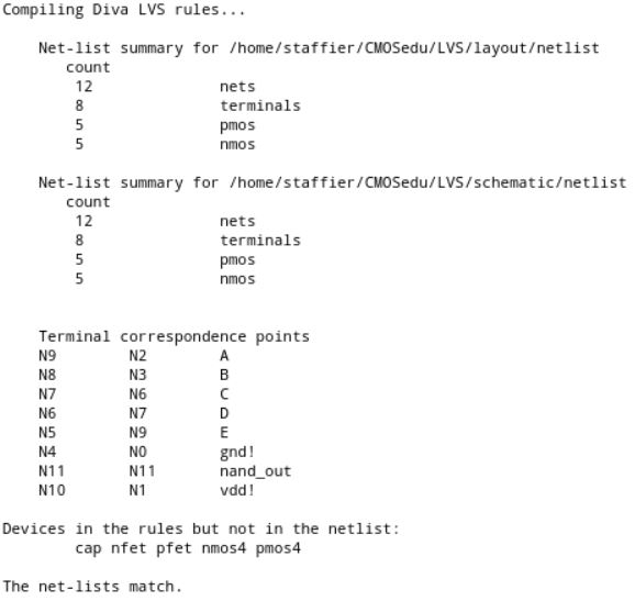
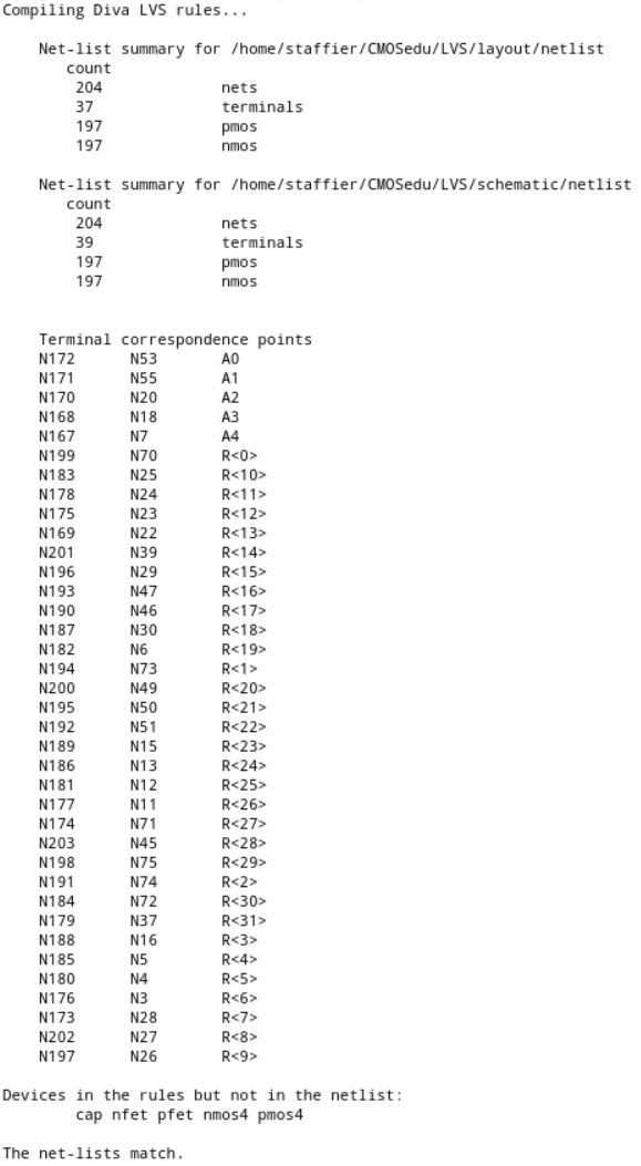
Row Decoder LVS Clean:
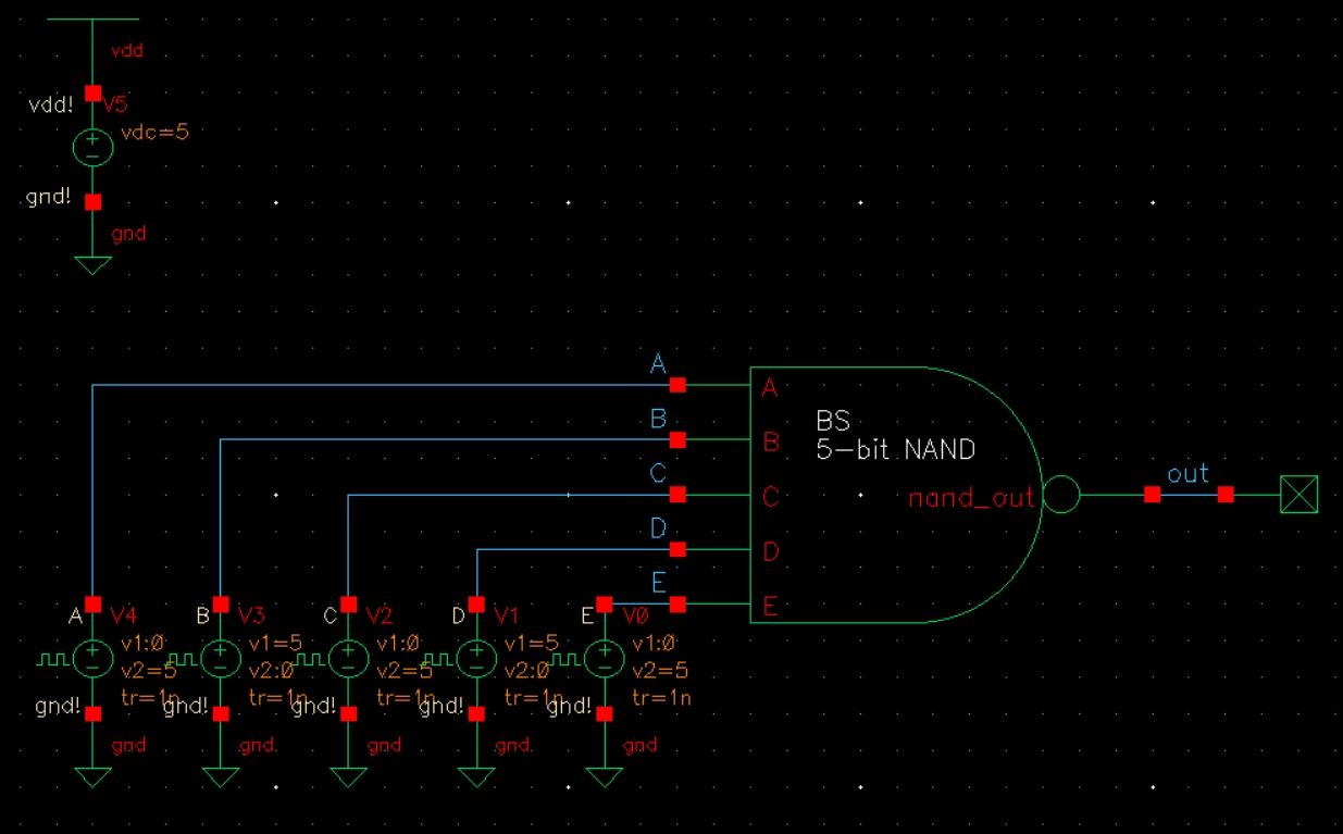
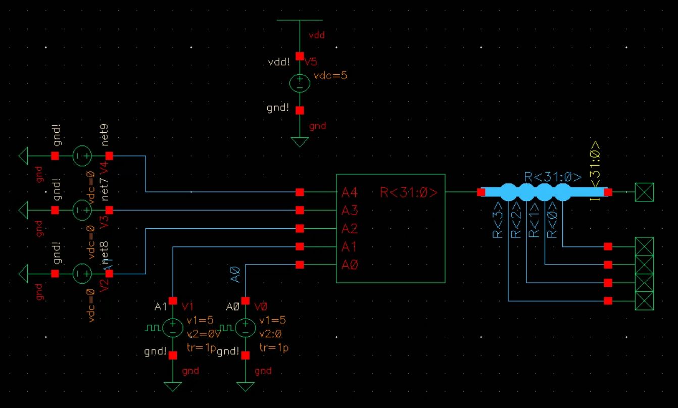
Row Decoder Simulation Schematic:
Row Decoder Simulation Results:
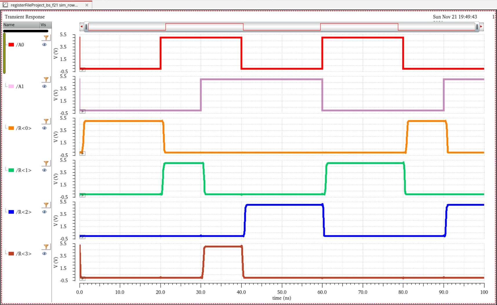
As can be observed in the above simulation results, the row decoder is functioning as intended. The 5-bit input that serves as our address can be directly correlated to which row is enabled at any given time. For this demonstration, I pulsed only the lower 2 bits and grounded the rest. As would be expected if one converted the binary input to its decimal value, the input 00 enables row 0, 01 enables row 1, 10 enables row 2, and 11 enables row 3. This behavior will continue all the way up until row 31 (which is the 32nd and final row).
Lastly, the only thing left is to put everything together and draft the design for the register file. As all the components have now been created, this last step is a relatively straight forward task. The register file simply takes an address into the row decoder to determine which 8-bit memory cell needs to be accessed, and either writes the D_in<7:0> values into the word cell, or reads the values from the word cell into D_out<7:0> (in theory; however, in this case I will, as instructed by Dr. Baker, only be writing to this cell and manually reading values with a probe to confirm changes to the 8-bit SRAM's stored data, which is done in order to circumvent the previously mentioned design issue at the top of the page).
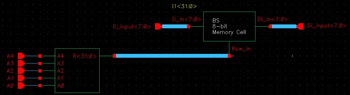
Register File Schematic:
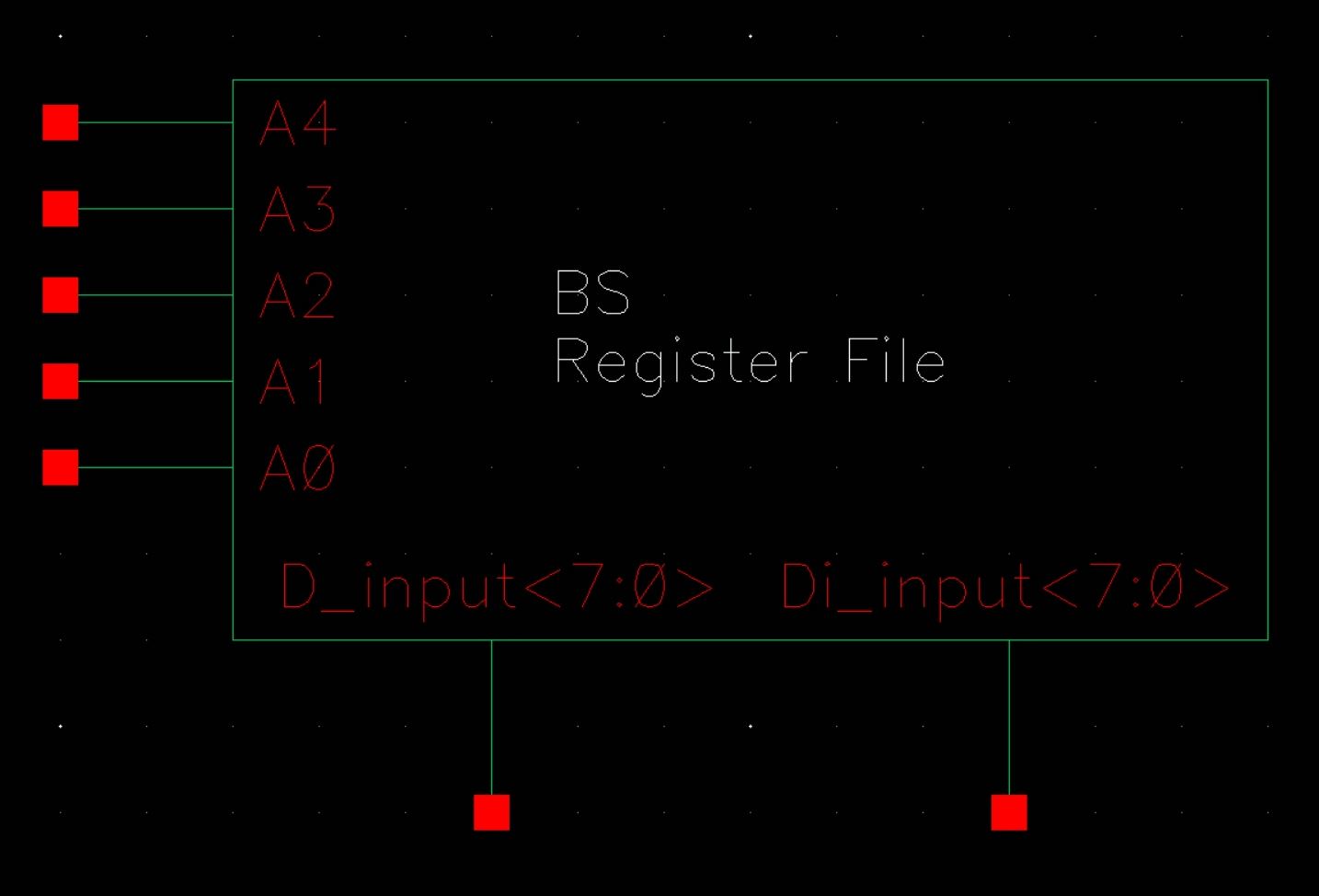
Register File Symbol:
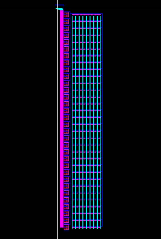
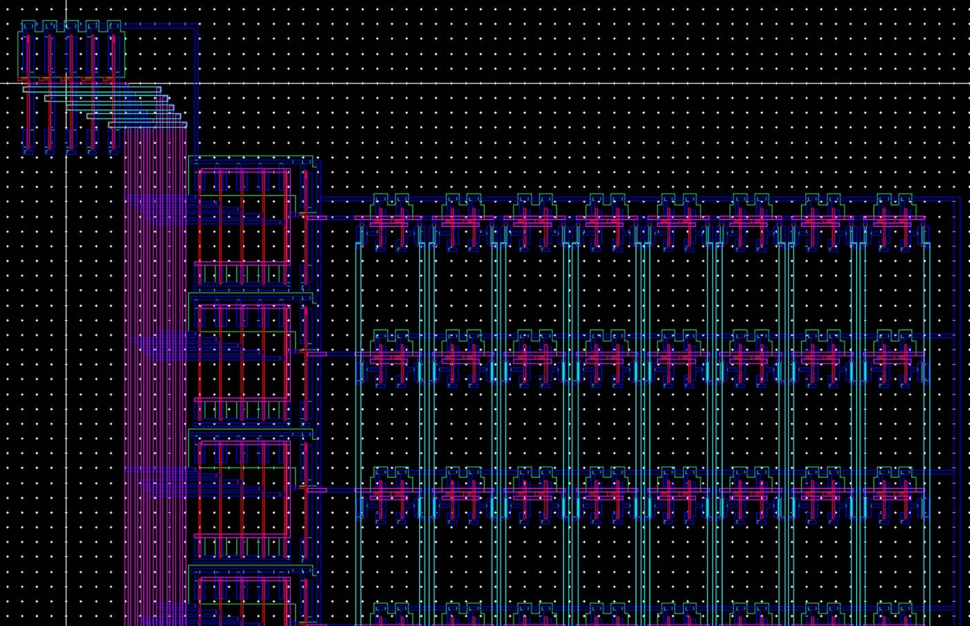
Register File Layout:
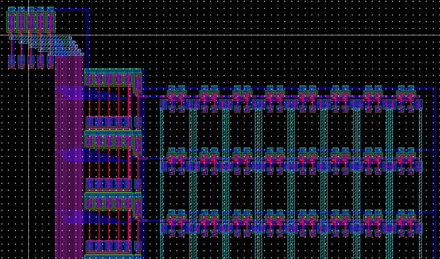
Register File Layout (Zoomed):
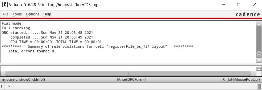
Register File DRC Clean:
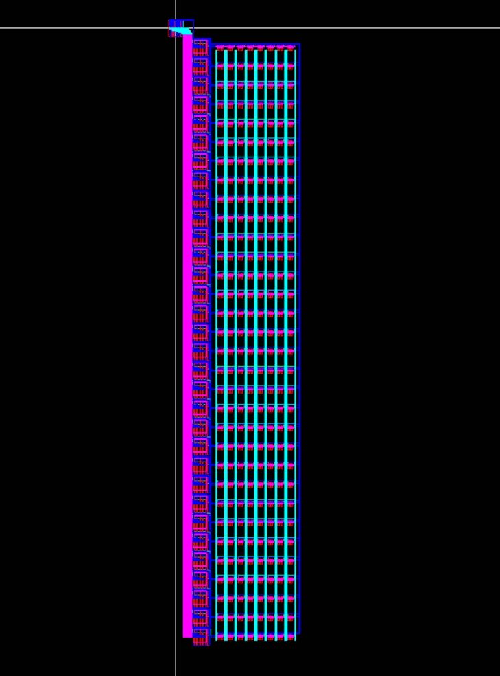
Register File Extracted:
Register File Extracted (Zoomed):
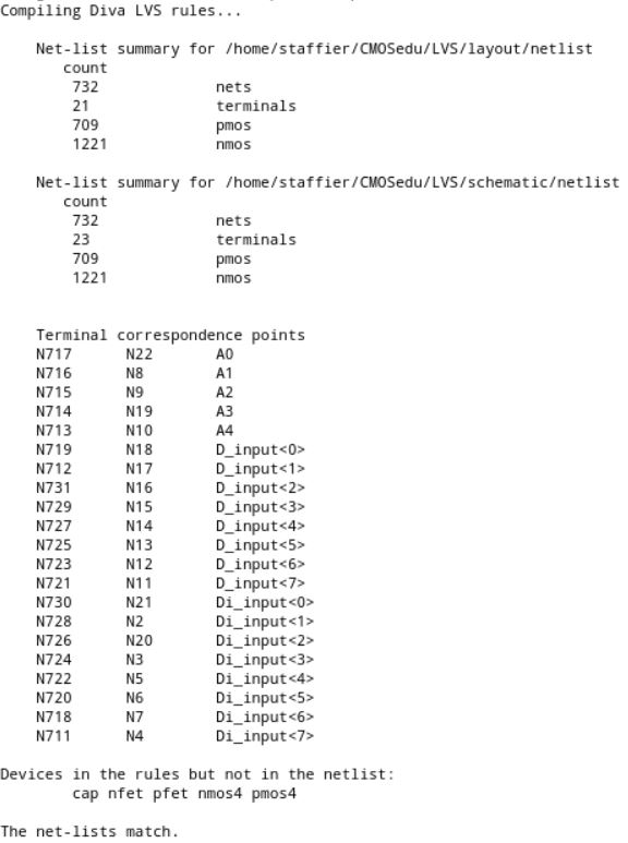
Register File LVS Clean:
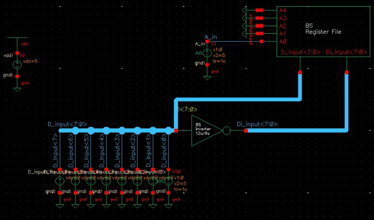
Register File Simulation Schematic:
Register File Simulation Results:
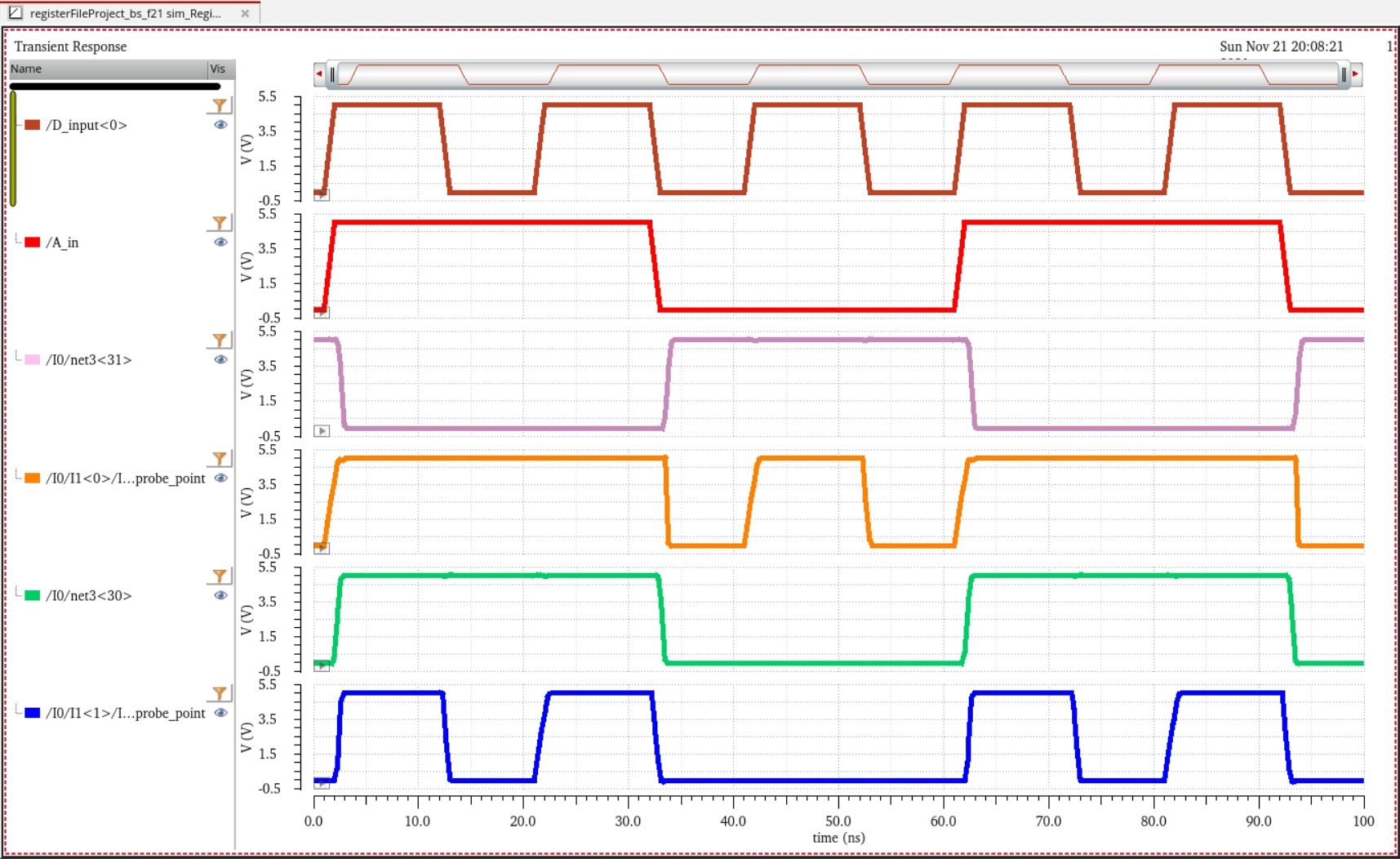
As can be observed in this final simulation, the register file is functioning as intended. The rows used in this example are row 0 and row 1. When the value of the 5-bit address is 1, row 1 is enabled and the probe point shows that the associated least significant bit (LSB) SRAM cell is taking in whatever data that is provided by the D<0> input. When the value of the 5-bit address switches from 1 to 0, the LSB SRAM cell associated with row 1 stops accepting new data and maintains the last known bit. This happens in conjuction with row 0 becoming enabled along with its LSB SRAM cell, and now it is accepting the data provided by the D<0> input instead.
Backup
My online backup of my completed files can be downloaded here.