Lab 7 - ECE 421L
Created and edited by Michael Parker
Email : parkem3@unlv.nevada.edu
Last updated : November 3, 2021
Pre-Lab
- Back-up all of your previous work from the lab and the course.
- Go through tutorial 5 seen here.
Lab Overview
The purpose of this lab is practice the use of buses and arrays in the design of inverters, muxes, and high speed adders.
Lab Procedures
The
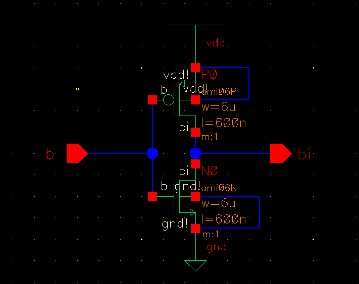
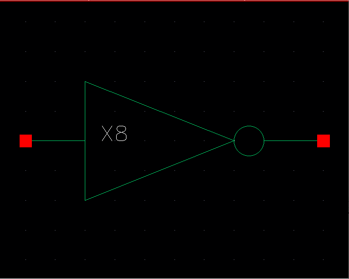
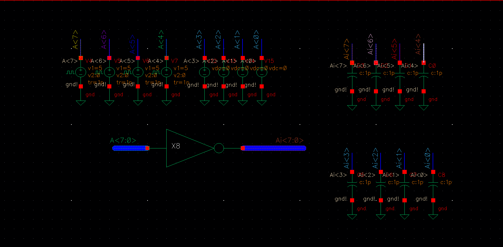
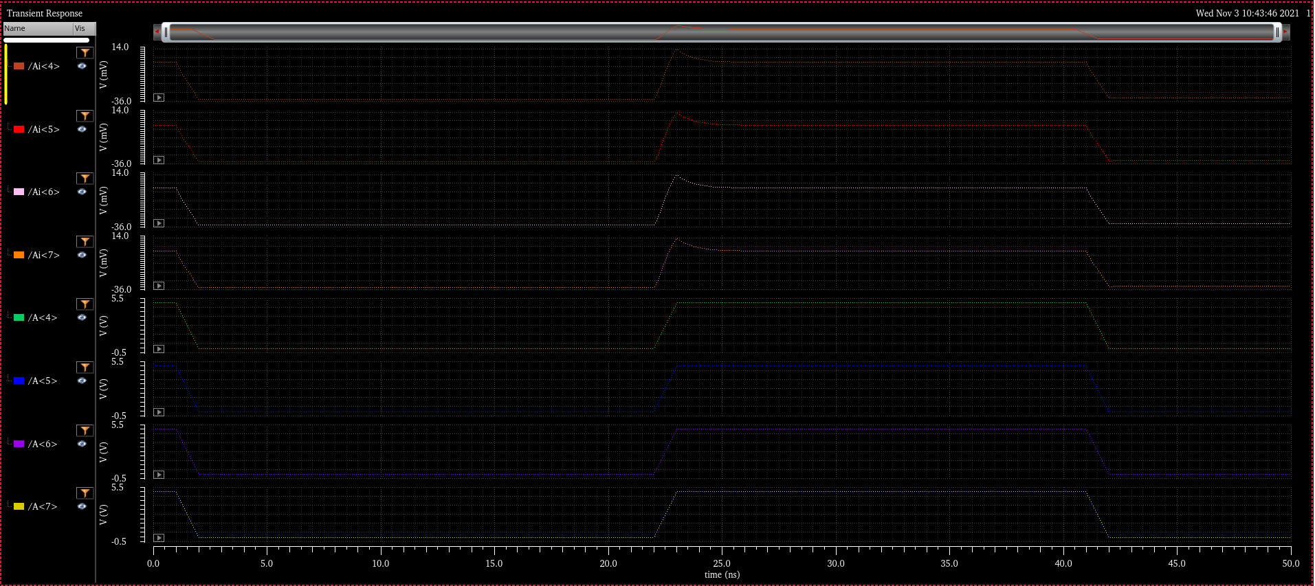
first task for this lab was to create a schematic of an instanced
inverter using a 4 bit bus on the input and the output, creating a
symbol from that inverter and simulating those inverters driving
different capacitive loads.
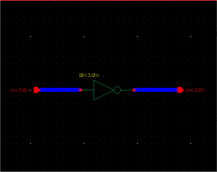
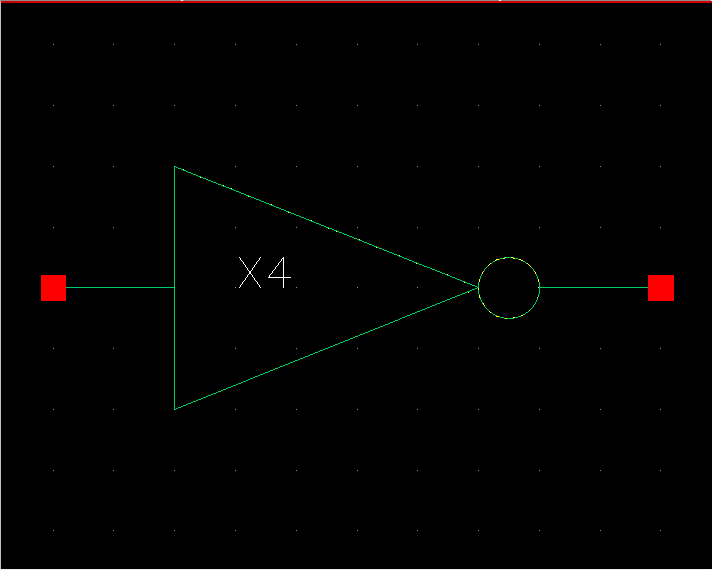
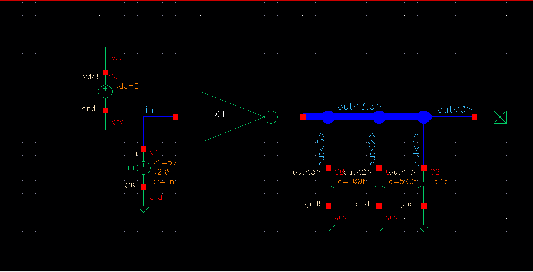
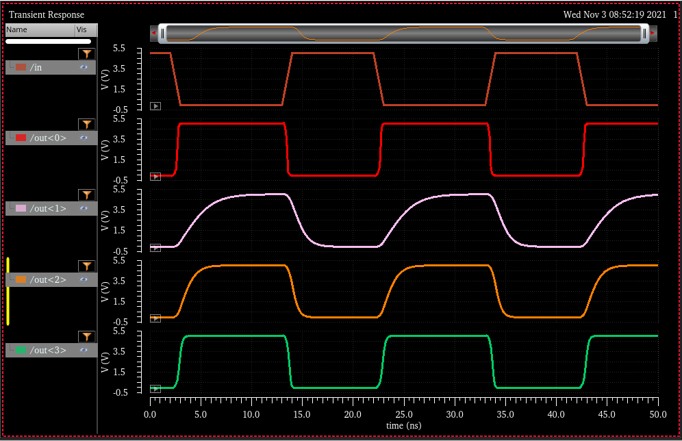

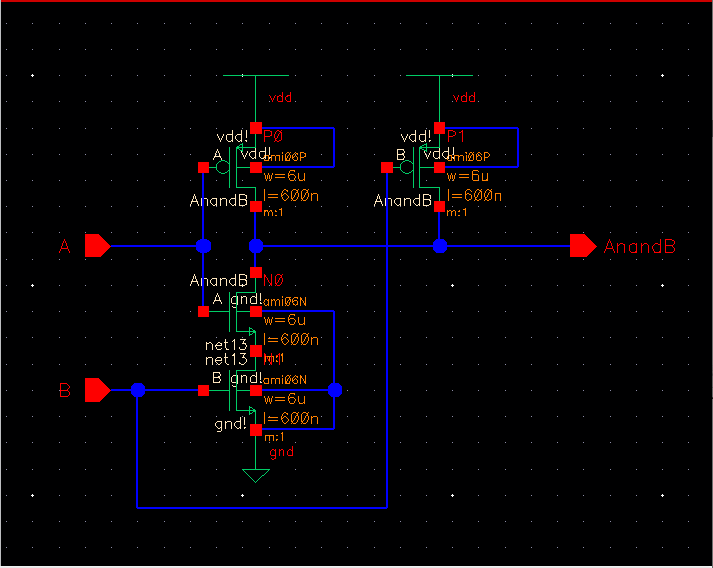
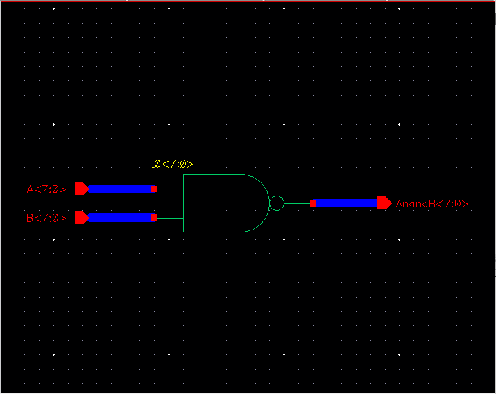
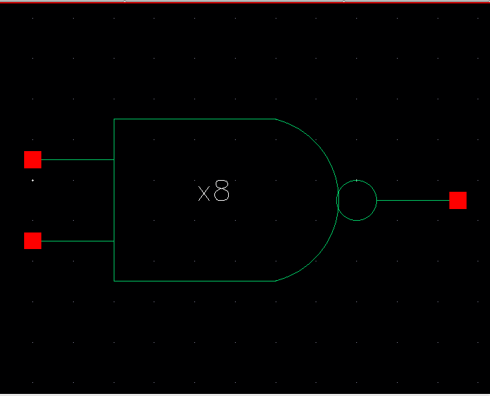
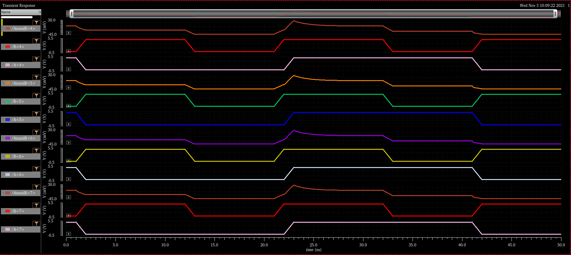
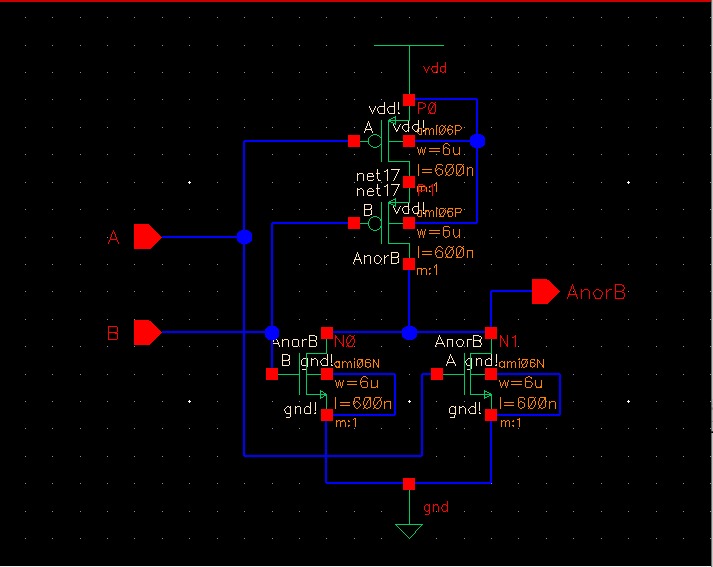
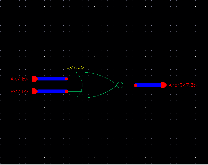
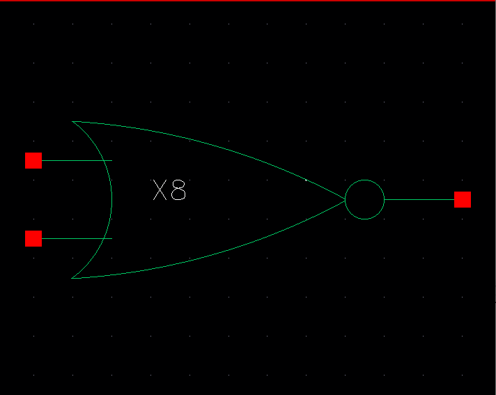
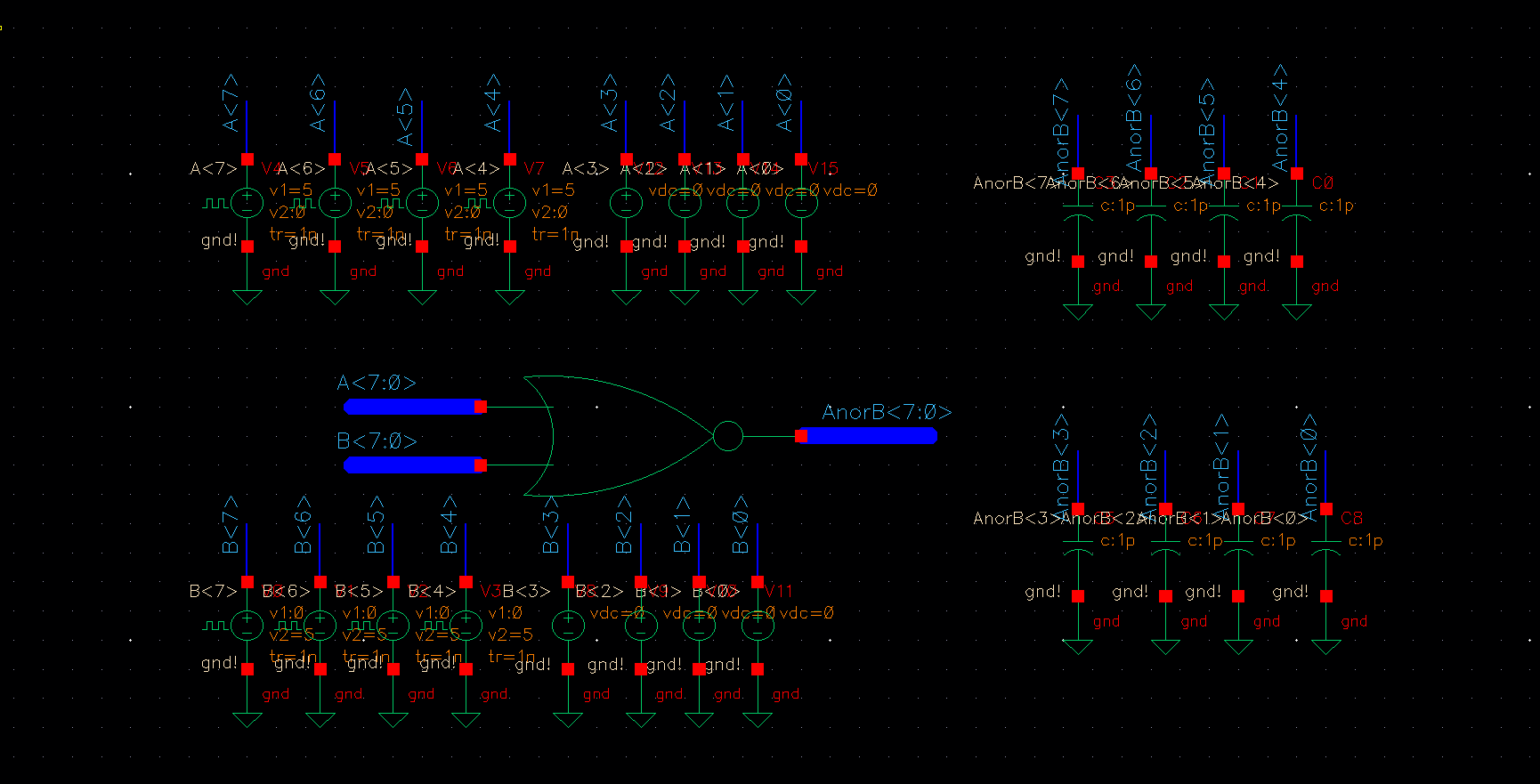
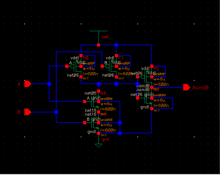
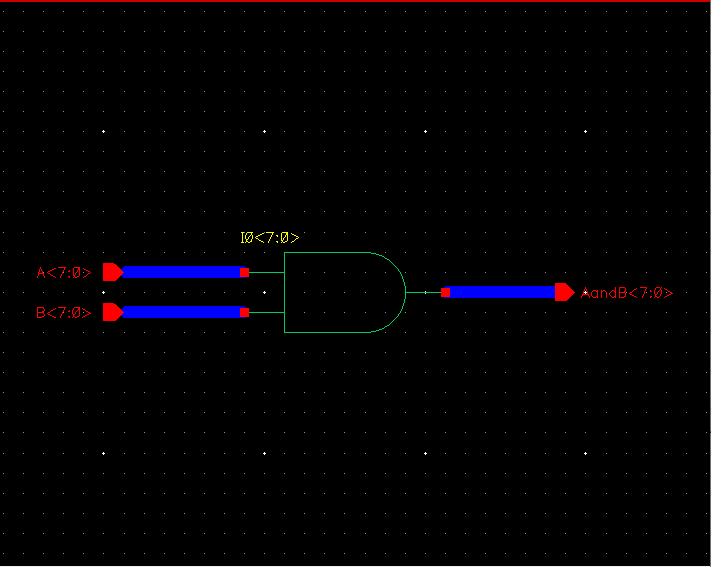
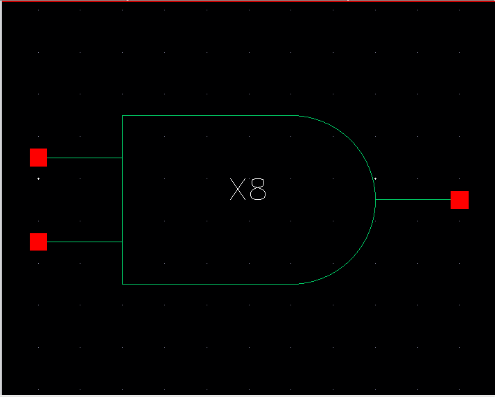
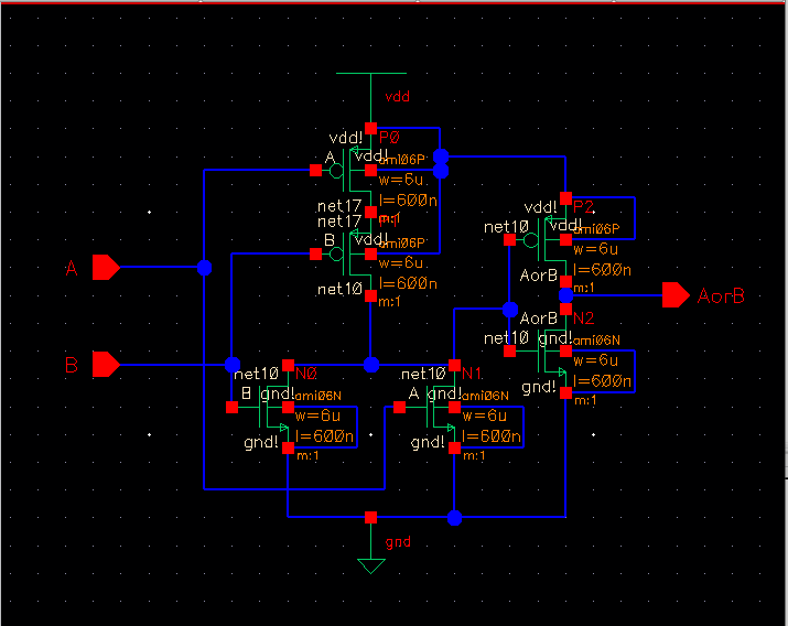
The next task was to create schematics, symbols, and simulate those designs for multiple logic circuits.
NAND

NOR
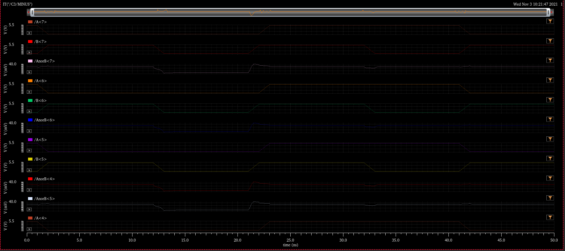
AND
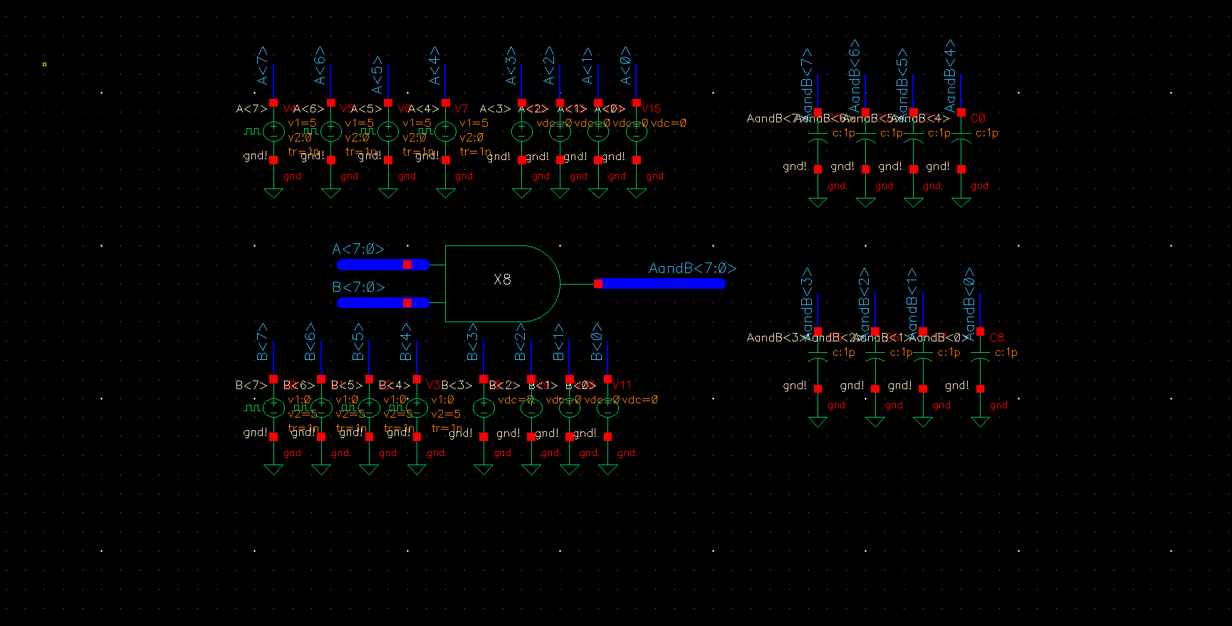
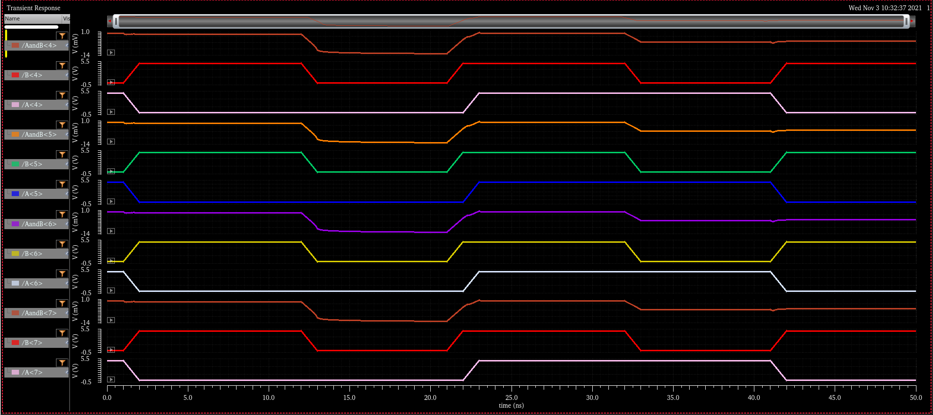
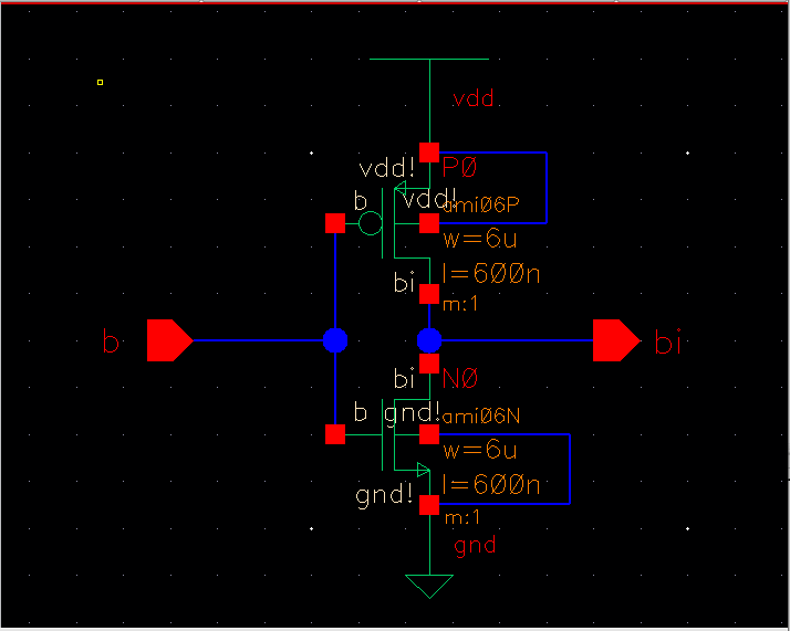
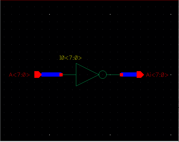
INVERTER
OR
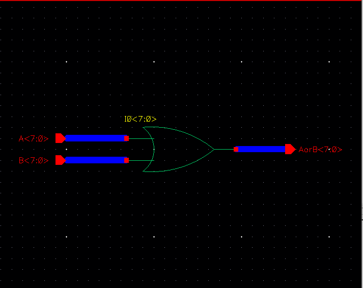
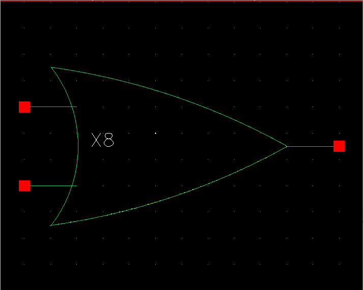
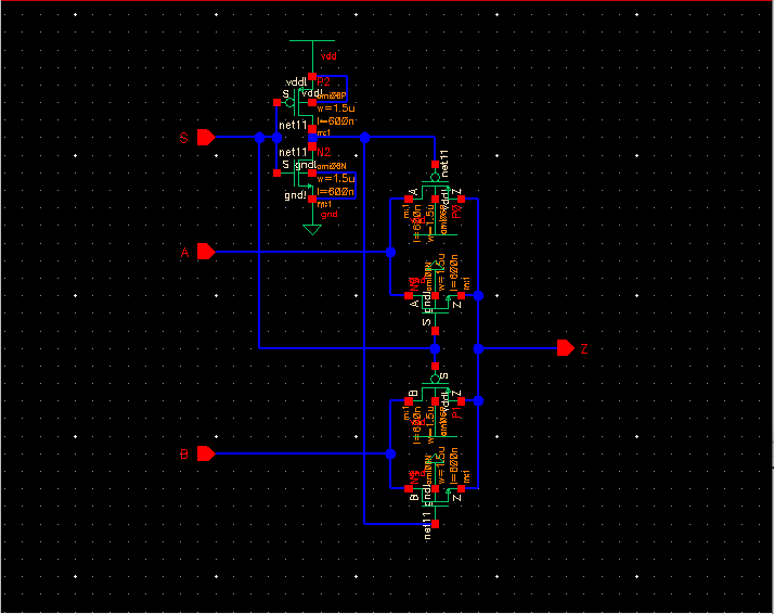
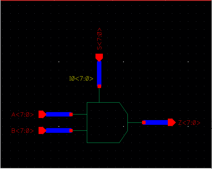
The third task was to create an 8-bit wide 2 to 1 DEMUX/MUX, the symbol and simulating that design.
The
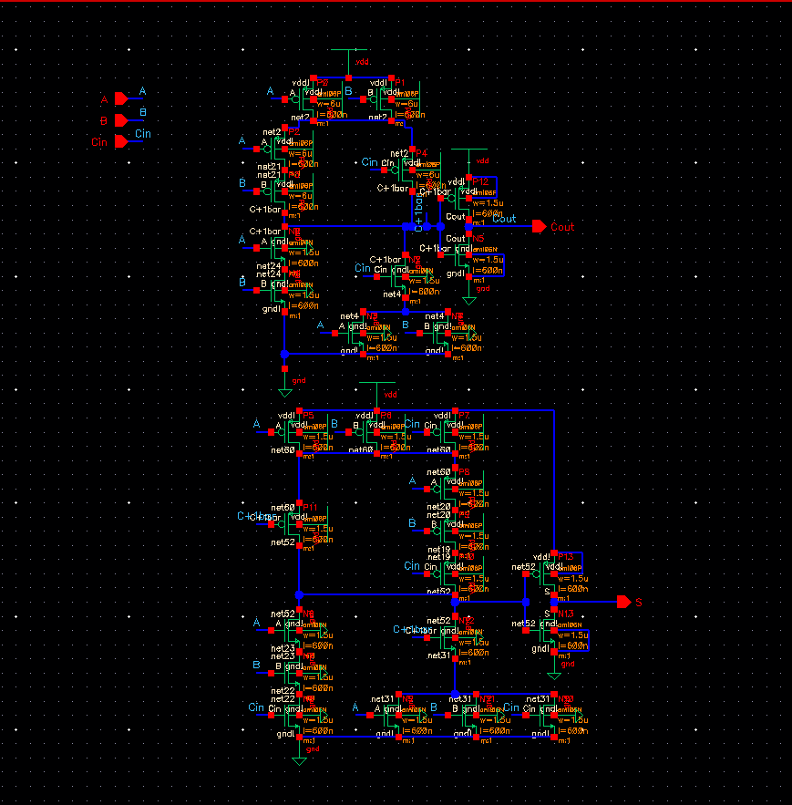
last task was to draft an schematic of the full adder seen in Fig.
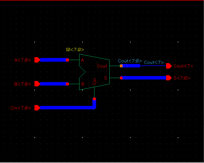
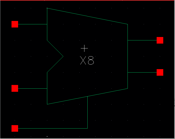
12.20 using 6u/600n devices, creating a symbol for the circuit, and
then use the symbol to create an 8-bit adder.
