This lab will focus on the layout and submission preperation to MOSIS for device fabrication.
Tutorial 6 was completed prior to the start of this lab and all content was reviewed in its entirety.
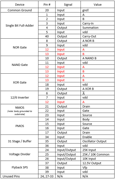
Using a 40 pin pad design, the devices listed below should be added being sure to not allow any two devices to share a vdd connection to prevent shorts to ground that would cause all devices to become inoperable. Global ground can be shared amound devices located on pin 20.
Devices Added to the Chip:
- Flyback Switching Power supply from F_20 semester
- 31-stage ring oscillator with buffer circuit to drive a 20pF off-chip load
- 6u/600n NAND, NOR, and XOR gates
- 12/6 inverter with minimum length
- 6u/600n PMOS and NMOS with all terminals connected to indivdual pins outside of global grounded NMOS
- 25K N-well resistor and 10K hi-res resistor forming a voltage divider
- Single bit full-adder
Pin
definitions, associated schematic and device locations should be
included along with a concise testing procedure to verfiy proper
operation of each device
Laboratory Procedure
Device list with pin locations shown below:
** NOTE: For many logical operations Input Pins 12 & 13 are share among devices **
Chip1_f21 Truth Table
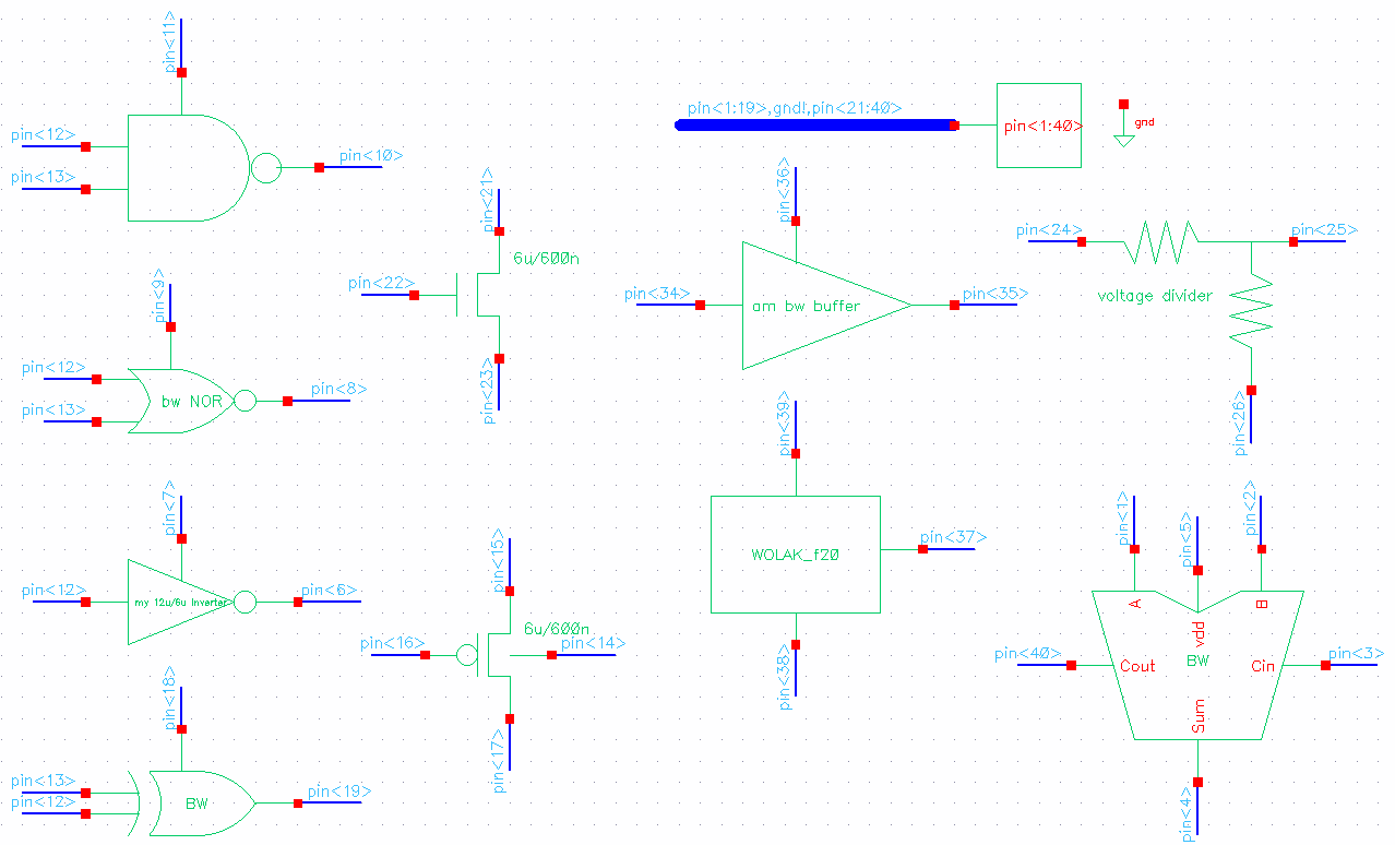
Chip1_f21 Master Schematic
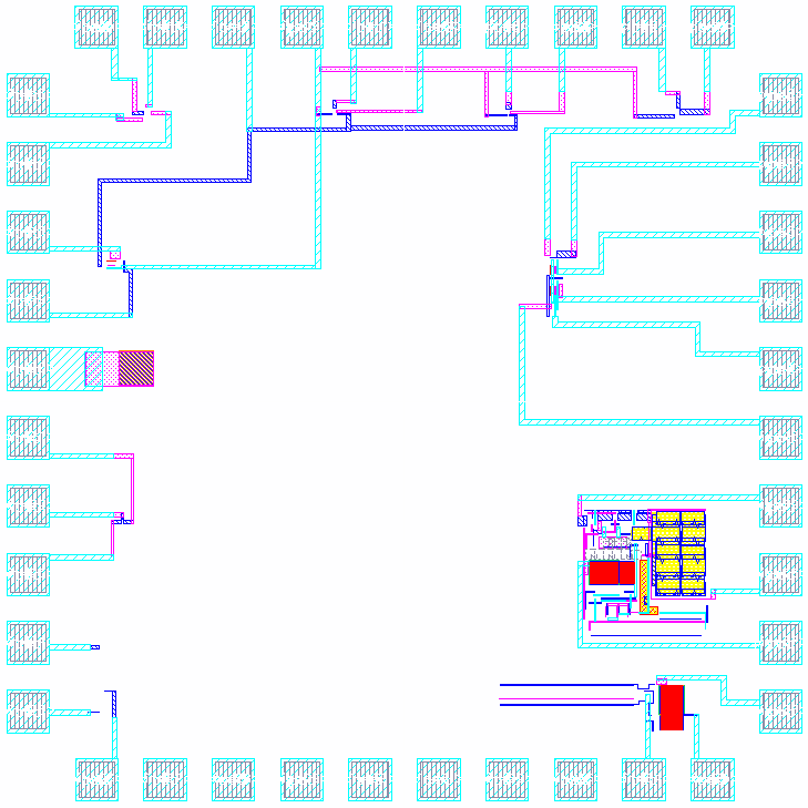
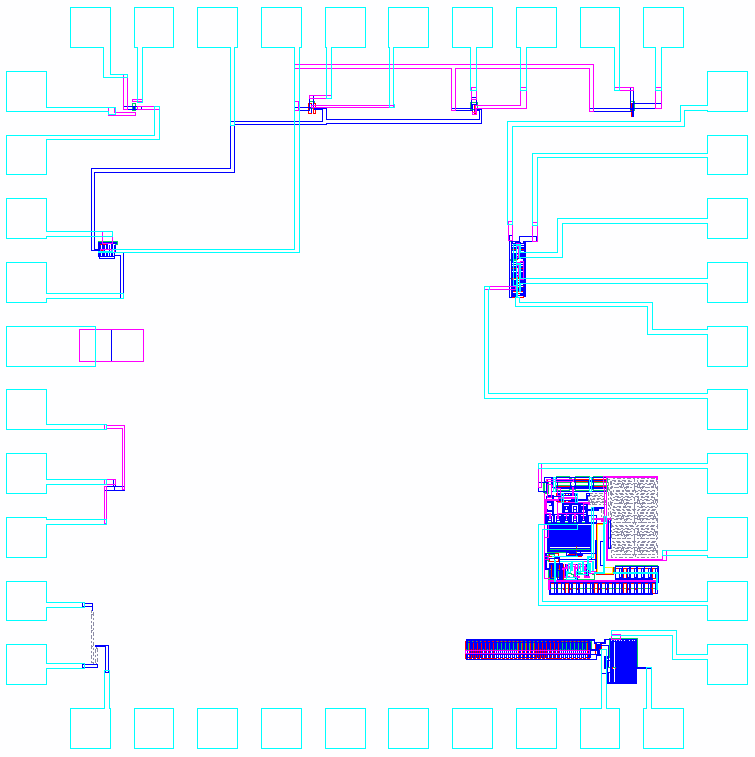
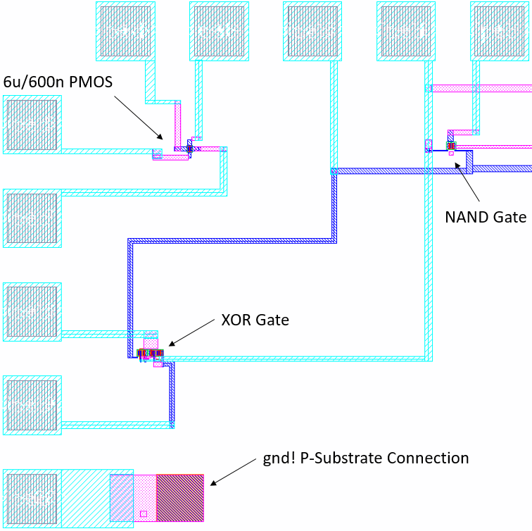
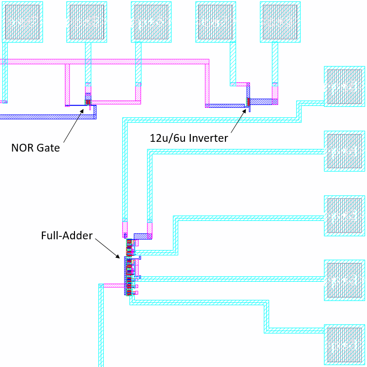
Chip1_f21 Master Layout and Extracted Views
Zoomed Views With Device Notations
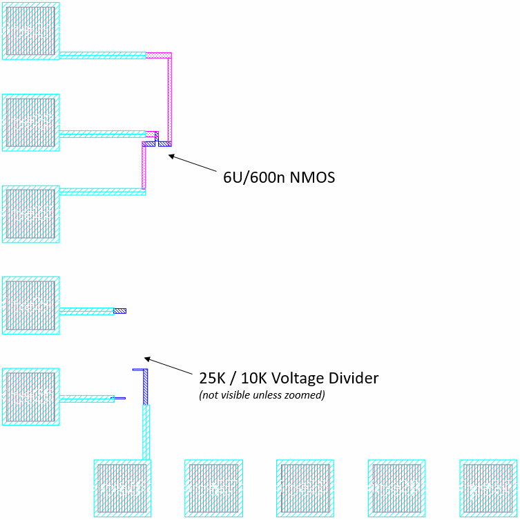
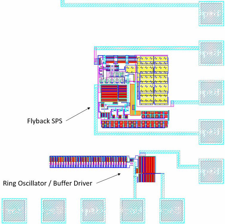
Zoomed Views of Chip1_f21

Chip1_f21 Master Layout and LVS Confirmation
Chip1_f21 Test Procedure
The following test procedure will verify proper device operation of each device located on the Chip1_f21 chip when followed correctly.
Logic Circuit Test Procedure:
Begin by applying a ground to Pin 20 (this will stay connected through the entire test procedure) and then powering up each logic device individually with a 5v vvd supply voltage one at a time using the table above while referencing the device logic truth table shown below to verify each device's output response in regards to the defined inputs. Pins 12 & 13 will as common inputs for NOR, NAND, XOR and the Inverter.
** NOTE: This is assuming a logical '1' = 5v and '0' = 0v **
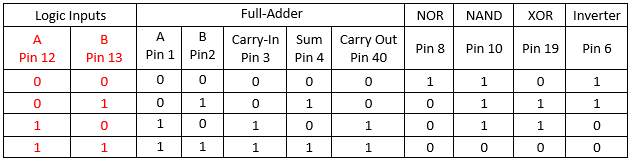
Chip1_f21 Logical Truth Table
31 Stage Ring Oscillator / Buffer Test Procedure:
Applying a 5v vdd supply to Pin 36 and Pin 34, attach a 20pF capacitor or load to Pin 35 to verify proper operation. Also verify that disconnecting Pin 34 (enable) will disable the output of Pin 35.
NMOS Test Procedure:
Applying a gnd connection to Pin 23 (source), sense the voltage at Pin 21 (drain) while applying a 5v vdd voltage to Pin 22 (gate), the NMOS will act as a switch when 5v vdd is applied to the gate bringing Pin 21 to ground.
PMOS Test Procedure:
Applying a 5v vdd voltage to Pin 15 (source), ground Pin 22 (gate) while sensing the voltage output to Pin 23 (drain). Pin 23 will be drawn to 5v vdd as the PMOS acts as a switch when the gate is grounded.
25K / 10K Resistor Test Procedure:
Using a multimeter, measure resistance across Pins 24 & 25. Reading should be close to the expected 25K ohms. Then measure across Pins 25 & 26. Resistance should be as expected near 10K ohms.
Flyback SPS Test Procedure:
Create the following circuit provided below attaching to Pins 37-39 and verify 12.5V output voltage on Pin 37.
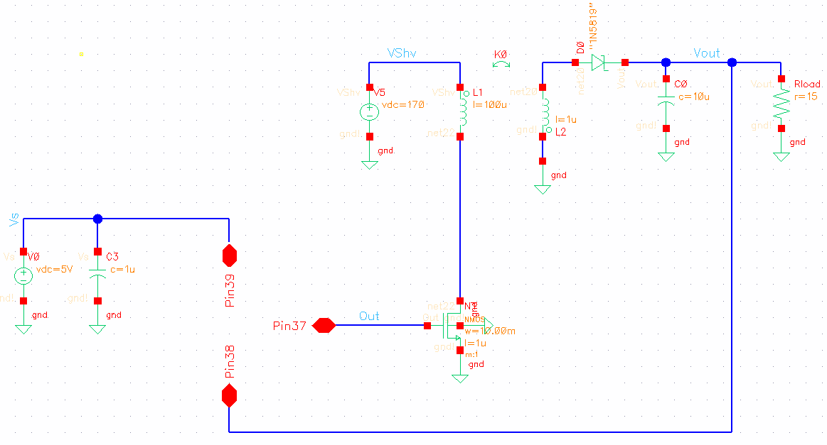
Flyback SPS Test Circuit
At any point in the testing procedure Pin 20 can be disonnected at any moment disabling all functionality of the chip and internal devices.
This concludes the testing procedure.