Lab 7 - EE 421L
Authored
by Adrian Lopez-Macuaran,
lopezmac@unlv.nevada.edu
October 26, 2021
Lab
description
Design, layout, and simulate of a CMOS Nand gate, Xor gate, and Full-Adder
Pre-Lab
- Back-up all of your work from the lab and the course.
- Go through Tutorial 5 seen here.
- Read through the entire lab before starting it.
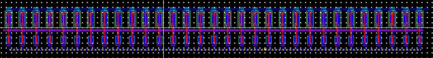
Completing Tutorial 5, we are going to design a 31 stage ring oscillator.
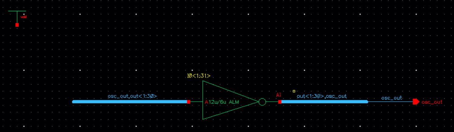 The
blue wiring are called busses and are used to avoid using mutiple
inverters. The following images will show the Layout,DRC,Extract, and
LVS of the ring oscillator.
The
blue wiring are called busses and are used to avoid using mutiple
inverters. The following images will show the Layout,DRC,Extract, and
LVS of the ring oscillator.
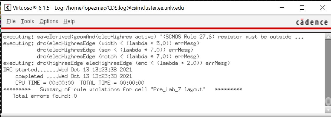
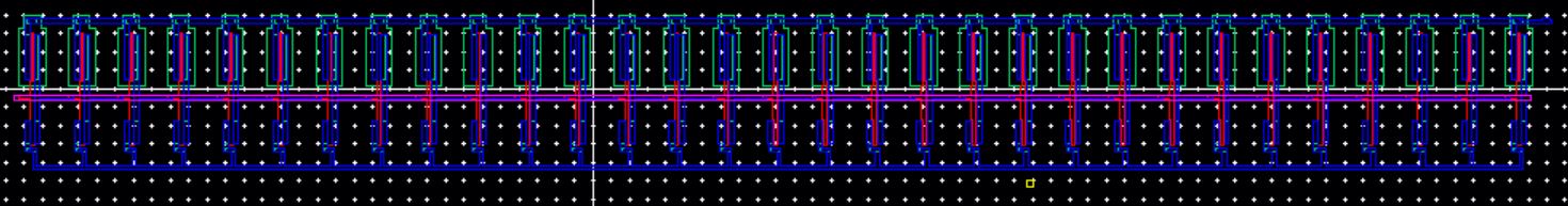
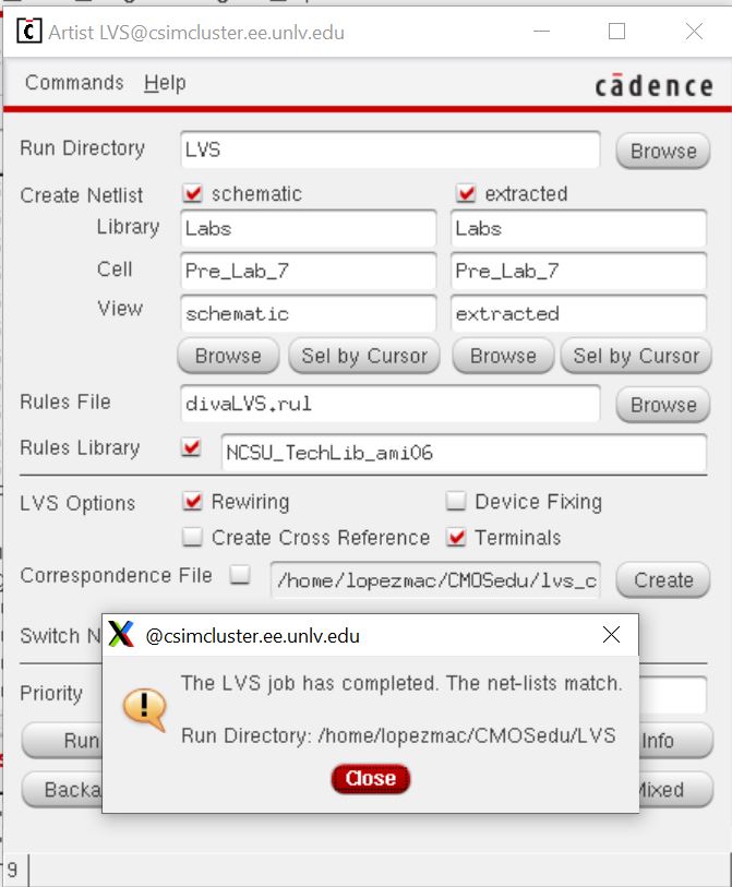
As
seen above my design was completed with zeor erros in the drc and
passing LVS. The following will show my graph for the oscillator.
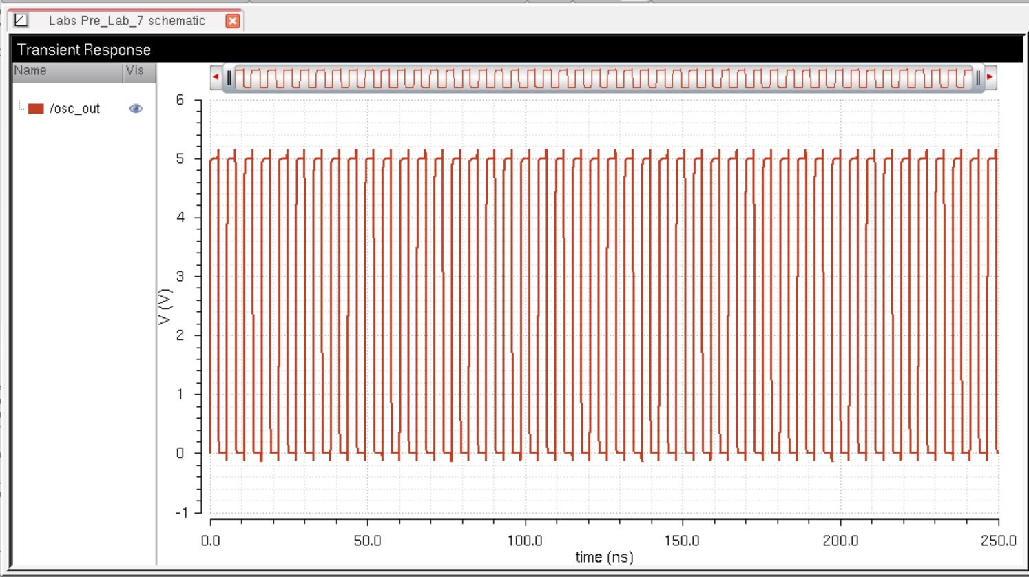
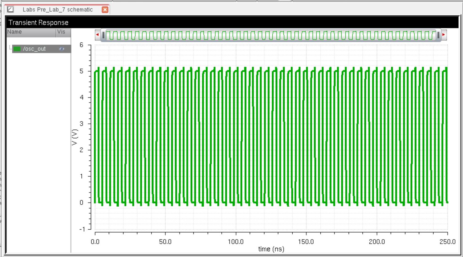
Next I will show the graph using the extracted in my design enviroment.
 Main Lab Content:
Lab task 1:
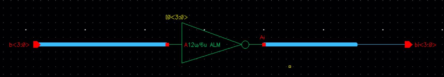
Creat a 4-bit word inverter:
First
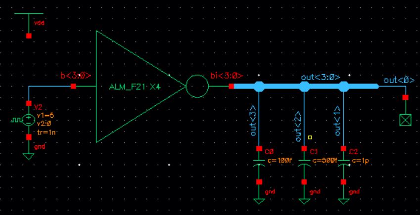
we are tasked with making a 4-bit word inverter using 6u/0.6u
transistors. Then we need to attach the outputs to loads as specified:
- The out<0> is not connected to a load while out<3> is connected to a 100fF load.
- The out<1> is connected to a 1 pF load while out<2> is connected to a 500 fF load.
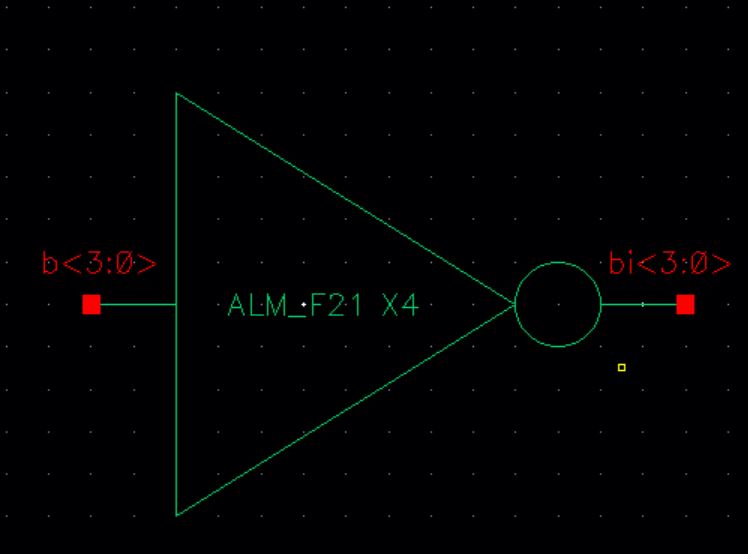
First I will show the schematic and symbol.
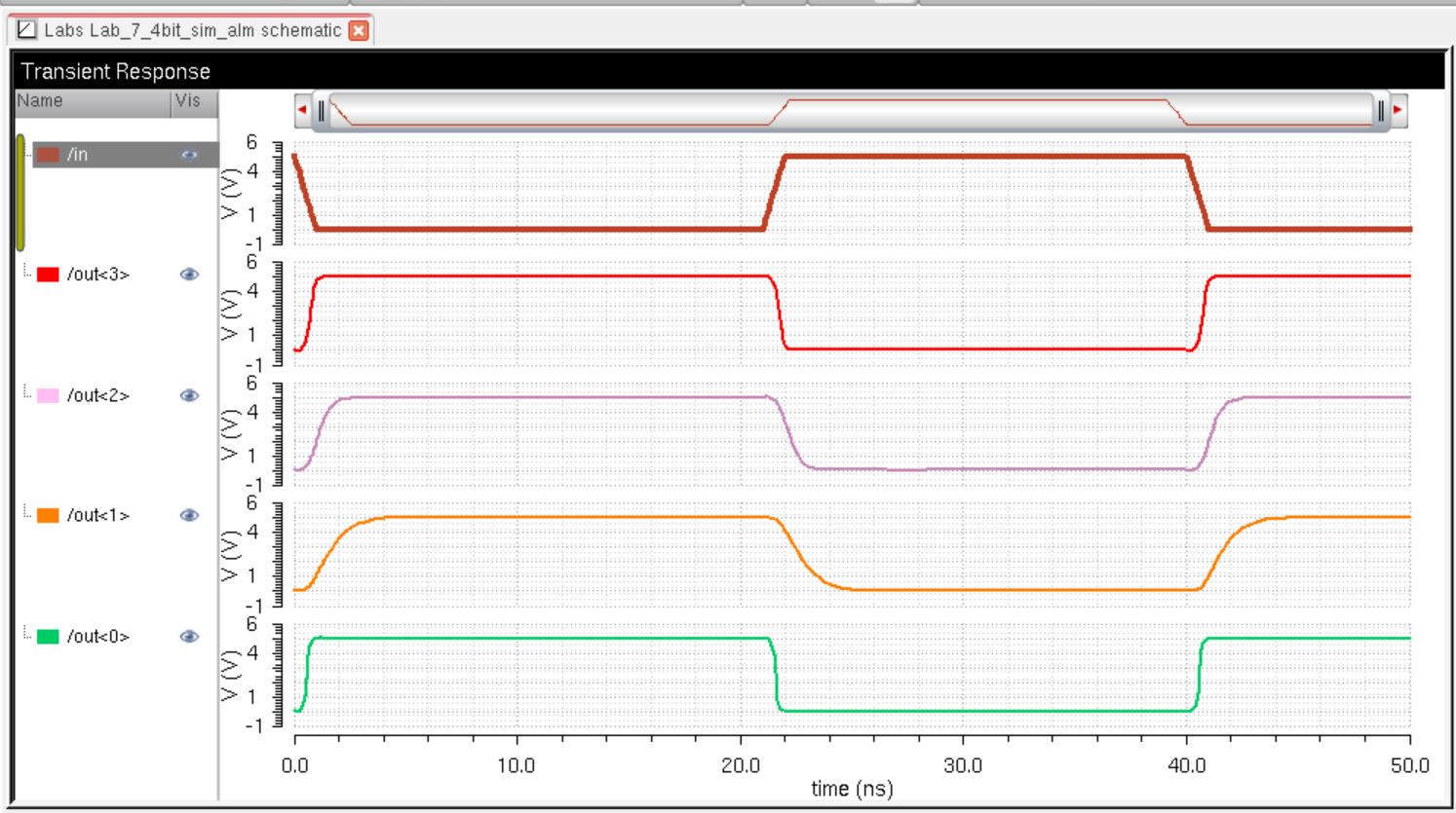
Next using the new symbol I will show the schemactic and graph results.
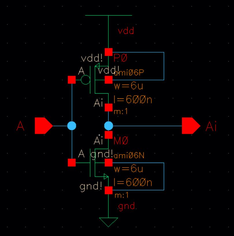
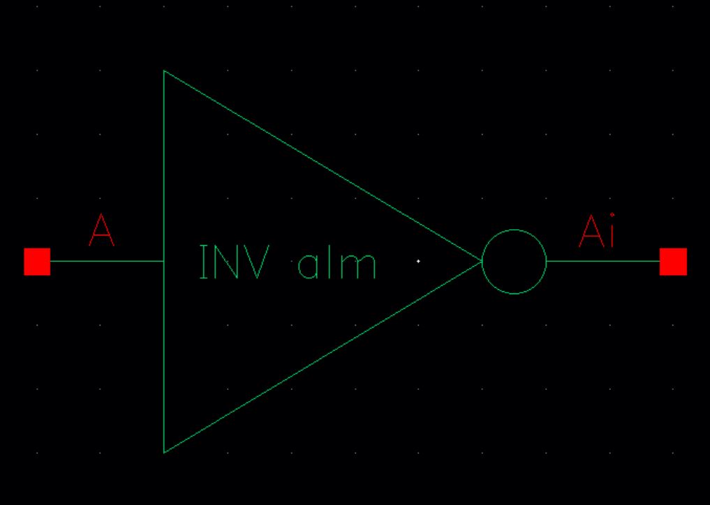
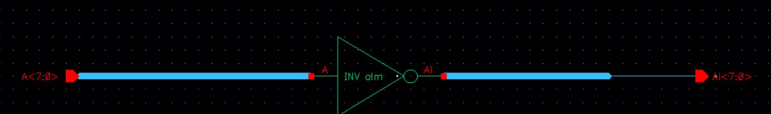
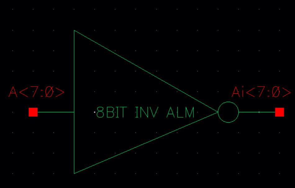
Next I will show the 8bit I/O Inverter. I will show the schematic and symbol.
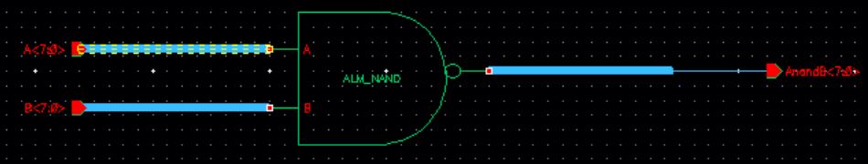
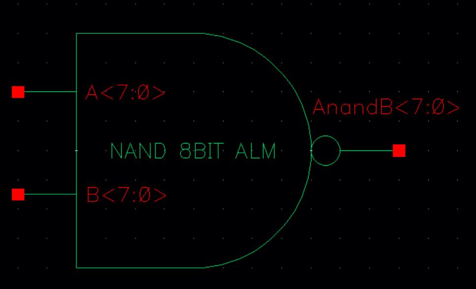
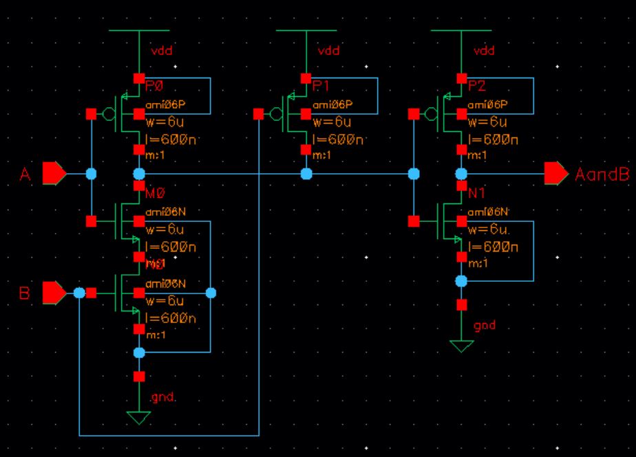
Next
I will show the 8 bit I/O Nand gate with the schematis and symbols. For
this one symbol I used the schematic and symbol from the preivous
lab
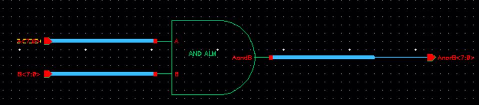
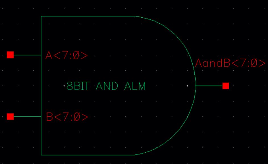
Next I will show the 8 bit I/O AND gate with the schematis and symbols.
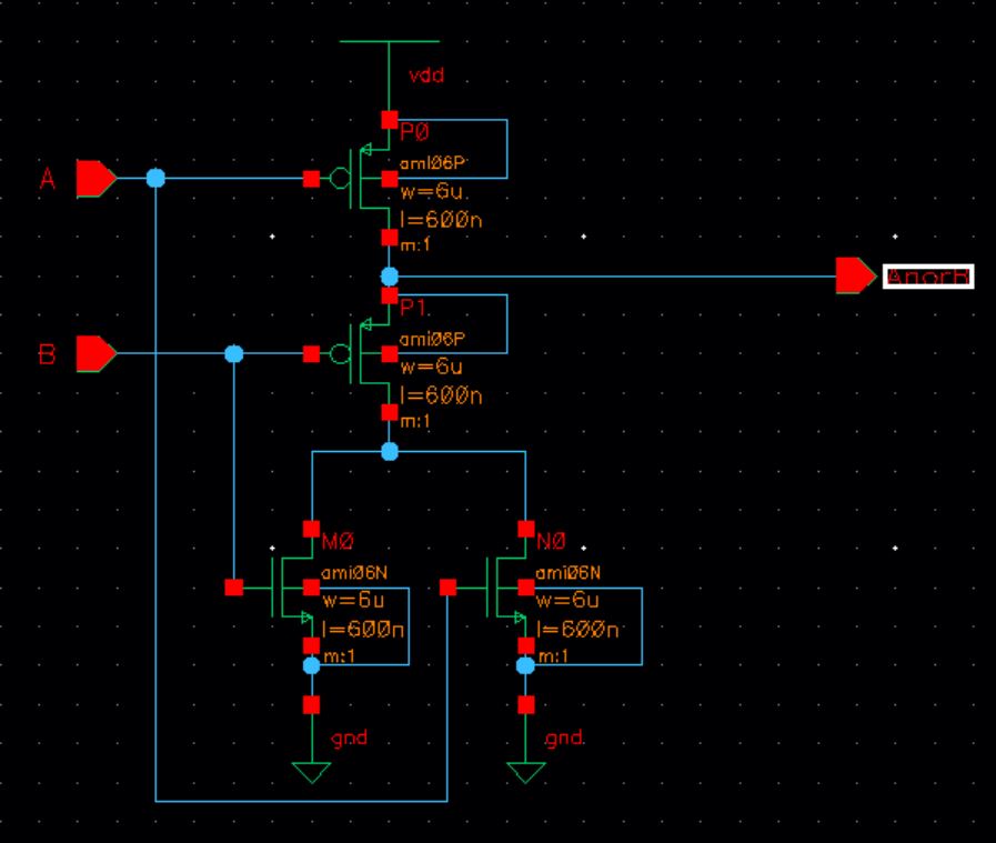
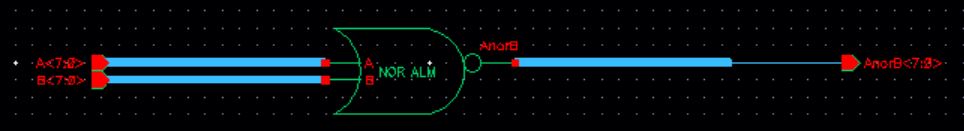
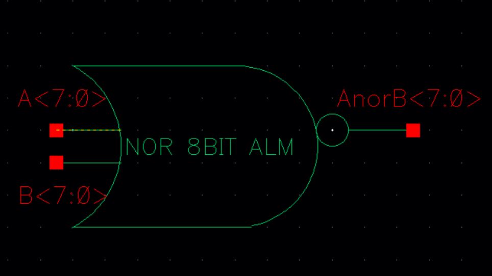
Next I will show the 8 bit I/O NOR gate with the schematis and symbols.
\
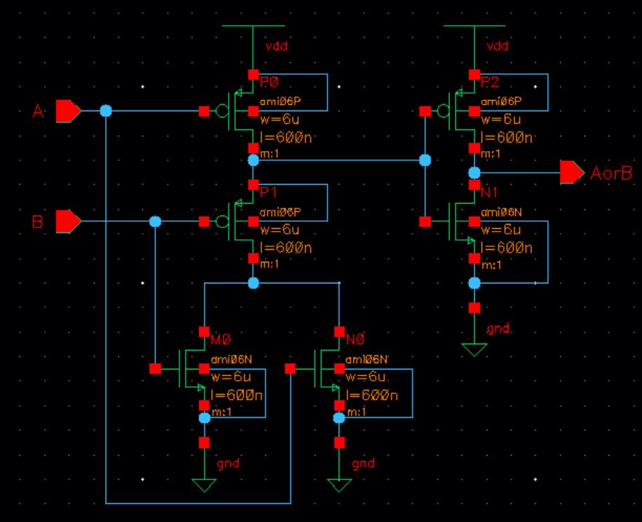
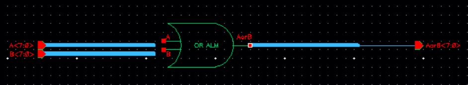
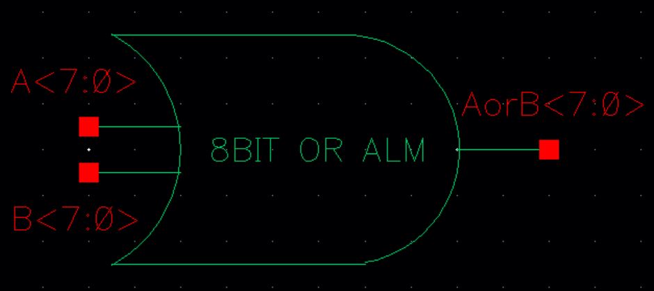
Next I will show the 8 bit I/O OR gate with the schematis and symbols
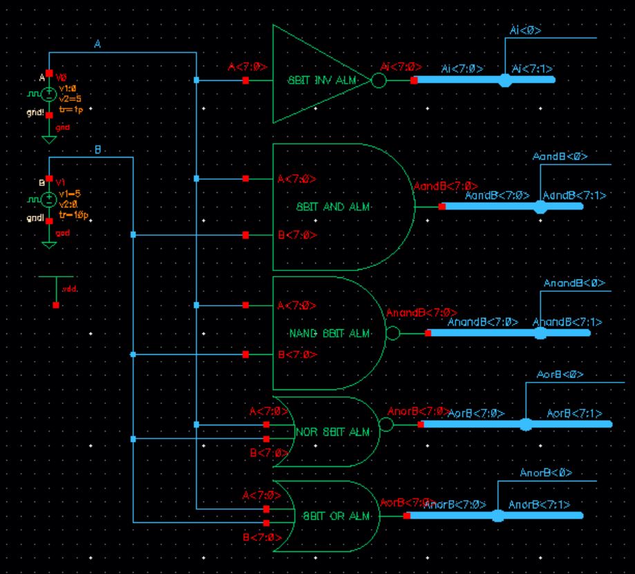
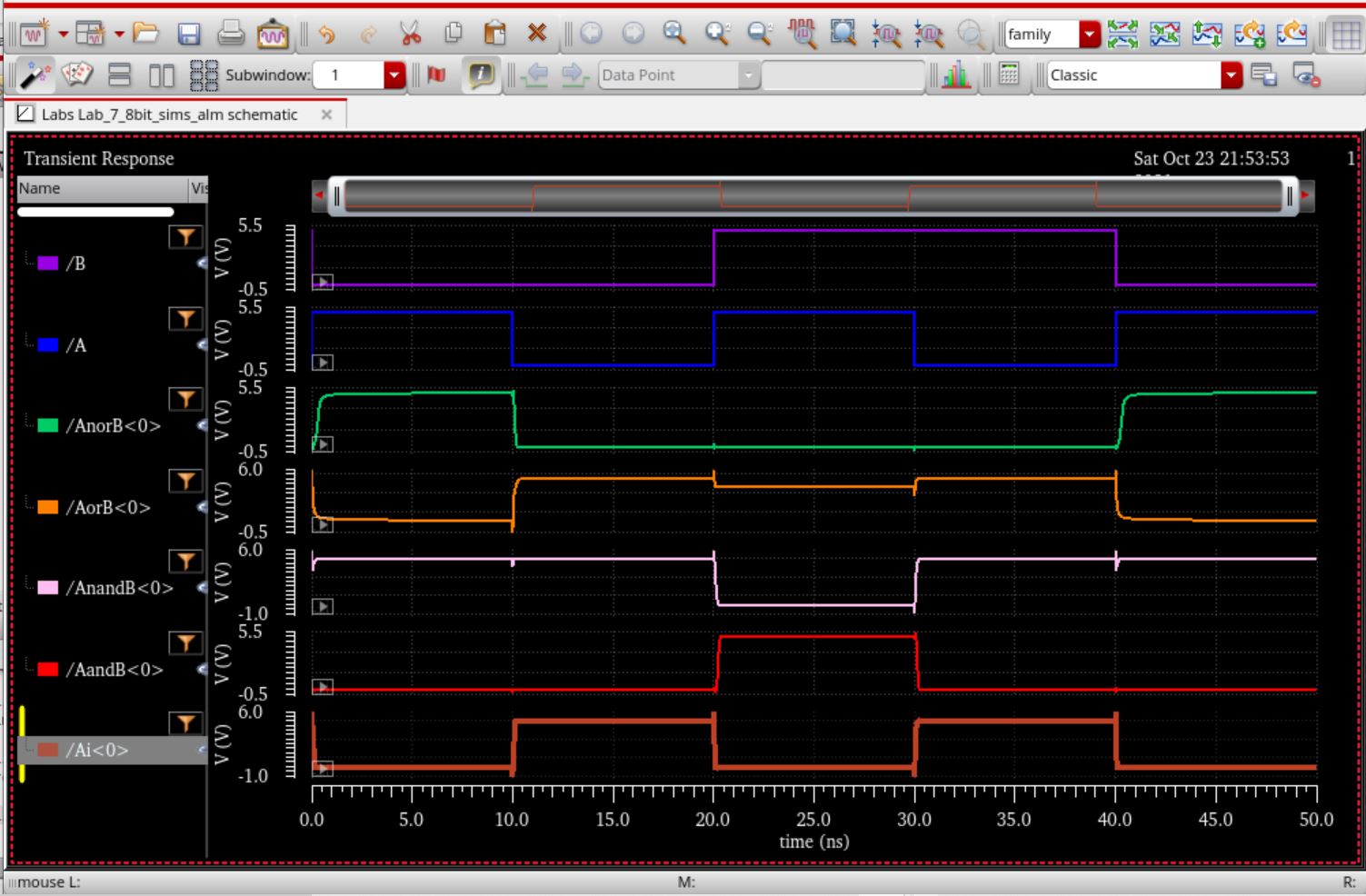
Next
I will test all the symbols and make sure they are working correctly to
save time I will simulate all the logic gates at one time.
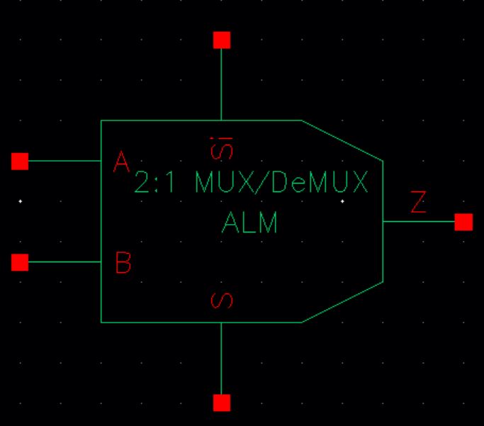
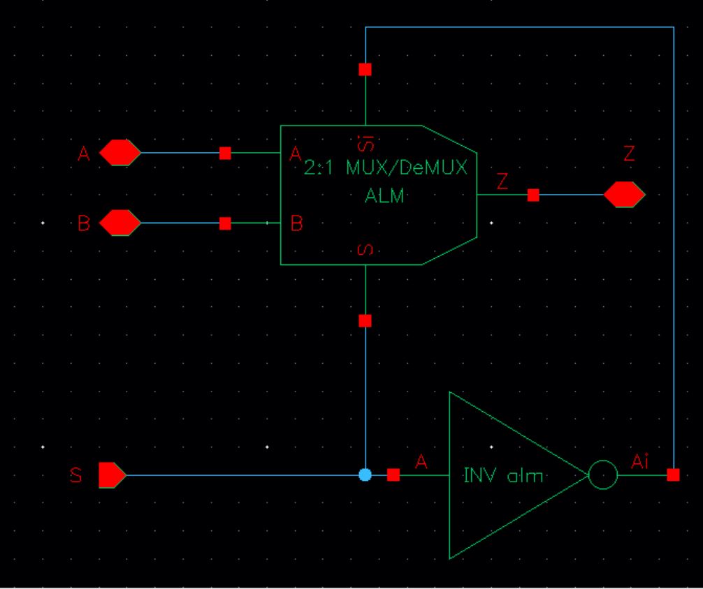
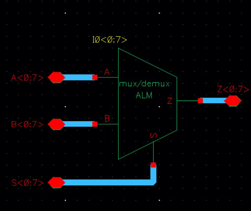
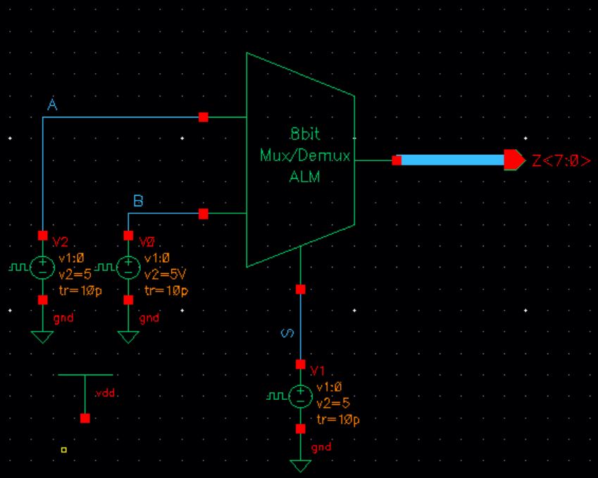
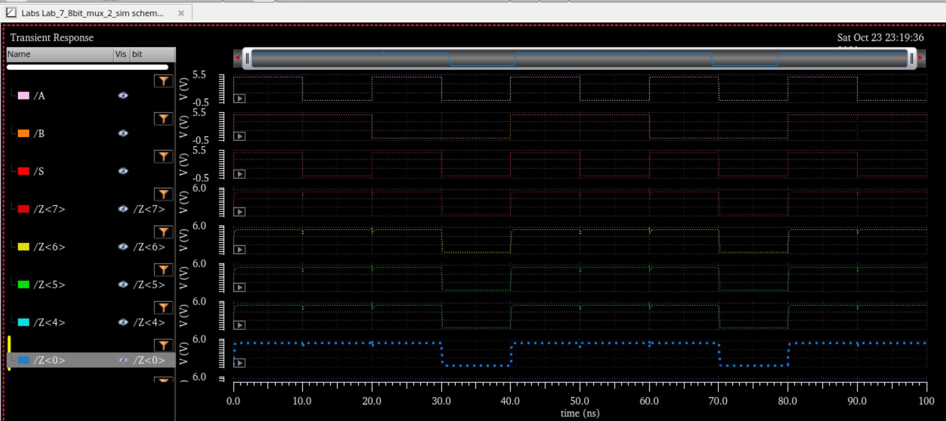
Next I will show the 2:1 MUX with the schematis, symbol, and graph.
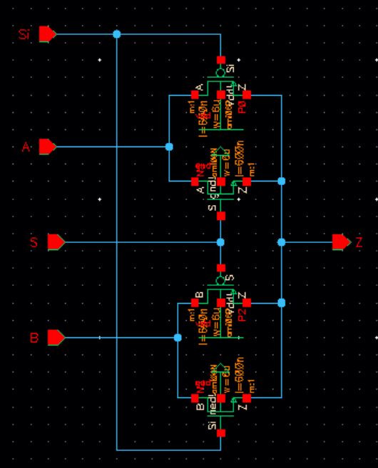
From
the graph we can tell that when S is high, then all of the ouputs
follow A input. Is S is low then all of the ouputs follow B.
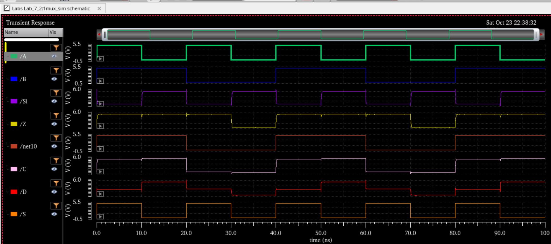
2:1 MUX/DEMUX
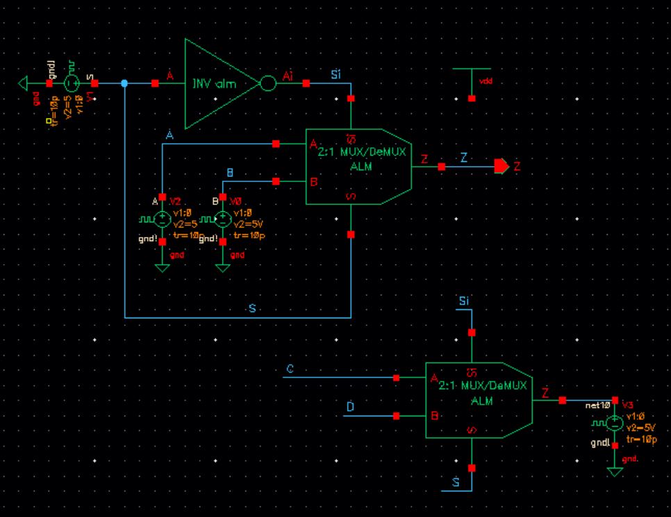
The
mux acts the same in this graph as in previous. The DEMUX when S is
high the input signal Y only goes to C and if S is low then the input
signal goes to D.
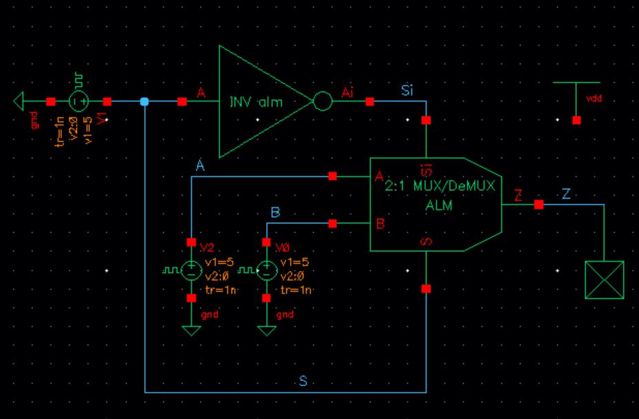
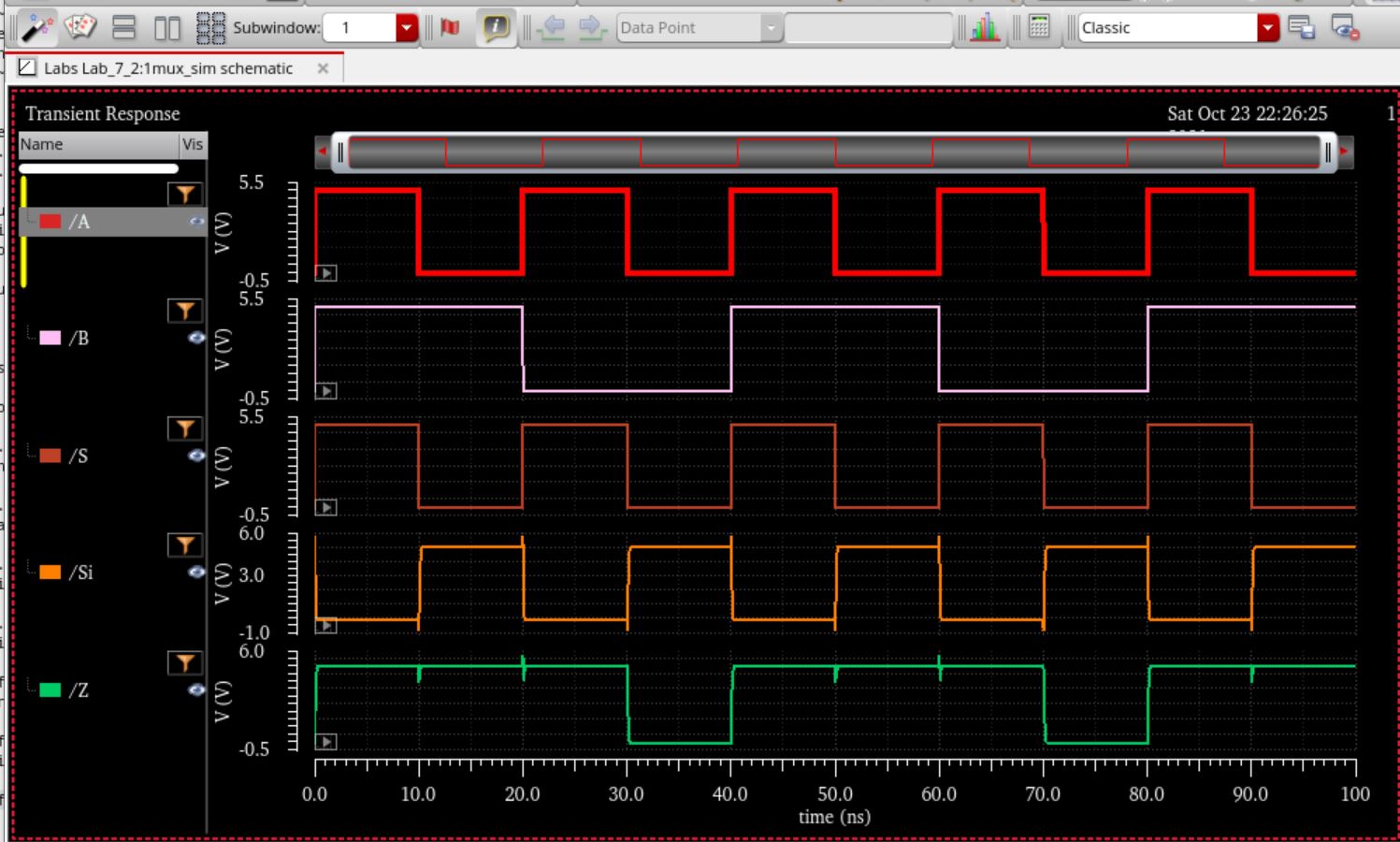
2:1 MUX with single select input
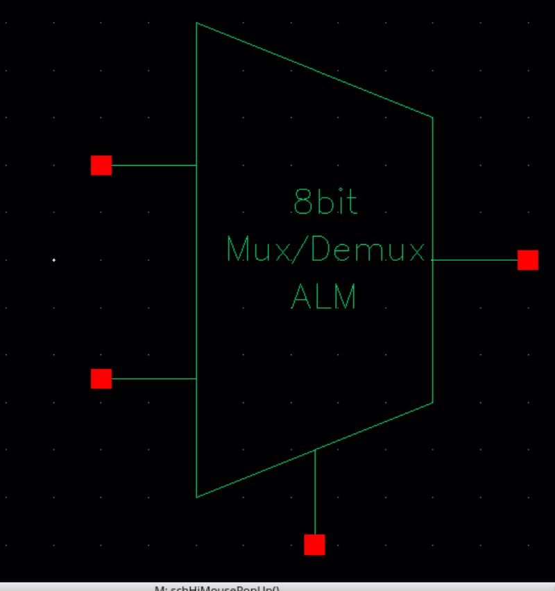
When S is high all of the ouputs follow A and if S is low then all ouputs follow B.
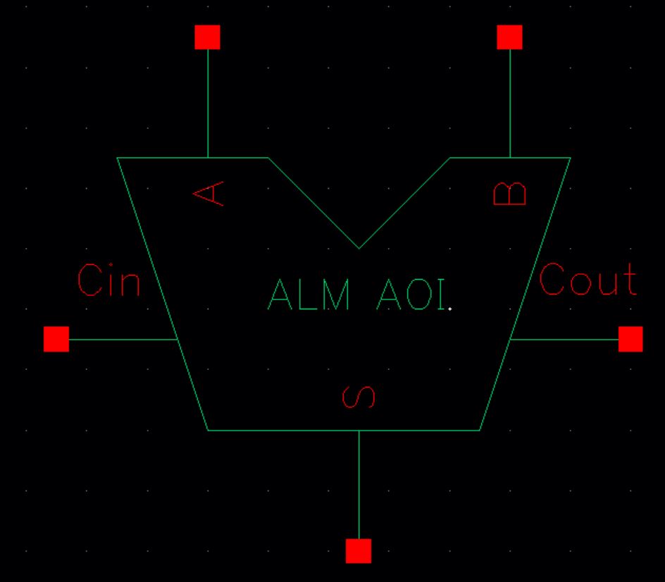
AOI Full Adder. I followed the scheamtic found in theCMOS book, figure 12.20.
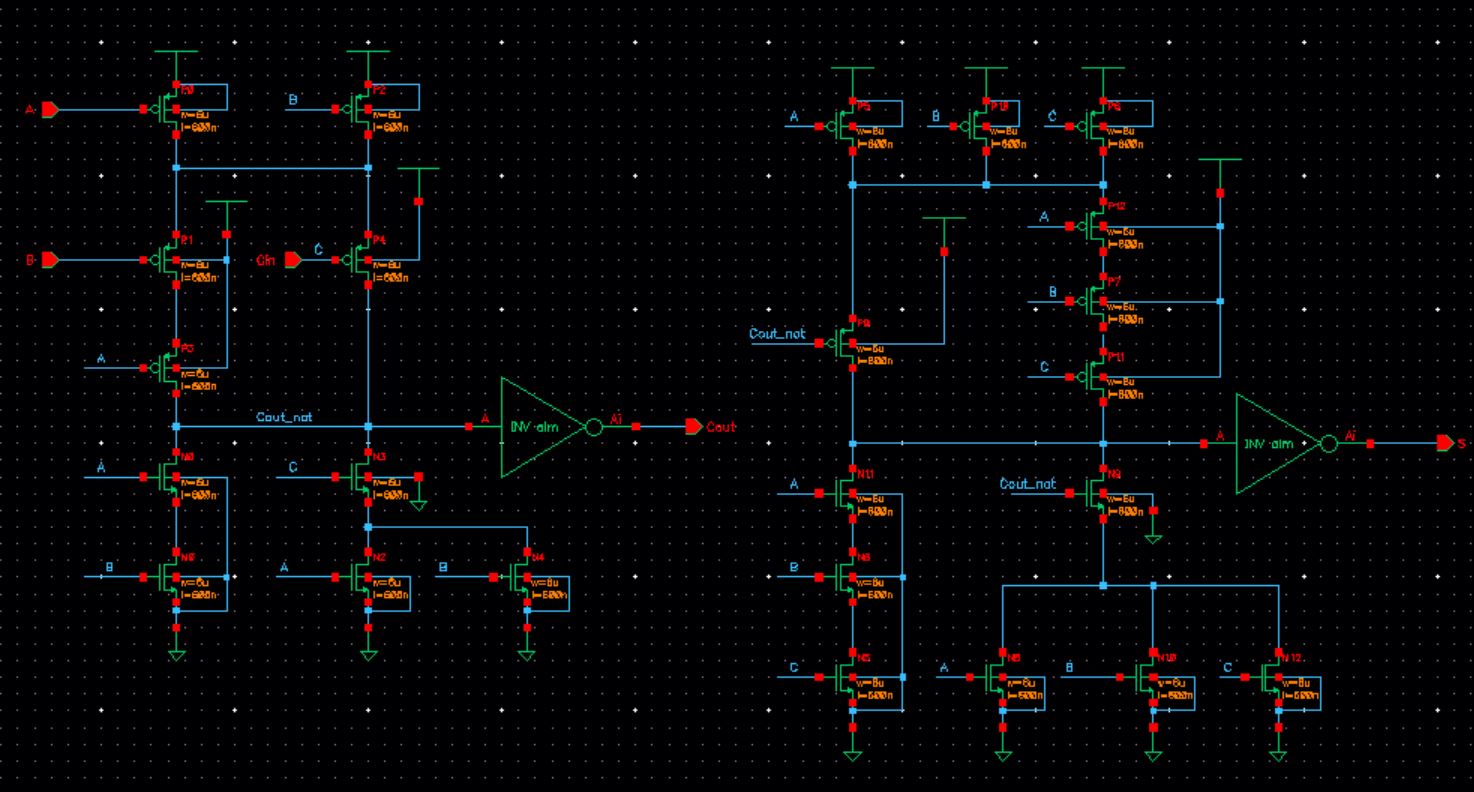
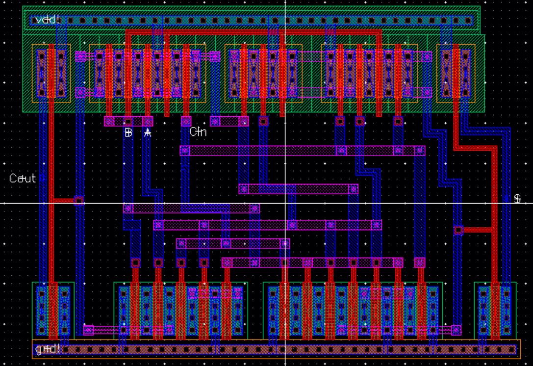
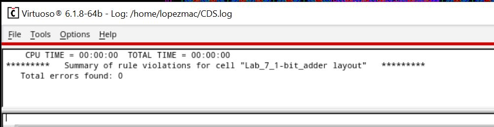
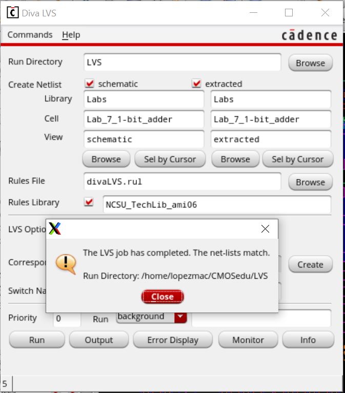
Next I will show the Layout,DRC, and LVS of the single bit Full Adder.
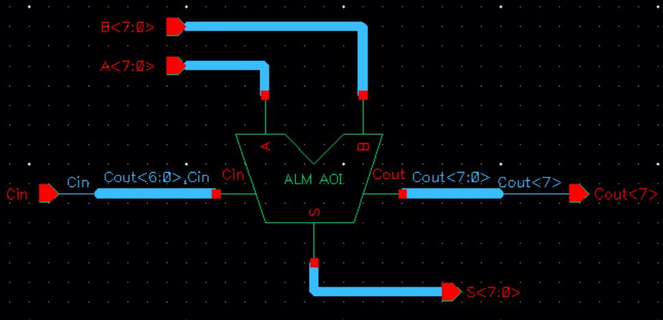
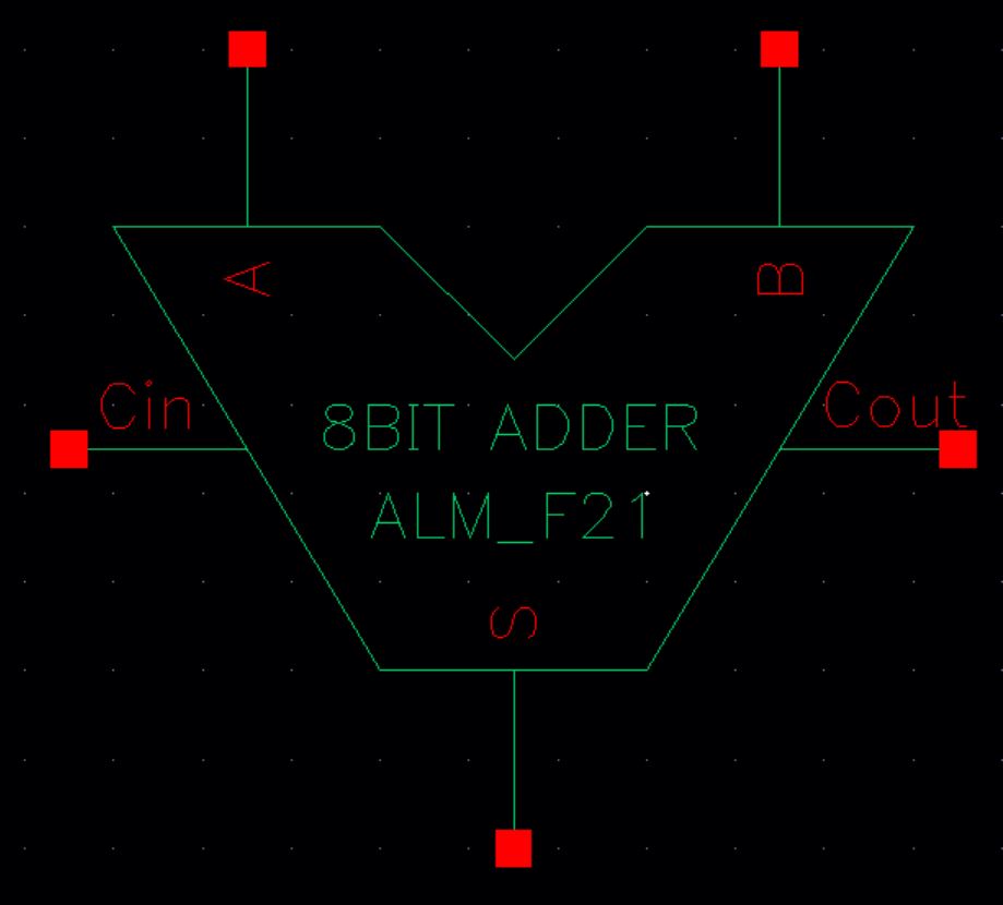
Next I will show the 8 bit AOI Full Adder.
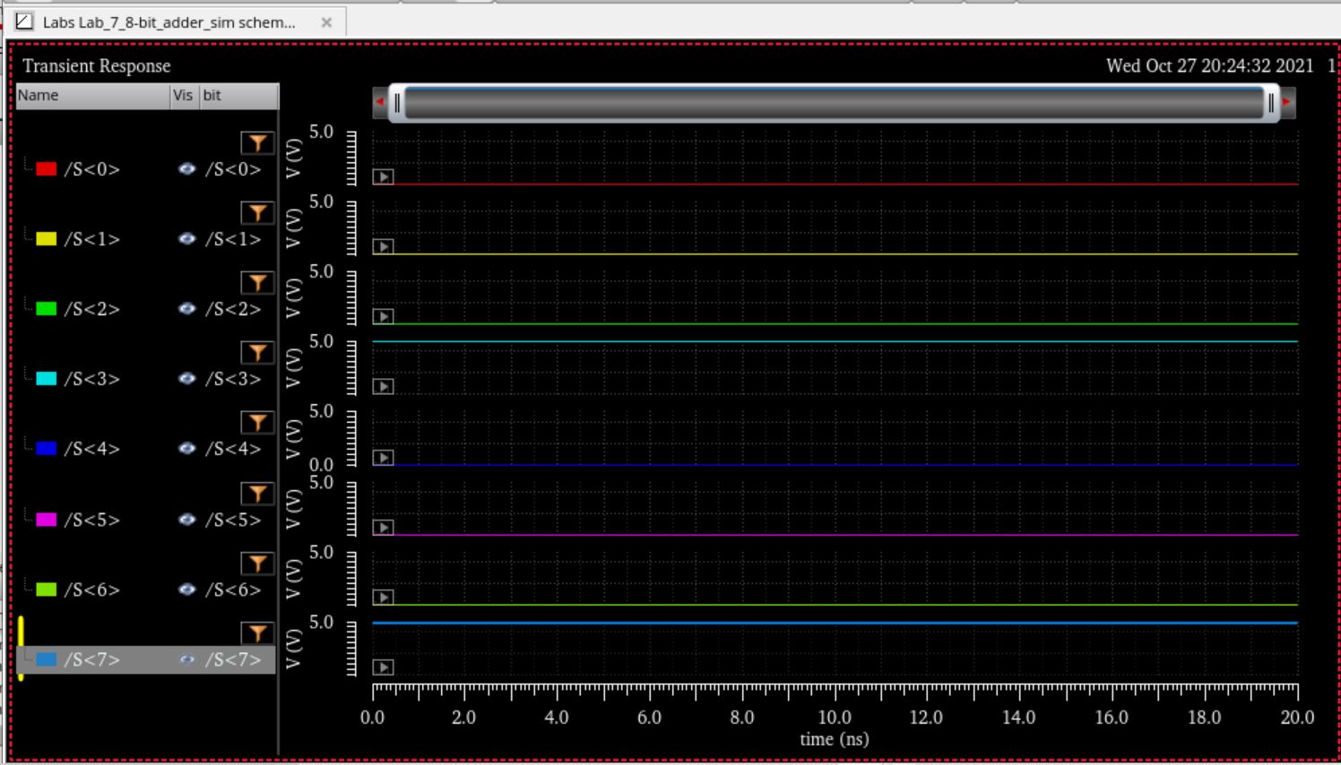
Next I will show the 8bit Full Adder Sims then I will show the layout,DRC, and LVS.
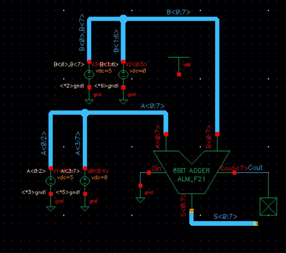
The following will show the graph is correct by taking two 8bit numbers and adding them to produce a 8bit sum with no carry in.\
A = 00000111 = 7
B = 10000001 = 129
S = 10001000 = 136
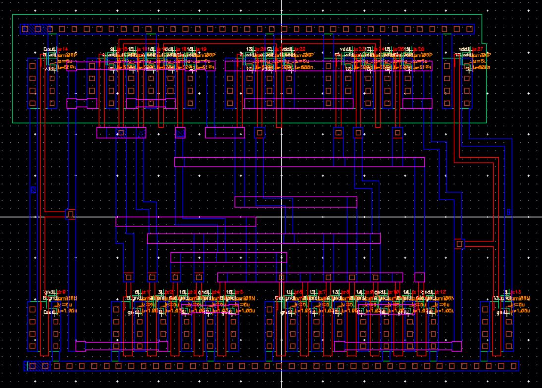
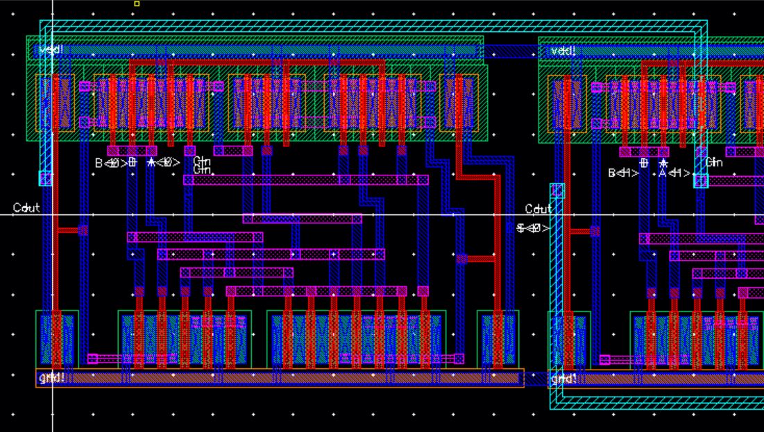
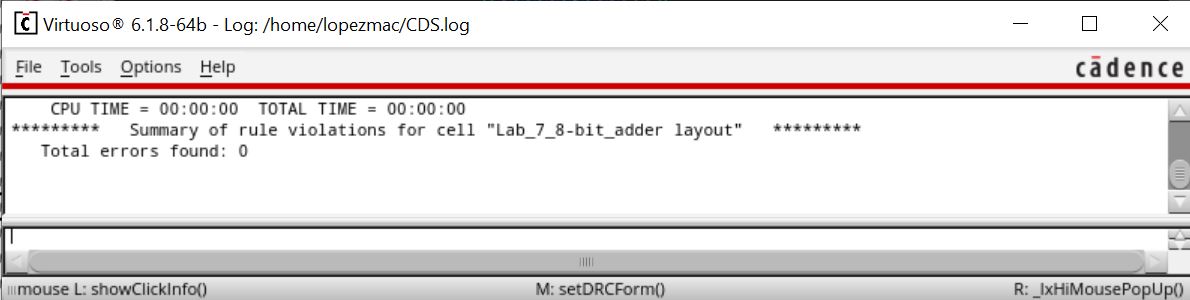
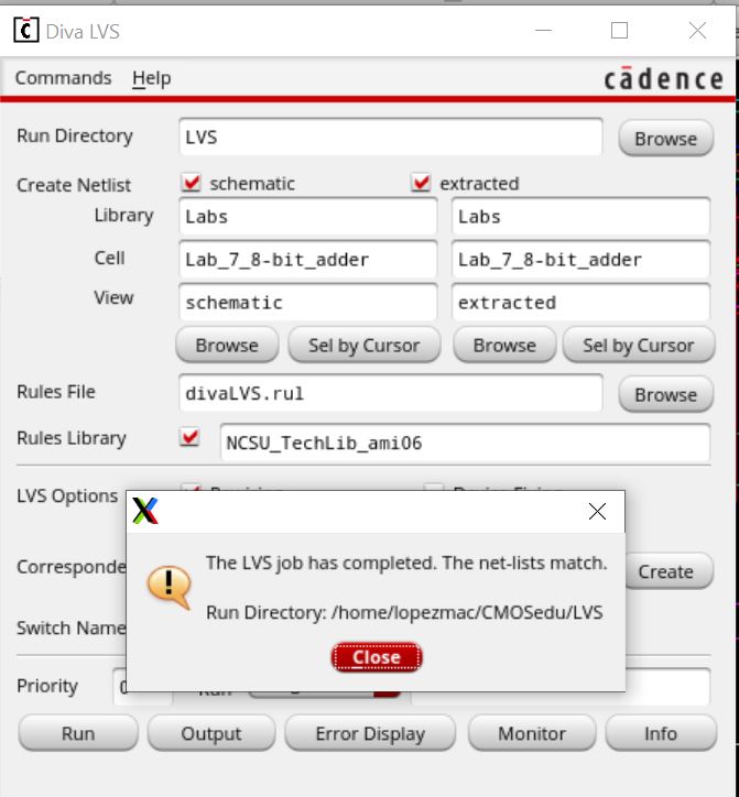
Next
I will show the 8bit full adder layout,DRC, and Lvs. The first image
will be zoomed in. I instanciated each 1bit adder to make this so that
is why you can see some double names appear such as the CIN. This did
not affect my desing. The tricky part was only labling Cout<7>
and not Cout<7:0>.
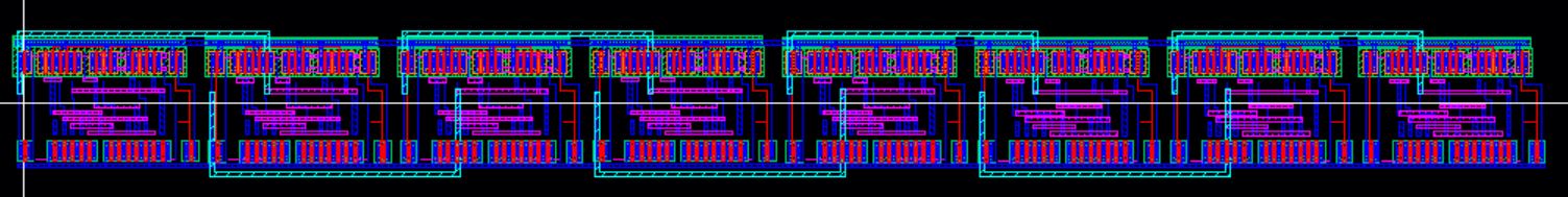
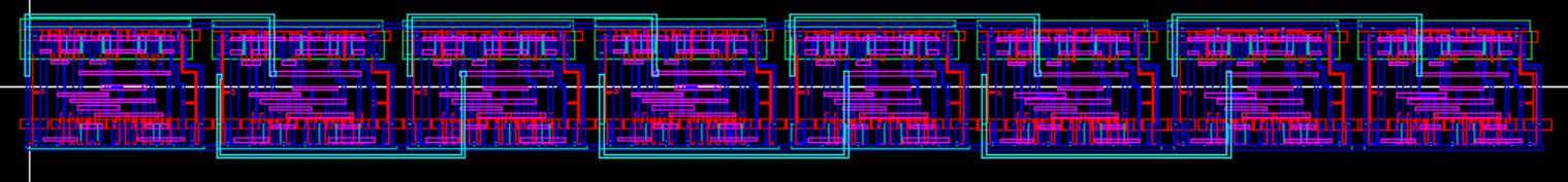
Full Layout
This concludes lab 7.
Backing up work
As always I backed up work as I worked through the lab.
Return to Labs