Lab 6 - EE 421L
Authored
by Adrian Lopez-Macuaran,
lopezmac@unlv.nevada.edu
October 9, 2021
Lab
description
Design, layout, and simulate of a CMOS Nand gate, Xor gate, and Full-Adder
Pre-lab
- Go through Cadence Tutorial 4 seen here.
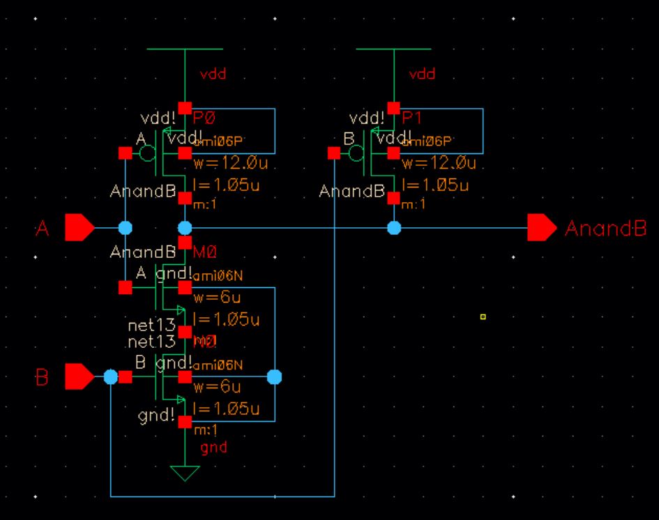
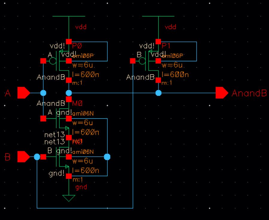
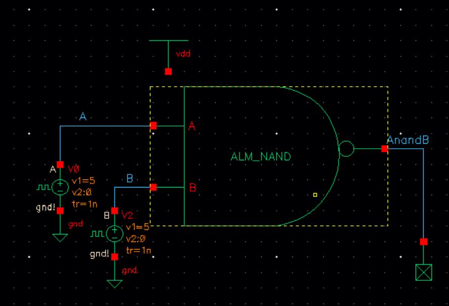
The pre-lab consist of designing a Nand gate and testing it. We will start with the NAND schematic and symbol.
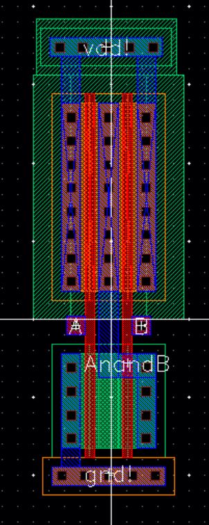
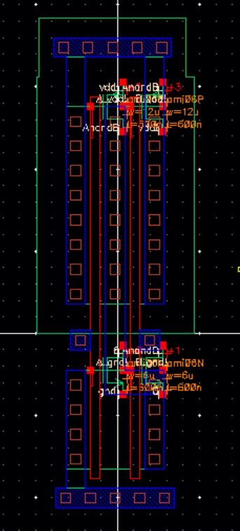
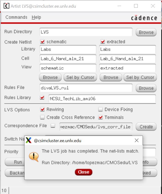
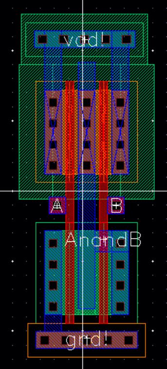
Next I will show the the layout,LVS,and extracted view.
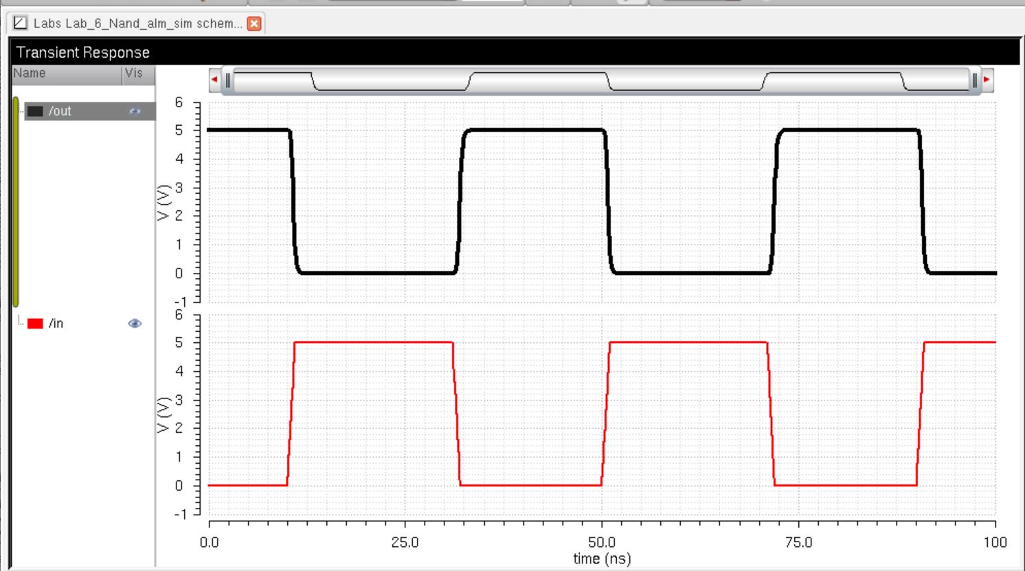
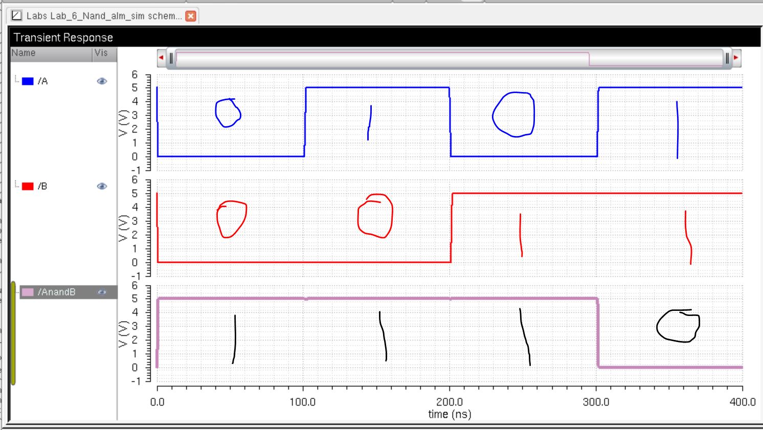
Next I weill show the simulation results.
This concludes the prelab.
Lab Tasks
- Draft
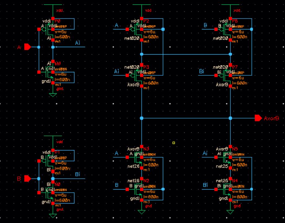
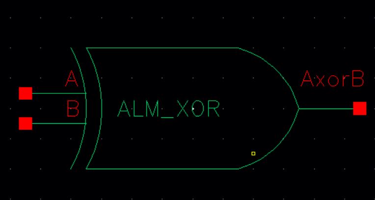
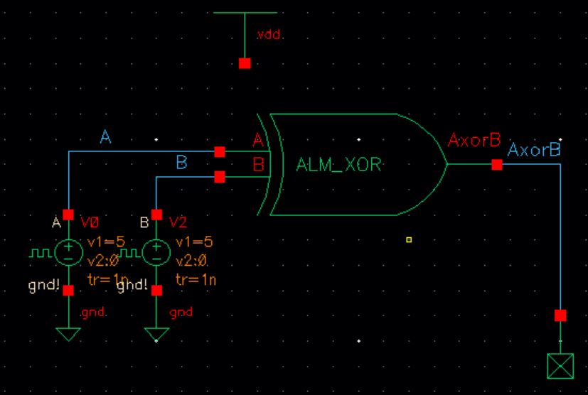
the schematics of a 2-input NAND gate (Fig. 12.1), and a 2-input XOR
gate (Fig. 12.18) using 6u/0.6u MOSFETs (both NMOS and PMOS)
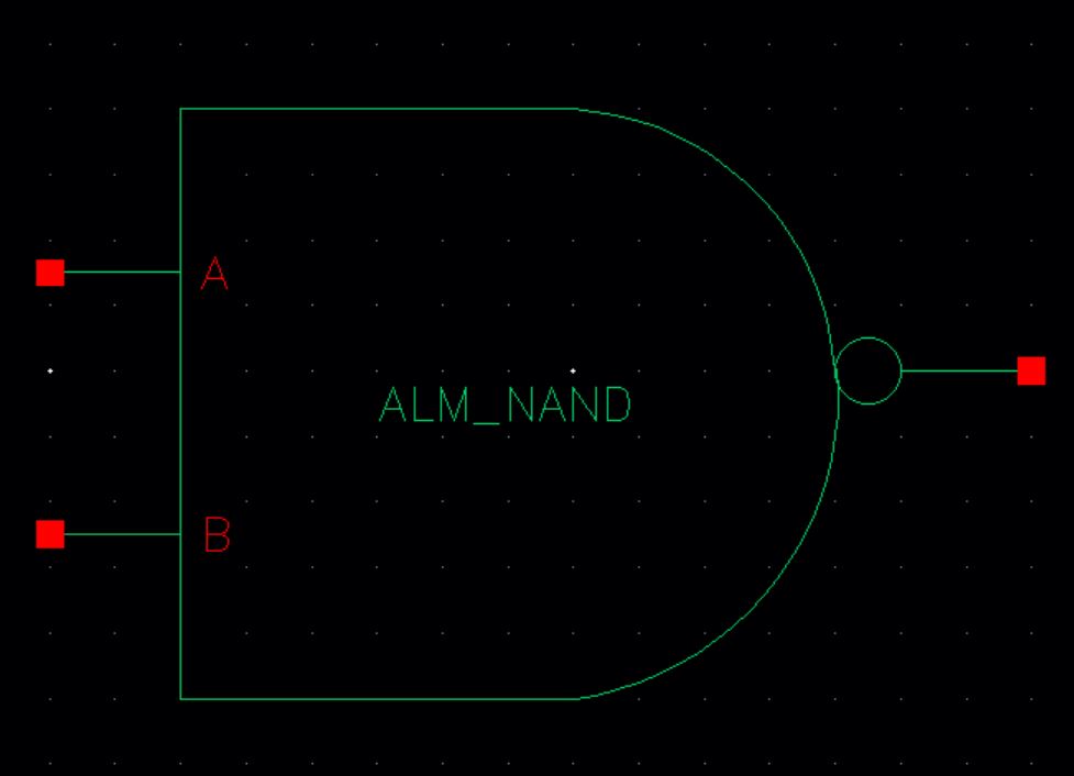
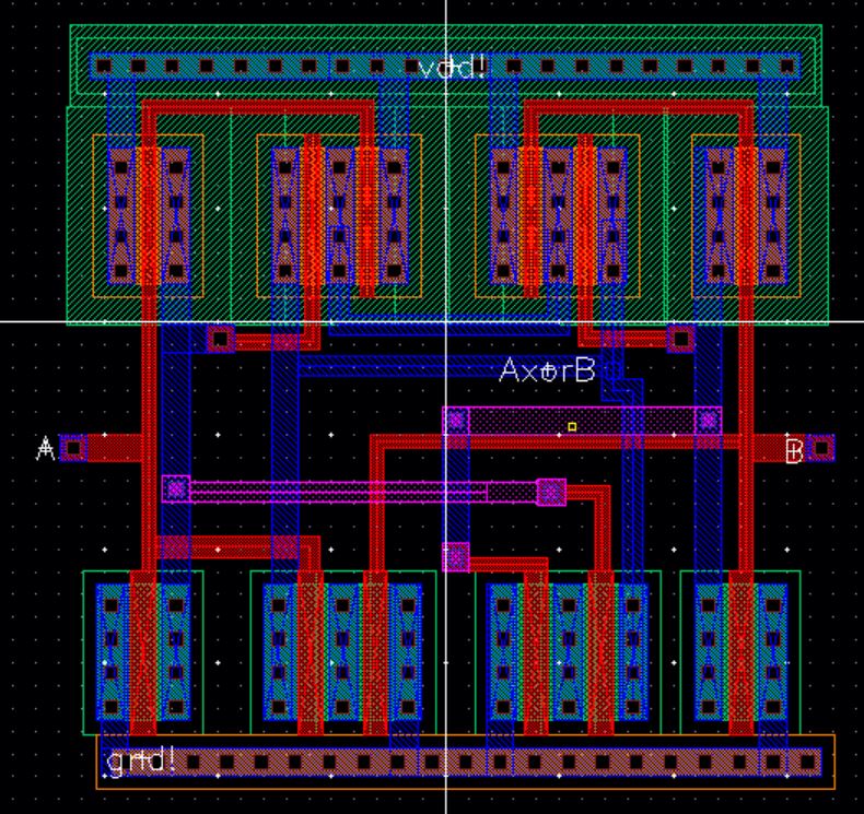
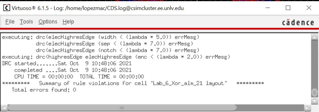
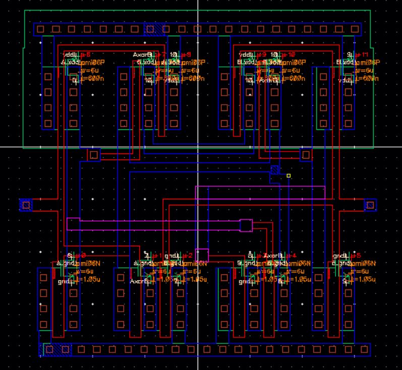
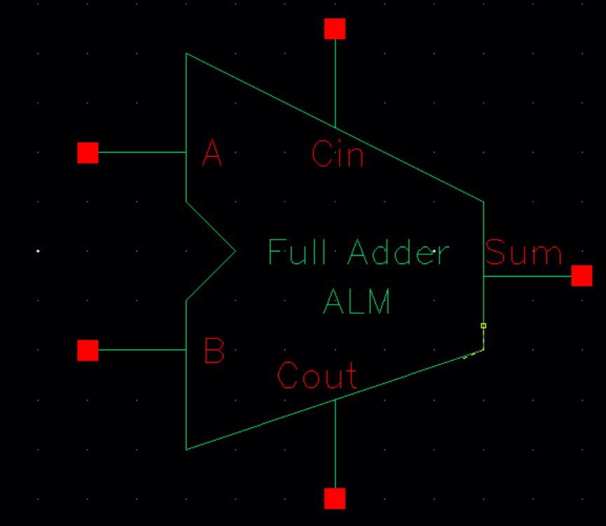
- Create layout and symbol views for these gates showing that the cells DRC and LVS without errors
- ensure
that your symbol views are the commonly used symbols (not boxes!) for
these gates with your initials in the middle of the symbol
- ensure all layouts in this lab use standard cell frames that snap together end-to-end for routing vdd! and gnd!
- use a standard cell height taller than you need for these gates so that it can be used for more complicated layouts in the future
- ensure gate inputs, outputs, vdd!, and gnd! are all routed on metal1
- Use cell names that include your initials and the current year/semester, e.g. NAND_jb_f19 (if it were fall 2019)
- Using Spectre simulate the logical operation of the gates for all 4 possible inputs (00, 01, 10, and 11)
- comment on how timing of the input pulses can cause glitches in the output of a gate
- Your html lab report should detail each of these efforts
- Below
shows (click for a larger image): 1) schematic of a 2-input NAND gate,
2) schematic of a 2-input XOR gate, 3) simulation schematic, 4) example
pulse statement to generate a digital input, and 5) simulating the
operation of the gates for all 4 possible inputs.
Frist
we will start with designing the NAND gate. Since we did this already
in prelab it was quick todo, the difference is the sizes of the PMOS
and NMOS.
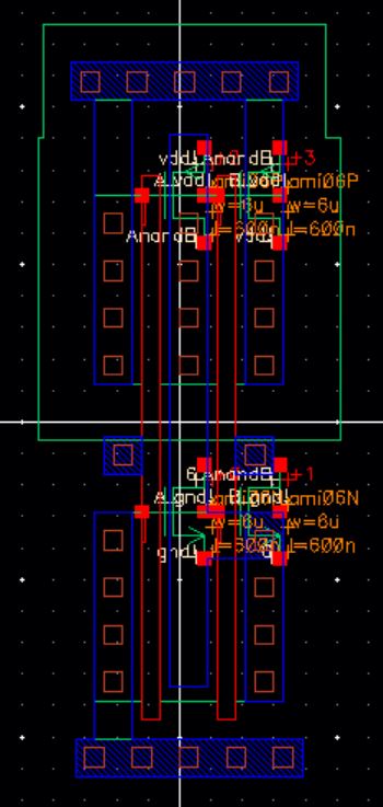
Next I will show the Layout, LVS, and extracted view of the NAND gate.
Nexg we will test our NAND gate.
Next
for the lab we will desing the XOR gate the schematic was straight
forward where I ran into during the layout and took somethinking to
finally get everything to work.
Next I will show the Layout, Drc, LVS, and extracted view of the XOR gate.
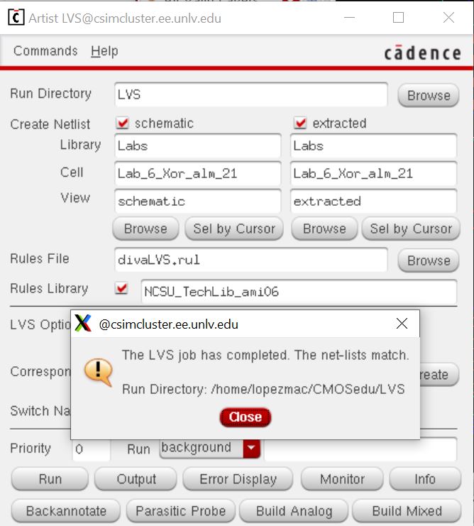
Next I will test the XOR gate.

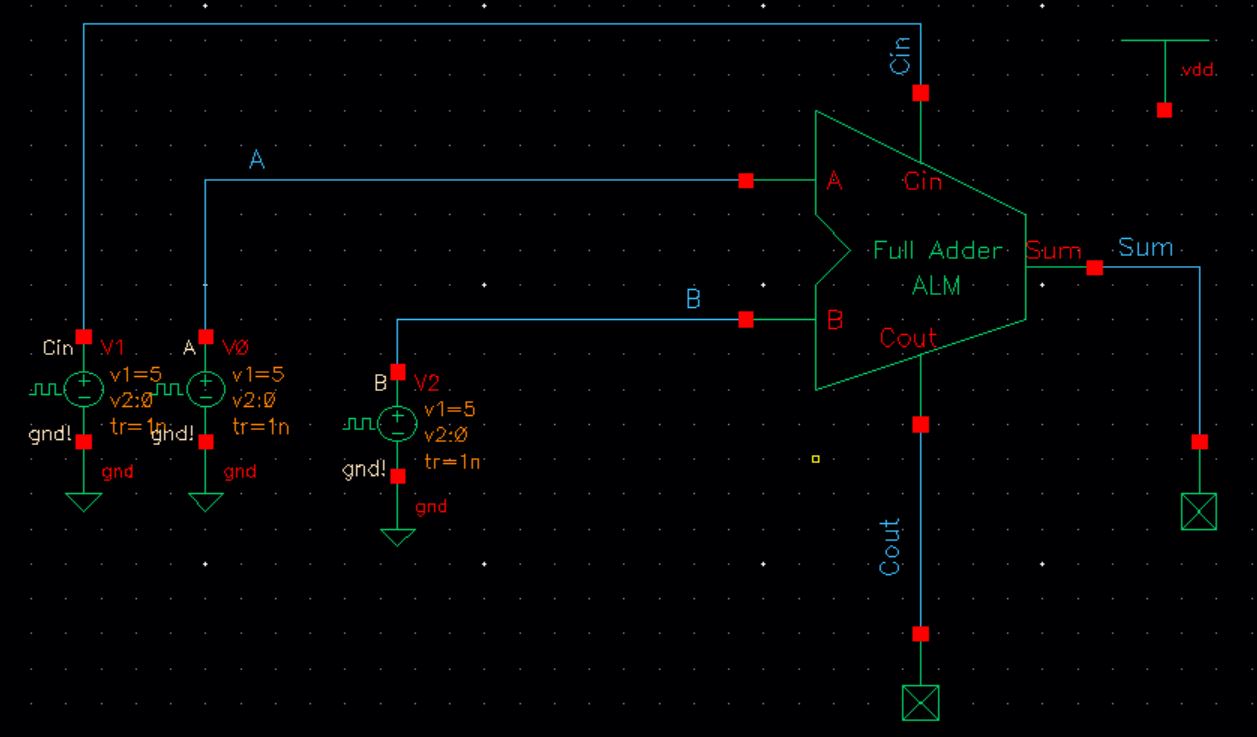
Next
I will design the full adder. This was made easier by using previous
layouts as instances. The tricky part for the full adder was wiring the
layout.
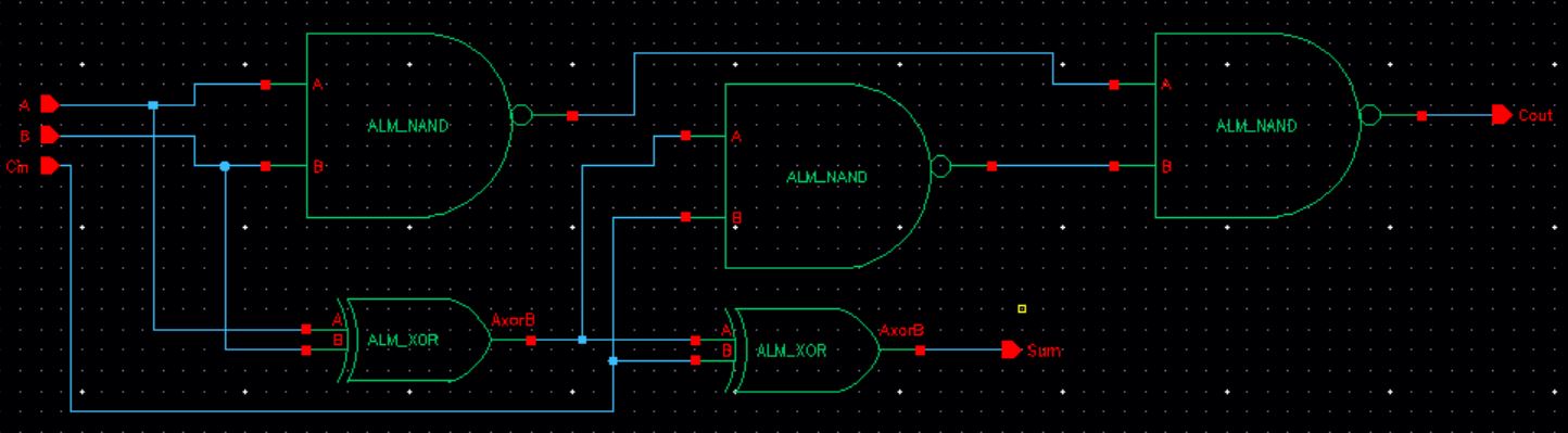
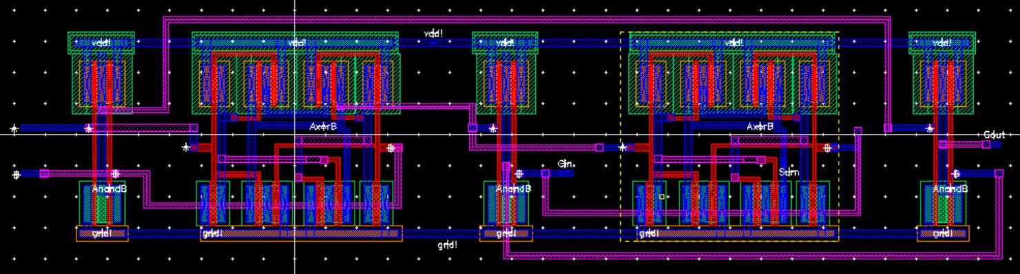
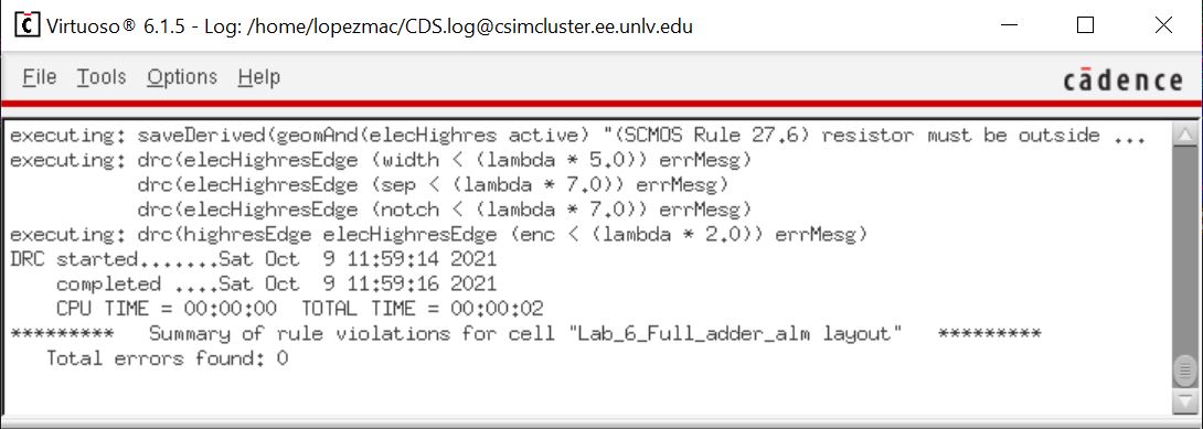
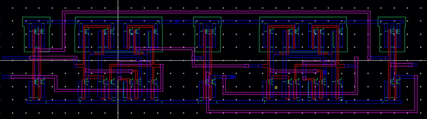
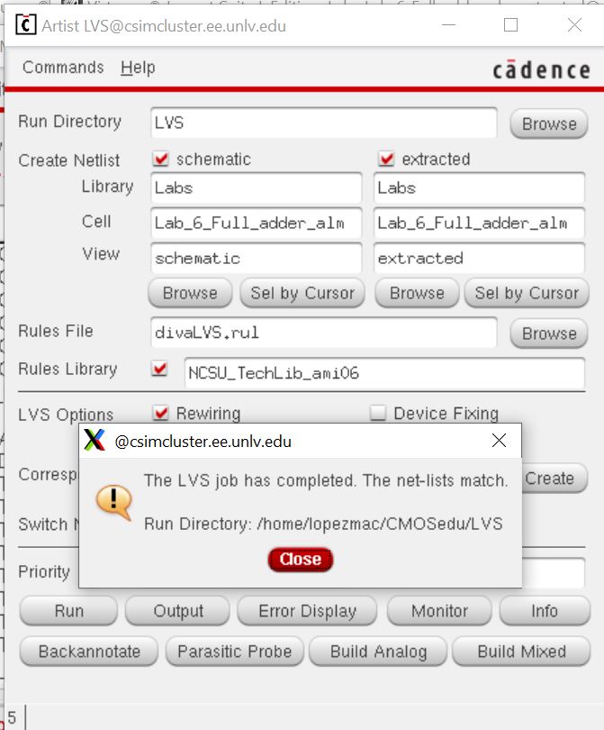
Next I will show the Layout,DRC,LVS, and extracted view.
Fianlly
I will test the Full-Adder and show the results. Before I show the
results I will provide the truth table for and adder to confirm the
results are correct.
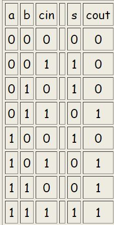
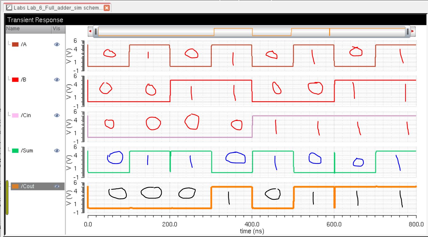
The results match the truth tale. This concludes lab 6.
Backing up work
As always my work was backed up twice.
Return to Labs