Lab 4 - EE 421L
Authored
by Adrian Lopez-Macuaran,
lopezmac@unlv.nevada.edu
September 15, 2021
Lab
description
For this lab we will be covering the characterizations of IV NMOS and PMOS. We will also cover the layout of the NMOS and PMOS.
Pre-Lab
- Back-up all of your work from the lab and the course.
- Read through this lab before starting it.
- Go through Tutorial 2 seen here.
- In
the simulations in this lab the body of all NMOS devices (the
substrate) should be at ground (gnd!) and the body of all PMOS devices
(the n-well) should be at a vdd! of 5V.
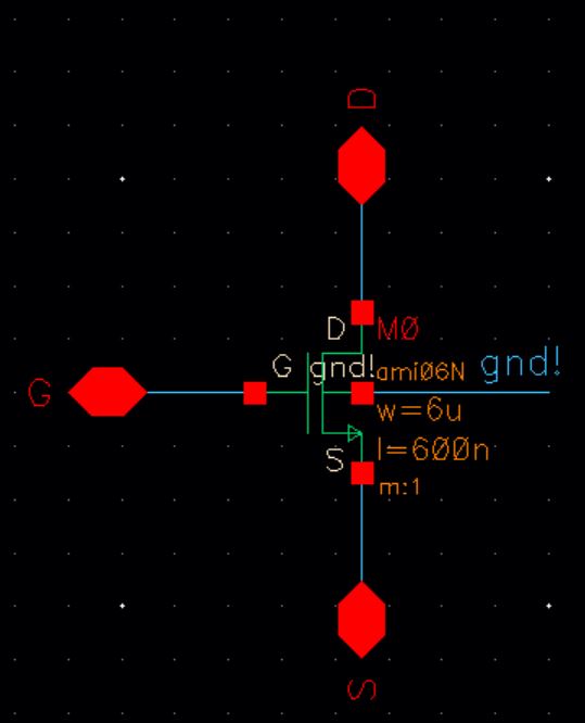
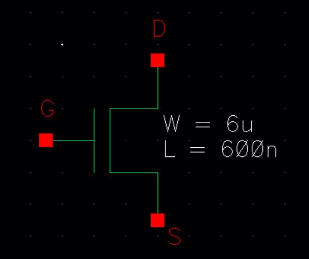
Following
the instruction from Tutorial 2 the first part of the pre-lab was to
make and NMOS schematic then make a symbol from the schematic.
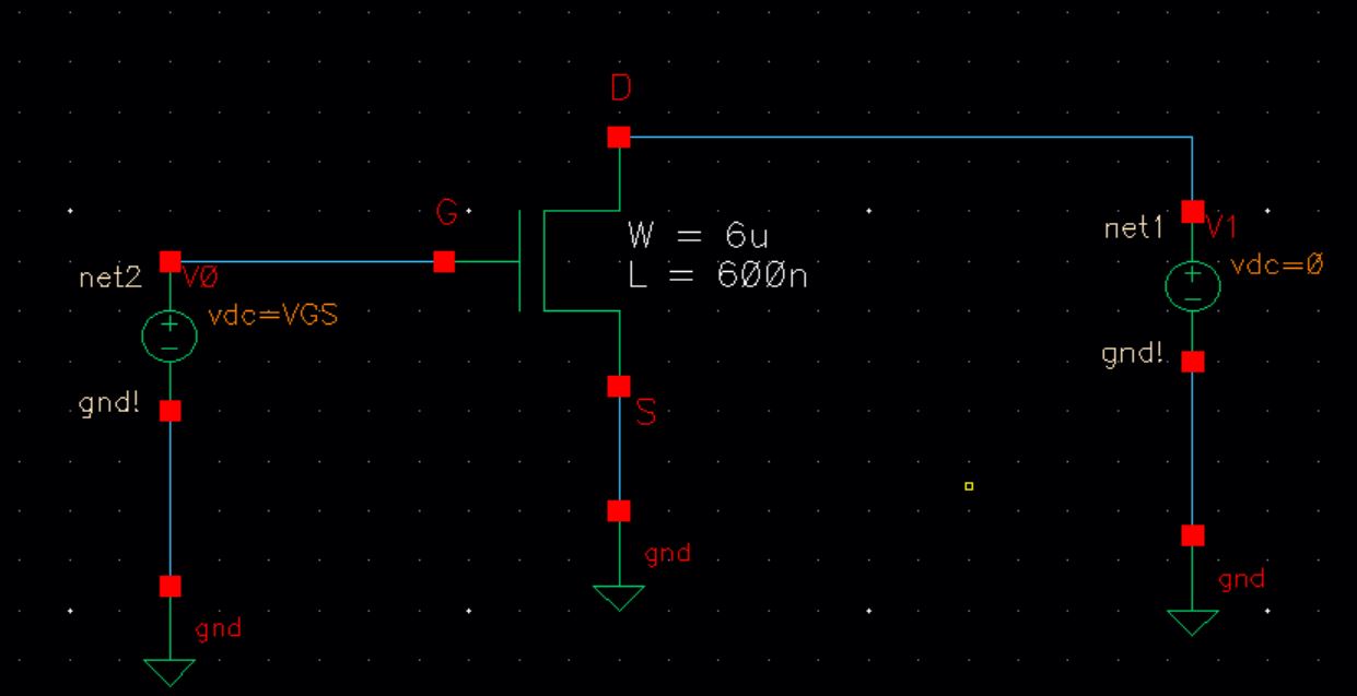
Using
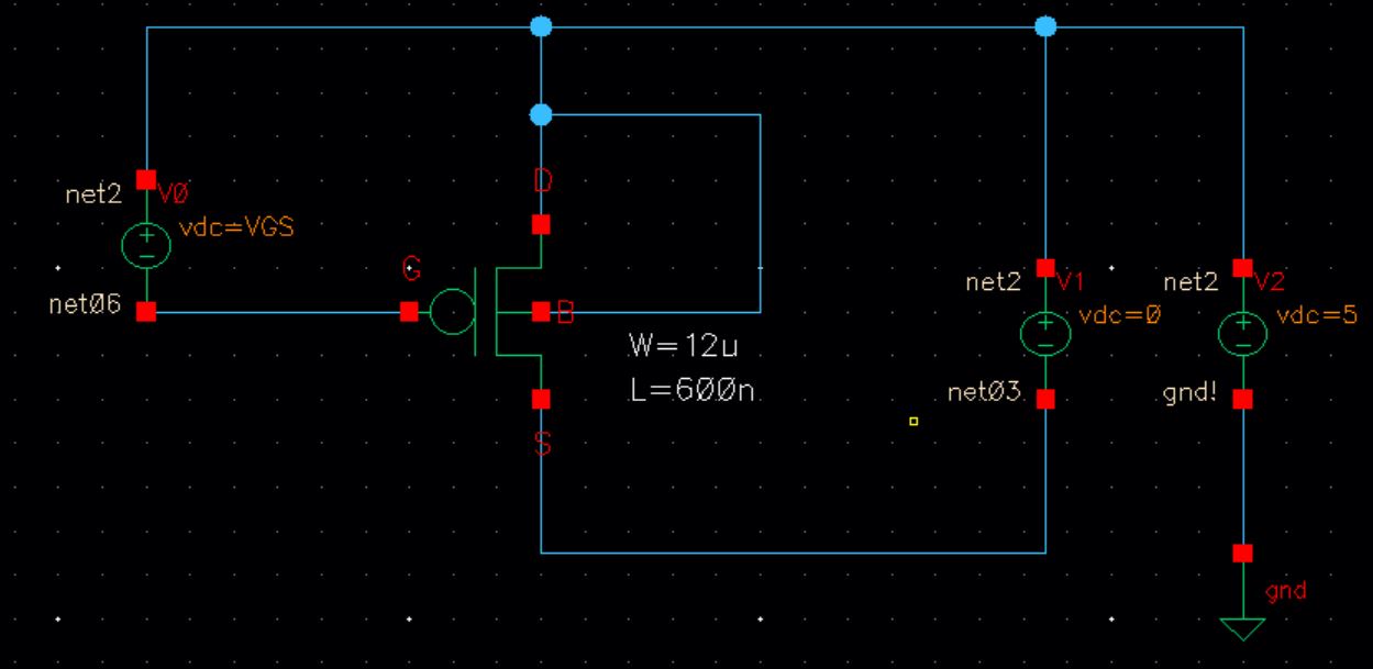
the symbol from above we were to create a circuit to test the NMOS.
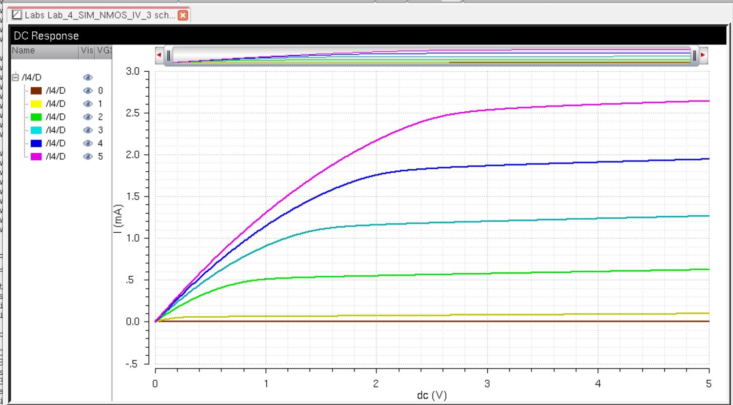
Next we lauched ADE and ran the simulaiton using parametric analysis
showing the NMOS IV curve while varying VGS.
Next we will layout the NMOS extracted it and run and LVS.
The next part was to re-run the simulation, but using the extracted view. This produced the same graph.
Next we will do the same procedure for the PMOS. First the schematic and symbol.
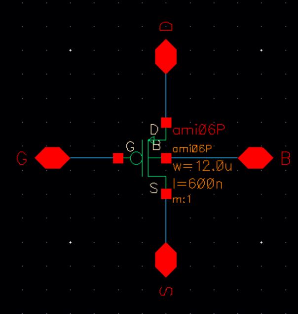
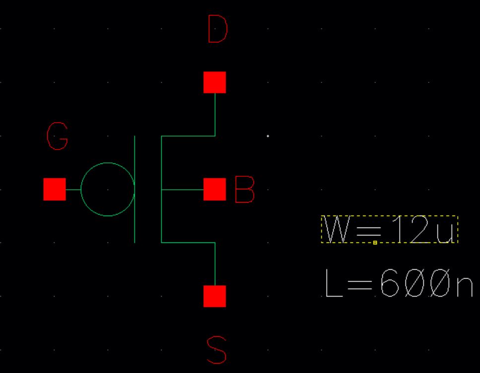
Next we will do creat the schematic followed by the simulation and the graph results.
Next we will layout the PMOS extract it and run a LVS to make sure the net list match.
Now we run the same simulation with the PMOS making sure the EXTRACTED is placed before the simulation.
This works just like our regular simulaiton. This concludes the prelab.
Lab Task:
- Generate 4 schematics and simulations (see the examples in the Ch6_IC61 library, but note that for the PMOS body should be at vdd! instead of gnd!):
- A schematic for simulating ID
v. VDS of an NMOS device for VGS varying from 0 to 5 V in 1 V steps
while VDS varies from 0 to 5 V in 1 mV steps. Use a 6u/600n
width-to-length ratio.
- A
schematic for simulating ID v. VGS of an NMOS device for VDS = 100 mV
where VGS varies from 0 to 2 V in 1 mV steps. Again use a 6u/600n
width-to-length ratio.
- A
schematic for simulating ID v. VSD (note VSD not VDS) of a PMOS device
for VSG (not VGS) varying from 0 to 5 V in 1 V steps while VSD varies
from 0 to 5 V in 1 mV steps. Use a 12u/600n width-to-length ratio.
- A
schematic for simulating ID v. VSG of a PMOS device for VSD = 100 mV
where VSG varies from 0 to 2 V in 1 mV steps. Again, use a 12u/600n
width-to-length ratio.
- Lay
out a 6u/0.6u NMOS device and connect all 4 MOSFET terminals to probe
pads (which can be considerably smaller than bond pads [see MOSIS design rules] and directly adjacent to the MOSFET (so the layout is relative small).
- Show your layout passes DRCs.
- Make a corresponding schematic so you can LVS your layout.
- Lay out a 12u/0.6u PMOS device and connect all 4 MOSFET terminals to probe pads.
- Show your layout passes DRCs.
- Make a corresponding schematic so you can LVS your layout.
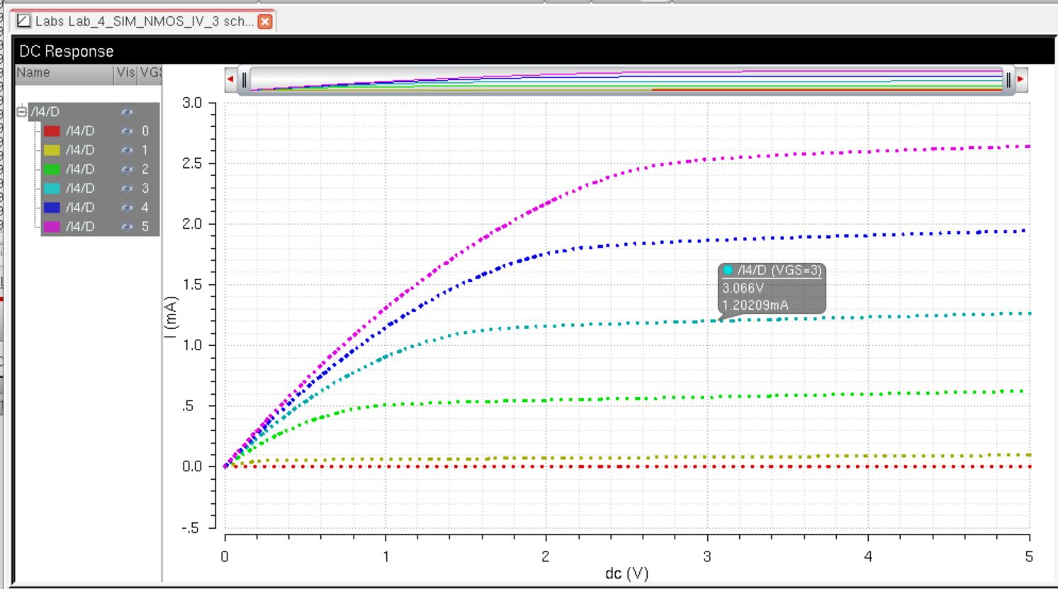
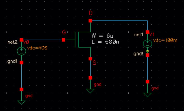
Task 1 is simulating ID
v. VDS of an NMOS device for VGS varying from 0 to 5 V in 1 V steps
while VDS varies from 0 to 5 V in 1 mV steps This is the circuit we did in the prelab so the simulation results are the same.The following will show both schematics and graphs.
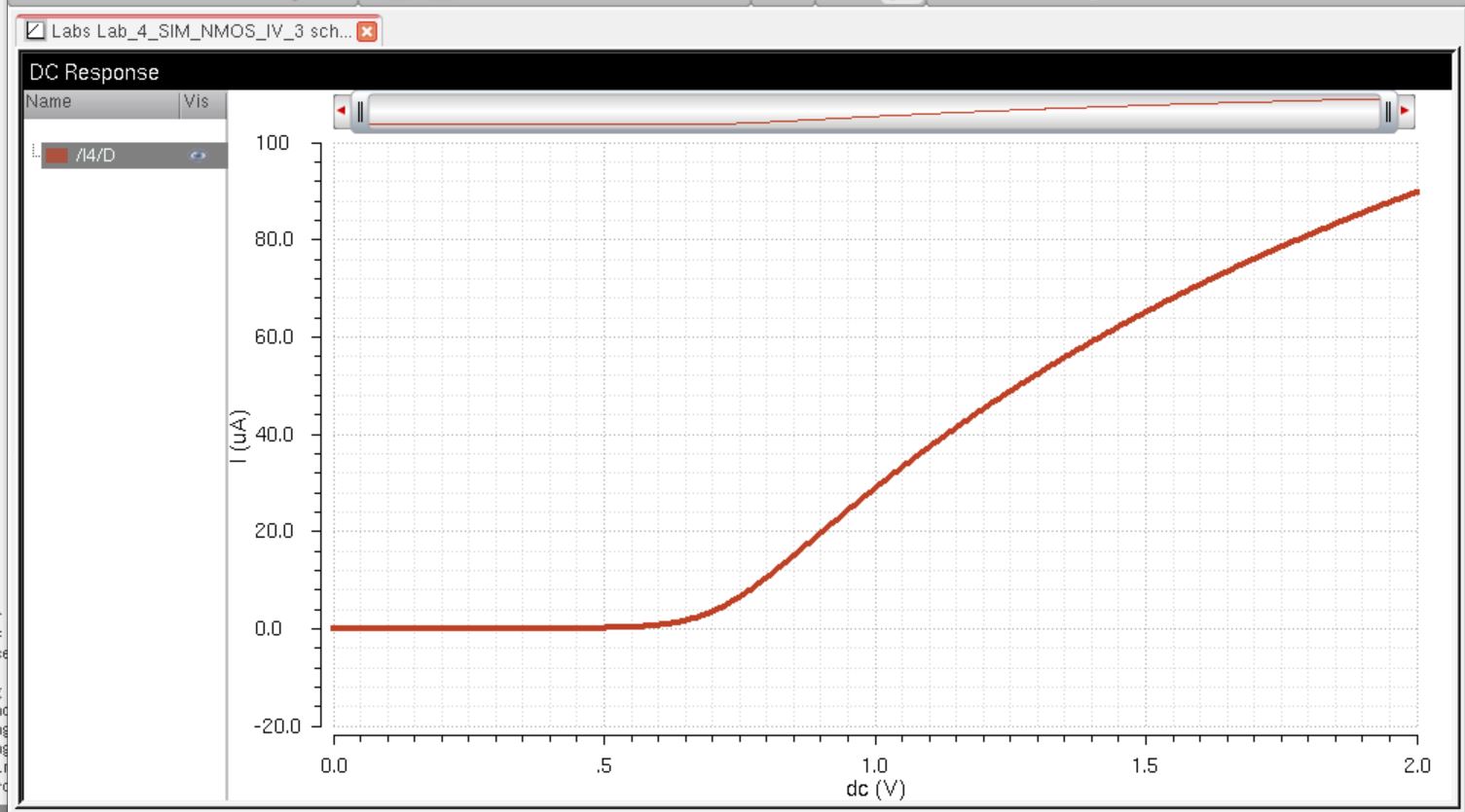
Following ID v. VGS of an NMOS device for VDS = 100 mV
where VGS varies from 0 to 2 V in 1 mV steps.
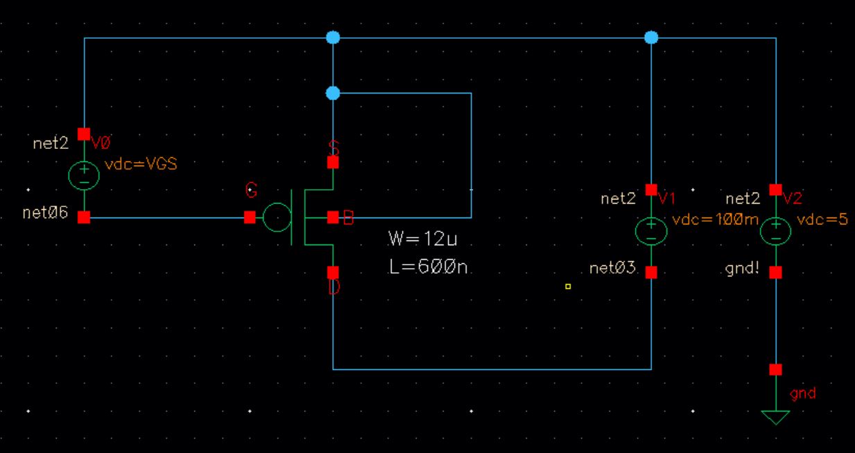
Next task is simulating ID v. VSD (note VSD not VDS) of a PMOS device
for VSG (not VGS) varying from 0 to 5 V in 1 V steps while VSD varies
from 0 to 5 V in 1 mV steps.
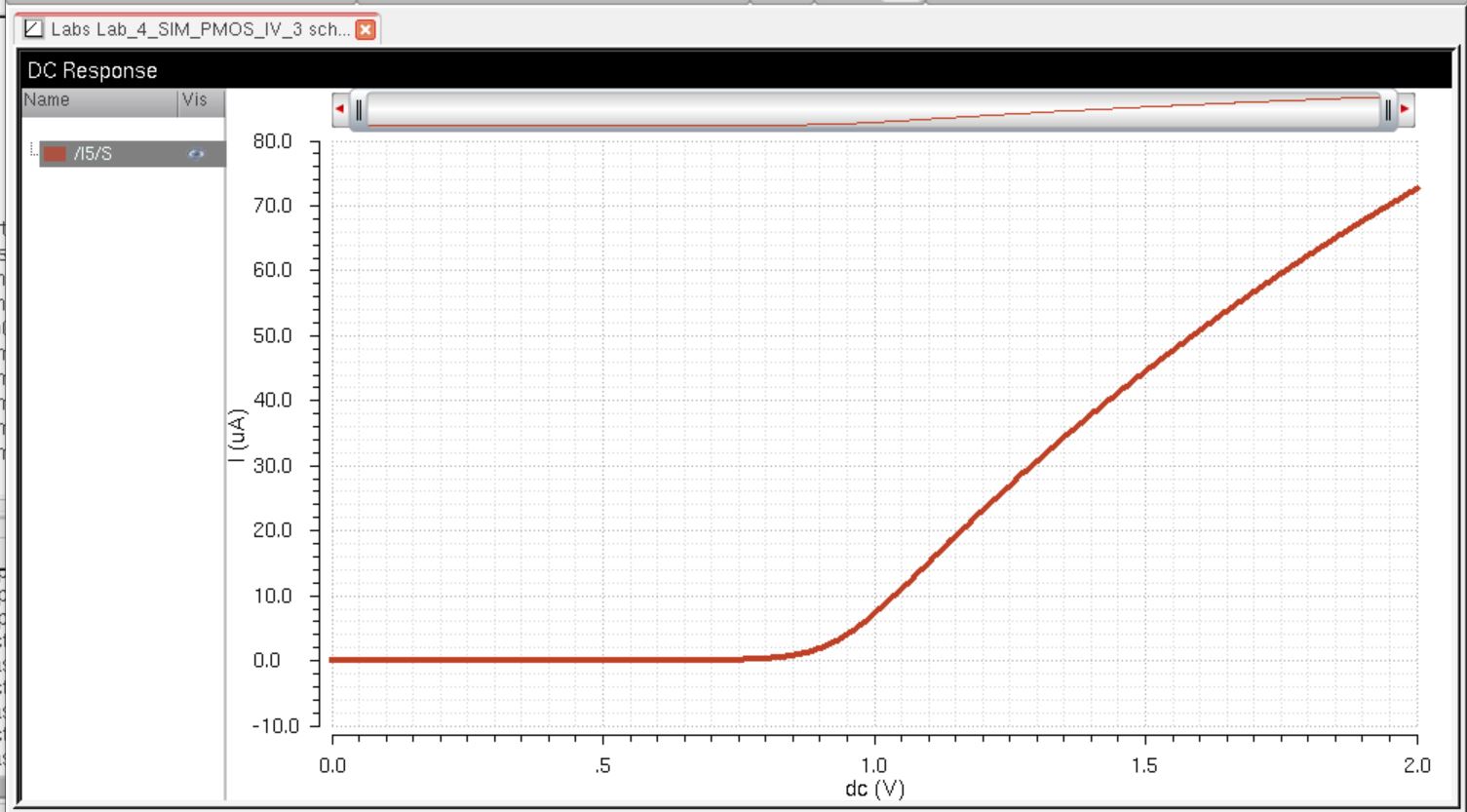
Next simulating ID v. VSG of a PMOS device for VSD = 100 mV
where VSG varies from 0 to 2 V in 1 mV steps. Again, use a 12u/600n
width-to-length ratio.
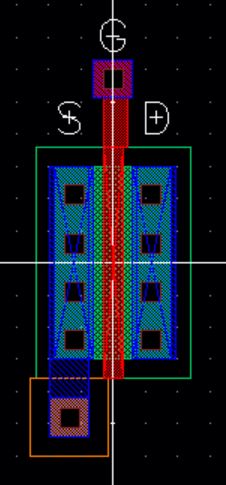
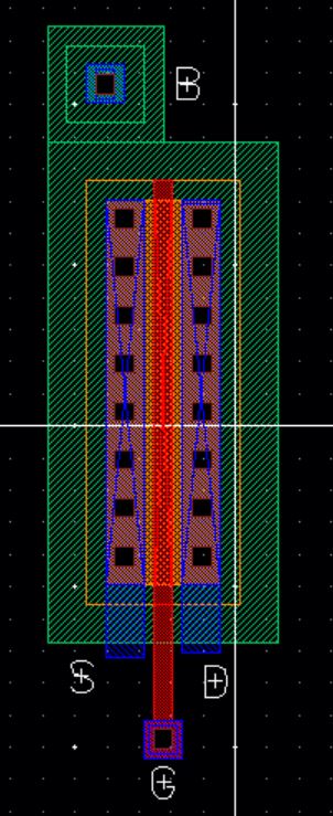
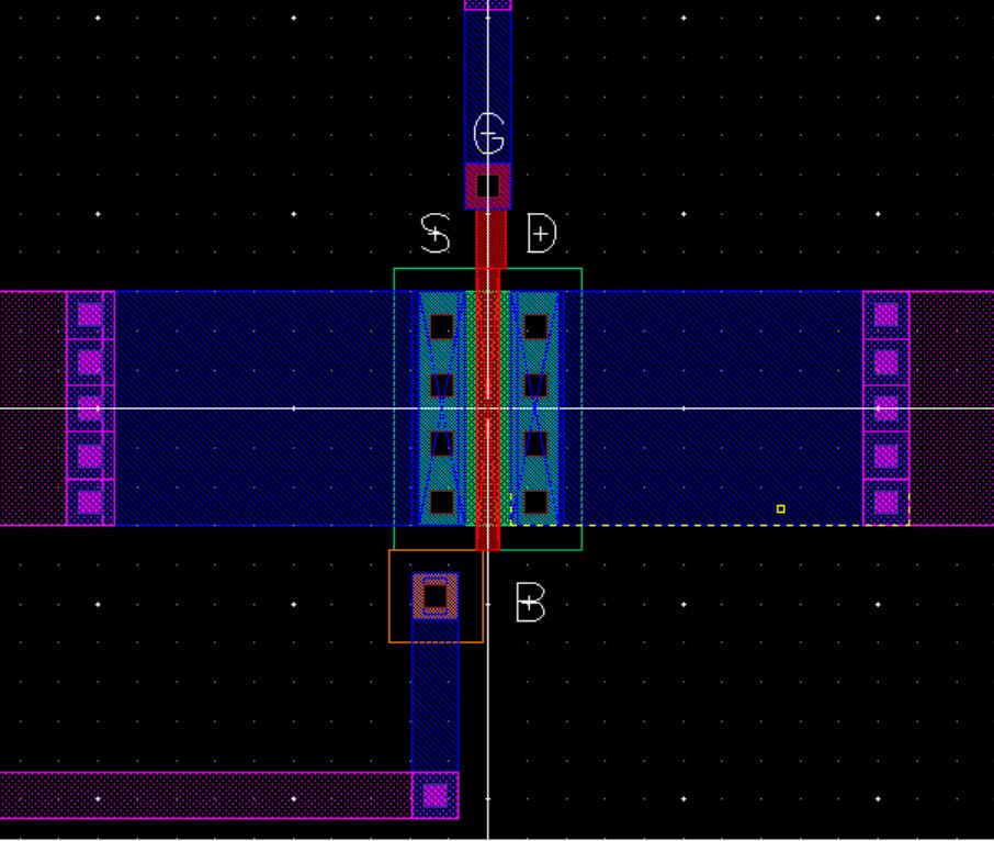
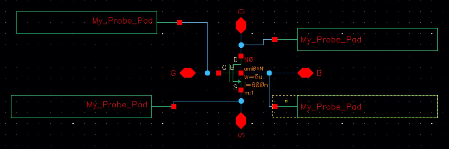
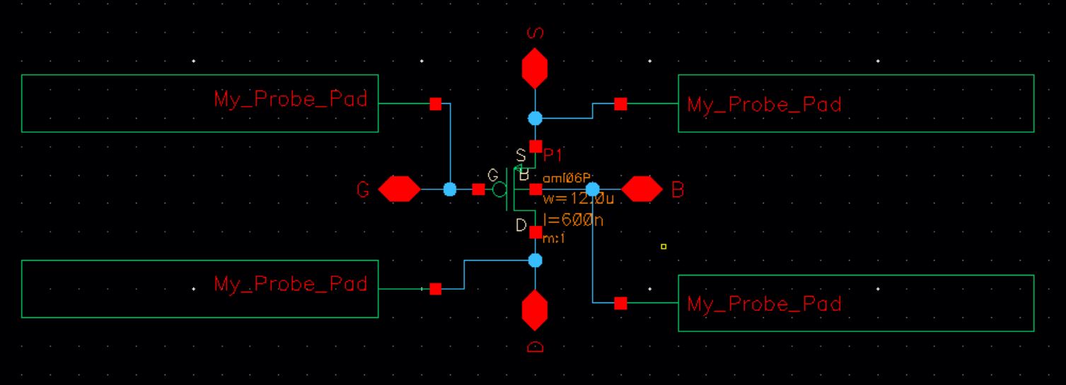
Layout
of 6.0u/o.6u NMOS device with probe pads. The probe pads were made of a
square of 'GLASS' layer, enclosed in a square of 'Metal 3' layer. In
order to connect the probe pads to the NMOS we had to use m1_m2
connectors as well as m2_m3 connectors. The probe pad could also not be
me more than 30um from the NMOS or it would show a spacing error. The
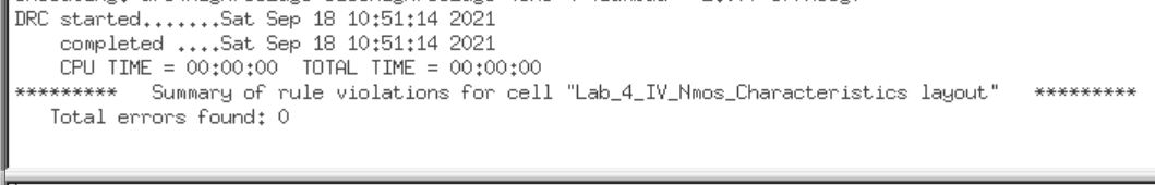
following will show the layout with a passing DRC check.
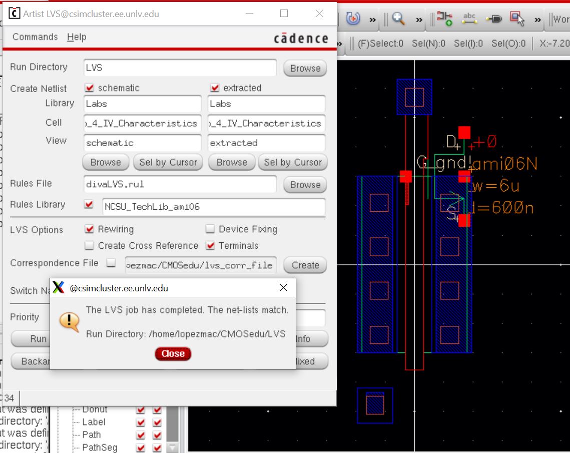
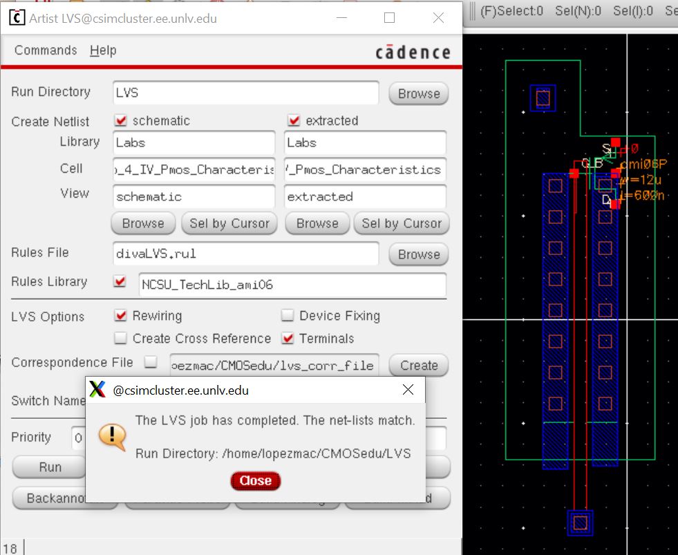
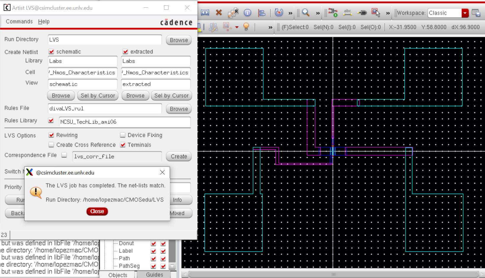
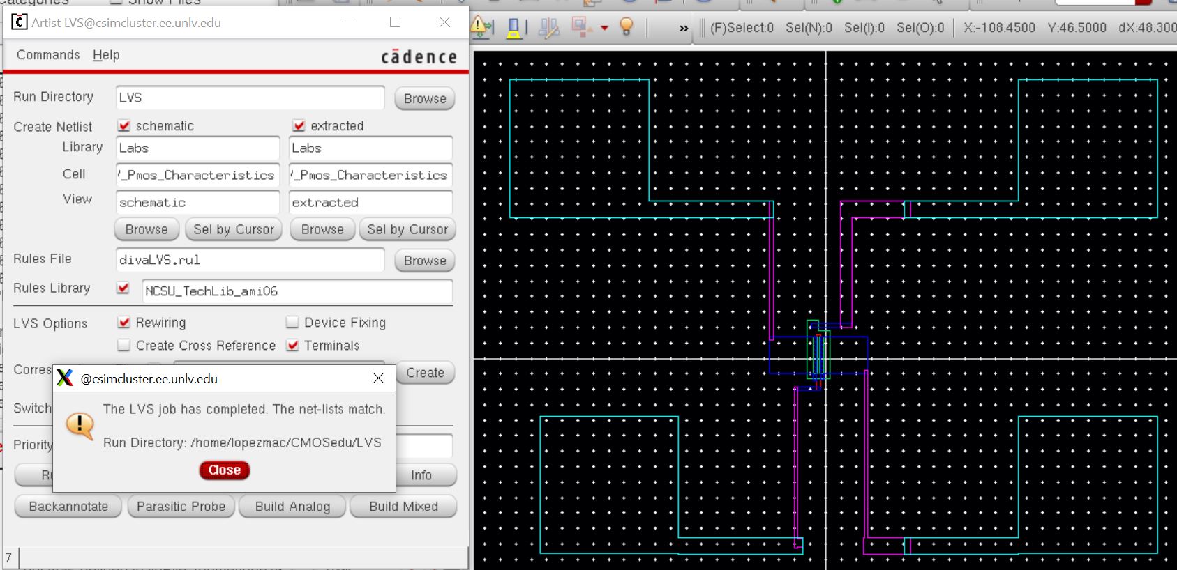
Next
the loyout was extrated. Before running LVS check I had to creat the
porbe pad symbol and new schamtic to match the layout. The following
will show the extracted, schematic, and passing LVS results.
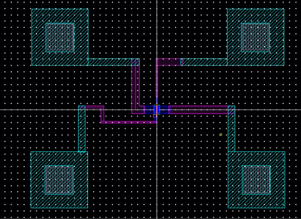
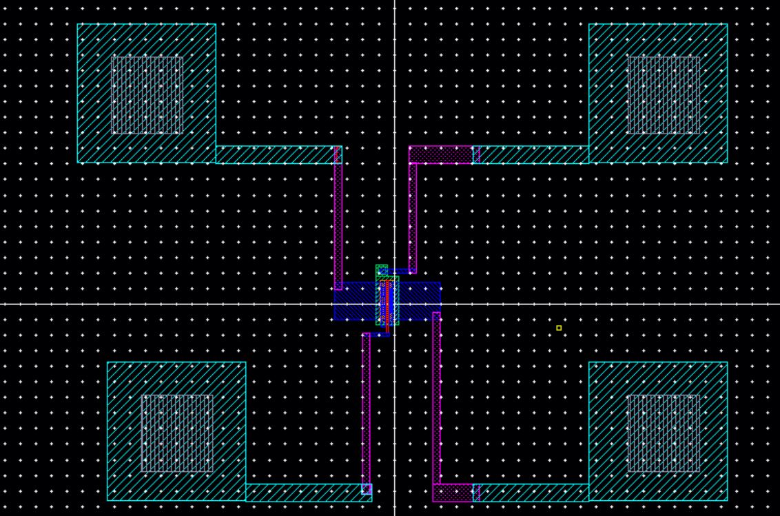
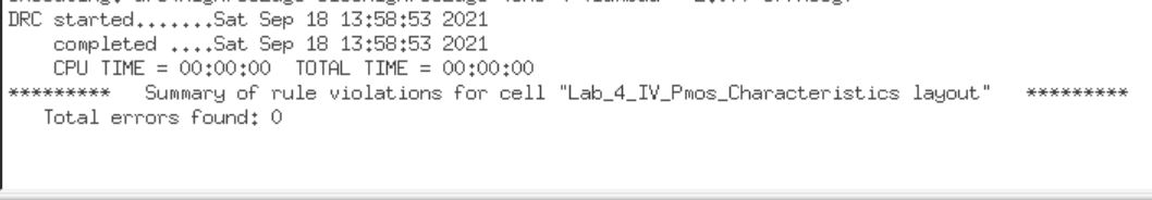
Now we will do the same for a 12u/0.6u PMOS device. The following will show the Layout and DRC with no erros.
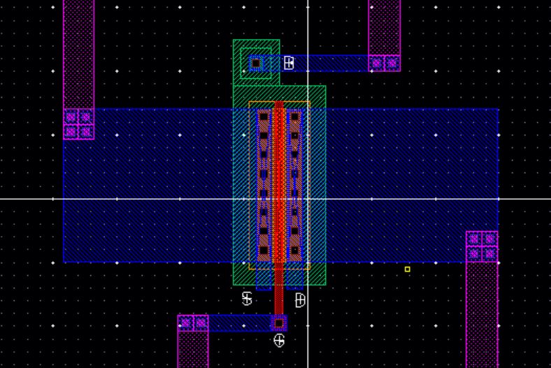
Next Will show the extracted and schamtic for the PMOS with passing LVS results.
This concludes lab 4.
Backing up work
As always I back up my work twice once during the prelab and after the lab is completed.
Return to Labs