Lab 3 - EE 421L
Layout of a 10-bit DAC
ideal circuit. Here, we will make use of the schematic from lab2 and create a layout
that will be used to learn DRC and LVS checking and troubleshooting.
First, to keep things tidy and organized, create a new library "lab3", making sure you copy the tech library used from lab2 library and define the lab3 location in
cds.lib the same way we defined lab2 from the previous report.
Then, since we are building from the resources of lab2, you can also copy the contents of lab2 library into lab3 and edit that way.
Since we are making a 2R_R circuit for the base of our DAC, lets edit the previous
R_R divider into a 2R_R divider: see circuit below:
Using this schematic as our base, lets create a layout under lab3 library.
For the design, follow the intructions on the second half of Tutorial 1
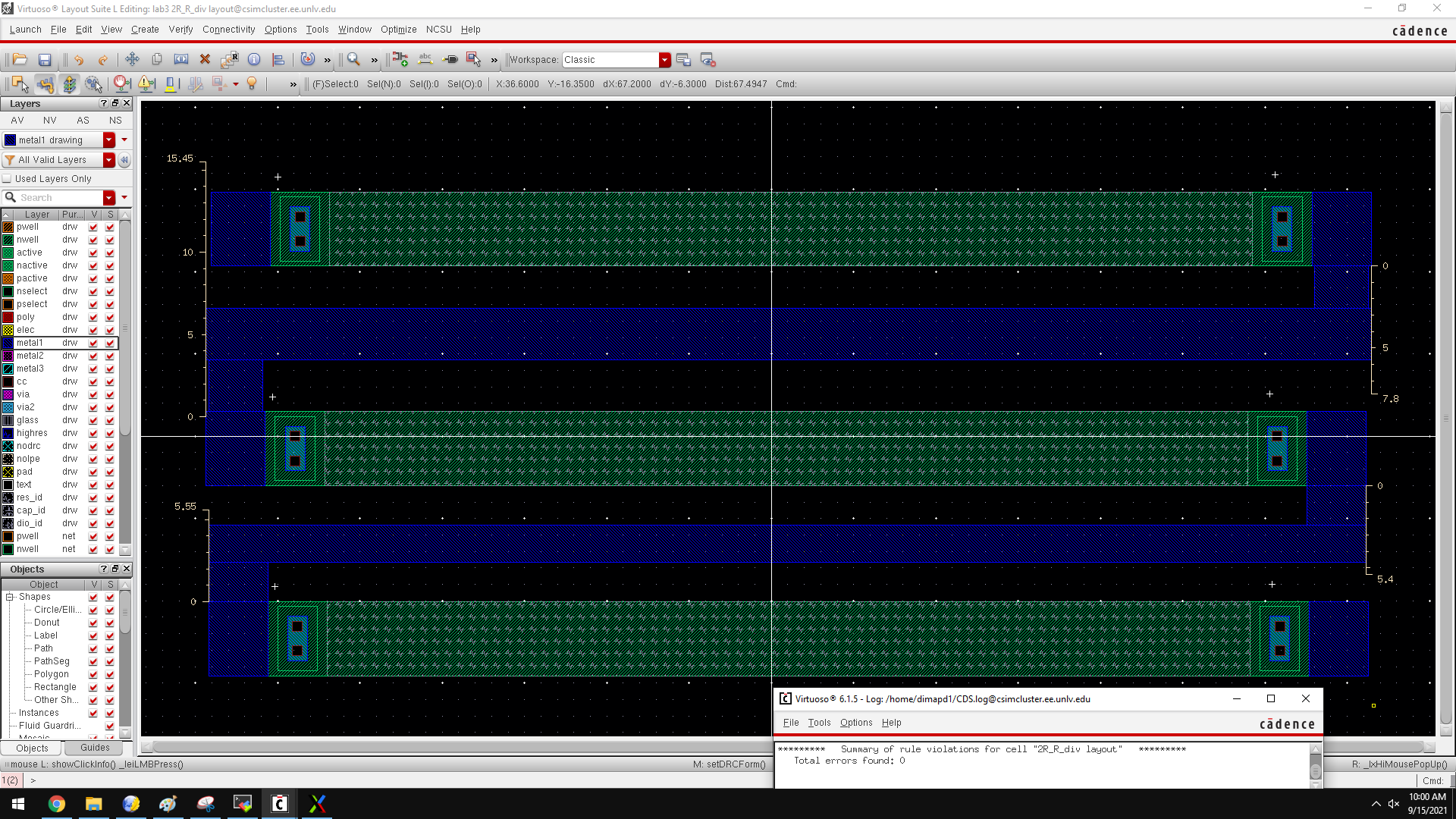
You will end up with a design that looks like this:

Make sure to save and check your progress, then do DRC. If DRC shows no erros,
proceed to LVS to extract another design file.
We will make use of the extraction
as 1 block of 2R_R_div,making 10 copies on a schematic, which will be called B[9:0].
This will then simulate the same way as our custom_DAC.
As per tutorial 1, LVS completes successfuly but with errors. For the design above, I go the following error:
-------------------------------------------------------------------
Probe files from /home/dimapd1/CMOSedu/LVS/schematic
devbad.out:
netbad.out:
N /net7
? Net does not cross-match. It has 2 connections.
N /outhttp://cmosedu.com/jbaker/courses/ee421L/f21/students/dimapd1/lab3/lvs%20success%20but%20net%20mismatch.png
? Net does not cross-match. It has 2 connections.
netbad.out:
N /1
? Net does not cross-match. It has 1 connections.
N /4
? Net does not cross-match. It has 1 connections.
N /3
? Net does not cross-match. It has 1 connections.
N /2
? Net does not cross-match. It has 1 connections.
---------------------------------------------------------------------
The error indicates a mismatch on the pin names or the names of the node connections between the layout and the schematic. We will have to find the connnections and match the names.