Lab 8 - EE 421L Digital Integrated Circuit Design
The Team
Damian Aceves Franco,
Email: acevesfr@unlv.nevada.edu
David Pinales
Email: pinales@unlv.nevada.edu
Ryan Eclarinal
Email: eclarina@unlv.nevada.edu
Due December 1
********************************************************************
Generating a test chip layout for submission to MOSIS for fabrication
Pre-lab work
- Back-up all of your work from the lab and the course.
- Go through Cadence Tutorial 6 seen here.
- Read through the lab in its entirety before starting to work on it
********************************************************************
PRE-LAB
The pad layer was used by MOSIS to indicate the location of the pads
120 um square centered upon the origin
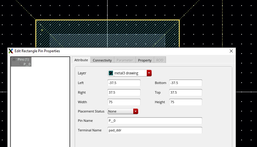
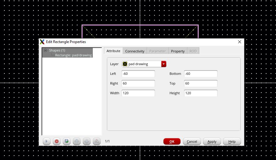
75 um square with overglass
Next instantiate a pin called “pad” with a direction inputOutput

Add a pin on the metal3 layer called pin<1> with a direction of inputOutput

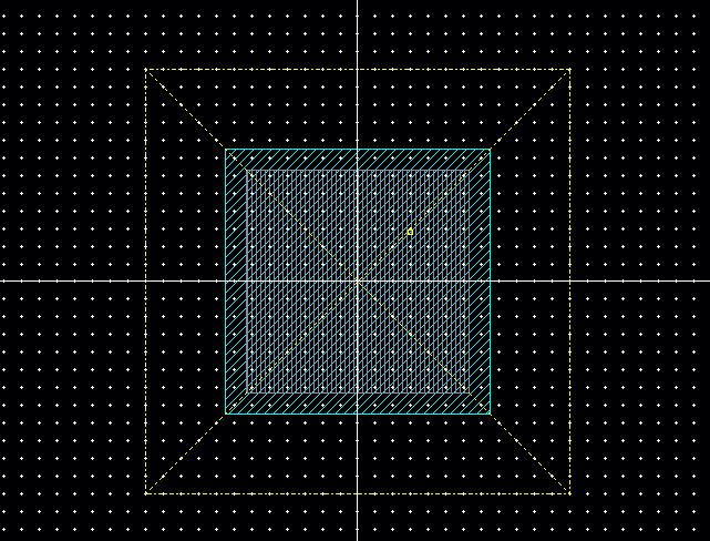
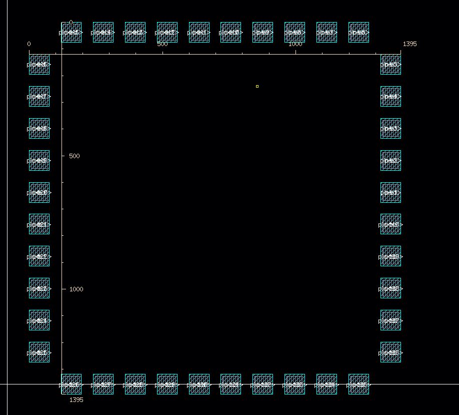
Next copy, c, the pad cell and pin then use F3 and set the number of rows and columns to 12
click in the lower right corner of the first copied cell. Delete the middle, corner, and extra pads/pins to get the basic padframe
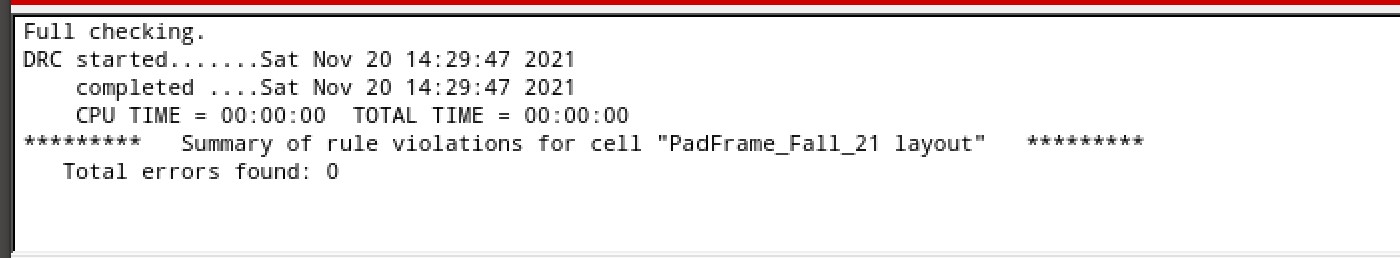
DRC and save the layout
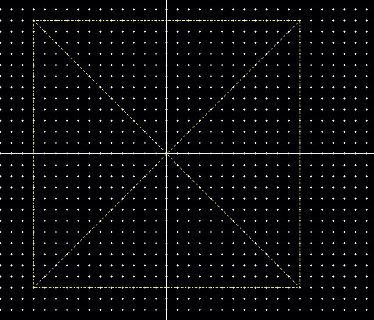
Let’s measure the size of the padframe
Using the ruler we get the following sizes (1.395 mm square)
Generate a schematic cell view for the pad cell and add a pin, called pad, with a direction of inputOutput
Check and Save the schematic.
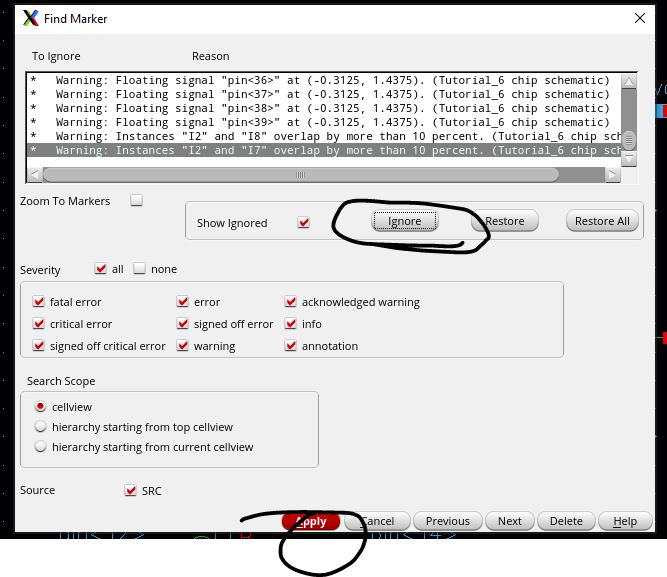
Use Check -> find marker to ignore the warning that the pin is floating.
Check and Save the schematic again

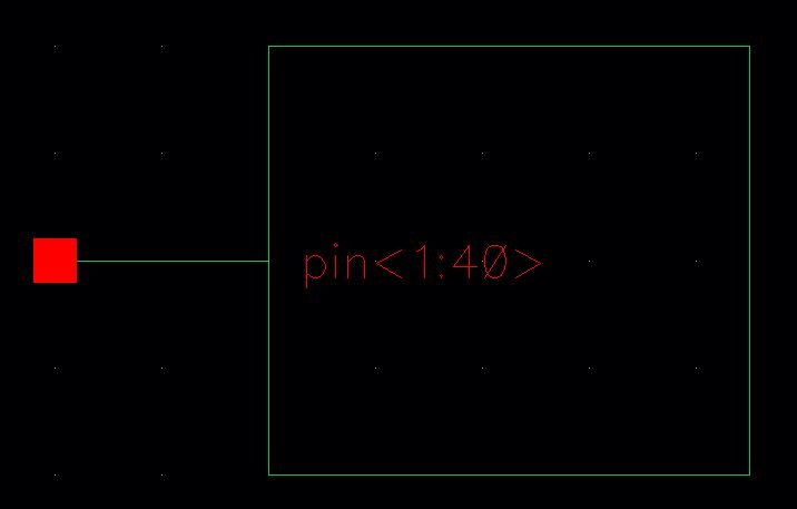
Next use Create -> Cellview -> From Cellview to create a symbol for the pad

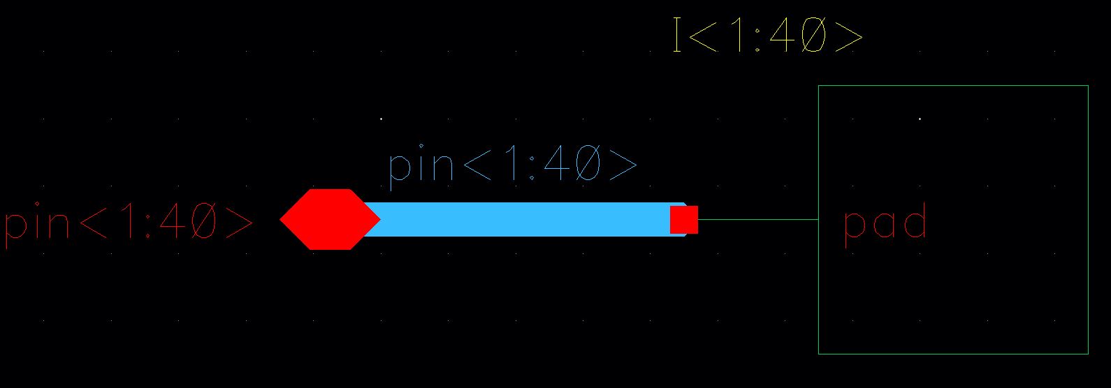
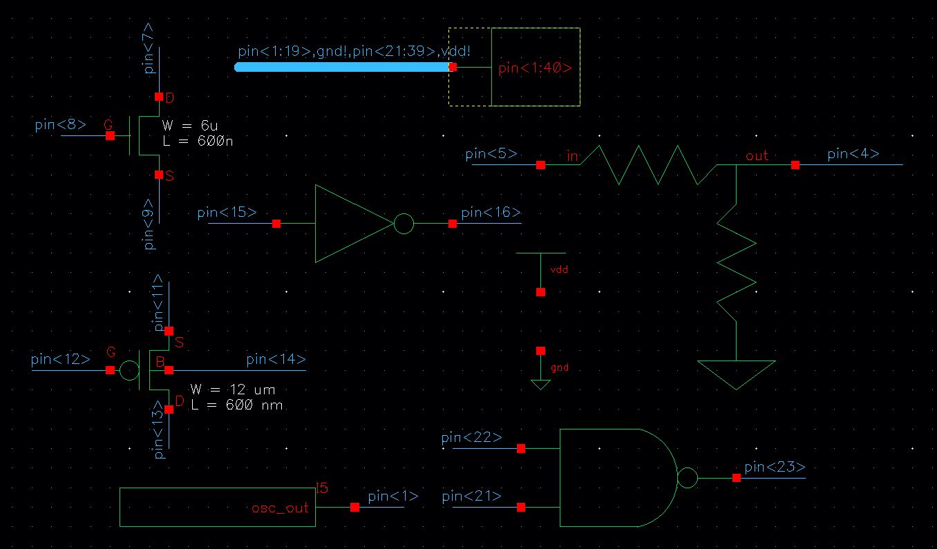
Create a schematic cellview for the padframe and instantiate the pad cell.
Array the instance name and ensure the Display is set to value as seen below
Add a pin with a name of pin<1:40> Add a wide wire with a label pin<1:40>
Check and Save
recreate a symbol for the padframe using Create -> Cellview -> From Cellview
Create a schematic view of a cell called “chip” and add the cells we’ve created in the tutorial.
Wire the cells up as seen (an arbitrary connection).
Note how we’ve used pin<20> for ground and pin<40> for power.
Check and Save
Ignore these warnings and then Check and Save again
We are ready to connect the cells up to the padframe in the layout.
Create of layout view of the “chip” cell.
Place the R_div, NMOS_IV, PMOS_IV, inverter, nand2, and ring oscillator cells near the pads that they will connect to
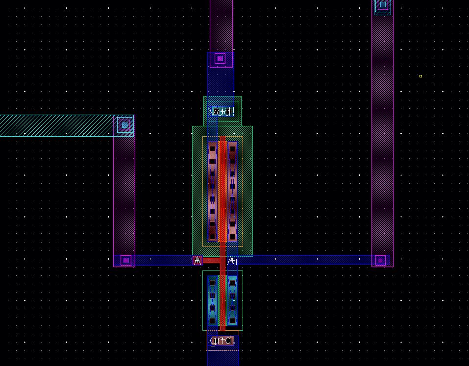
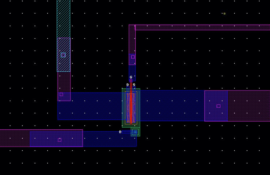
When done setting up and wiring DRC
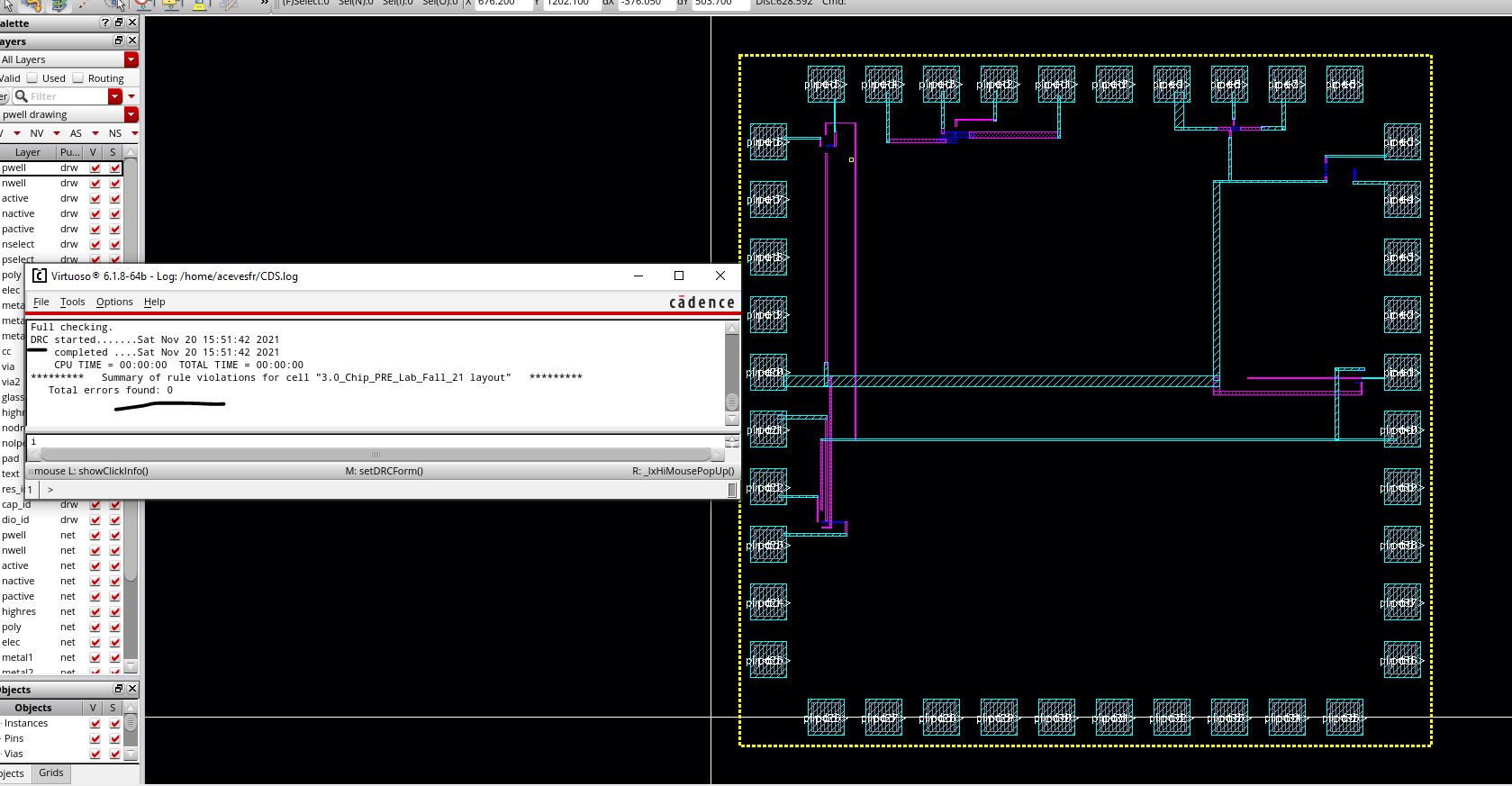
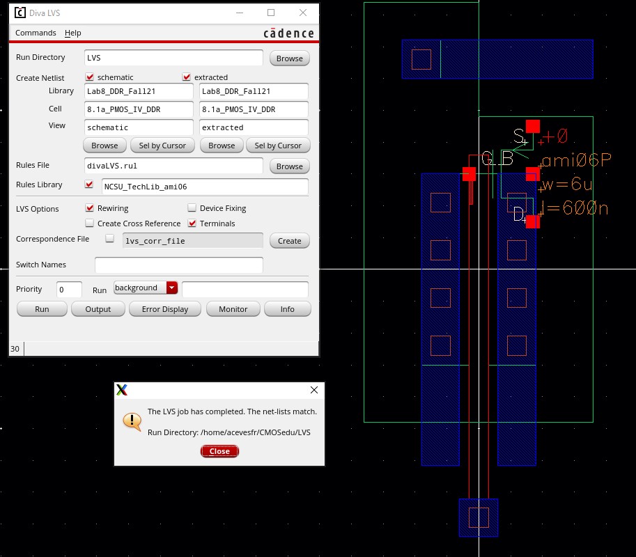
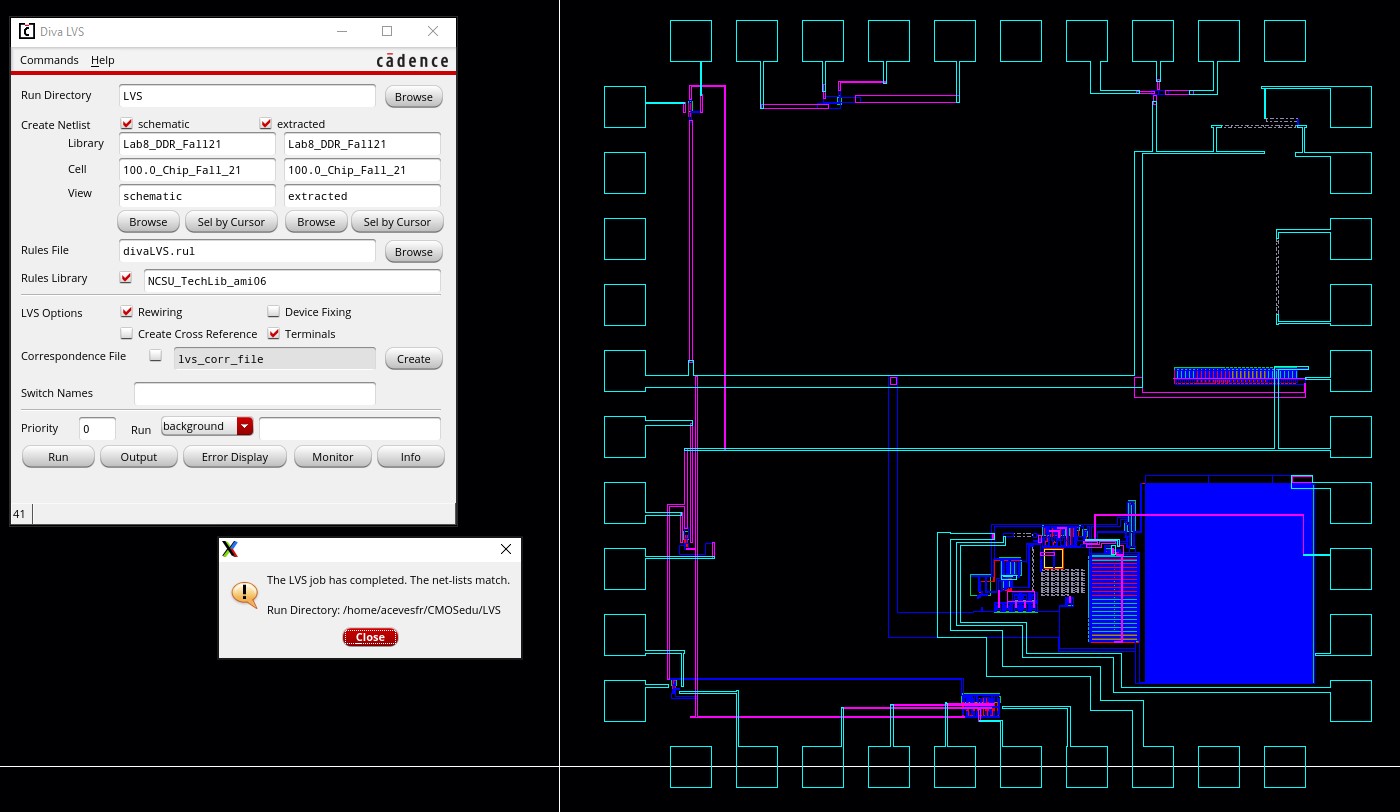
extract the layout and LVS
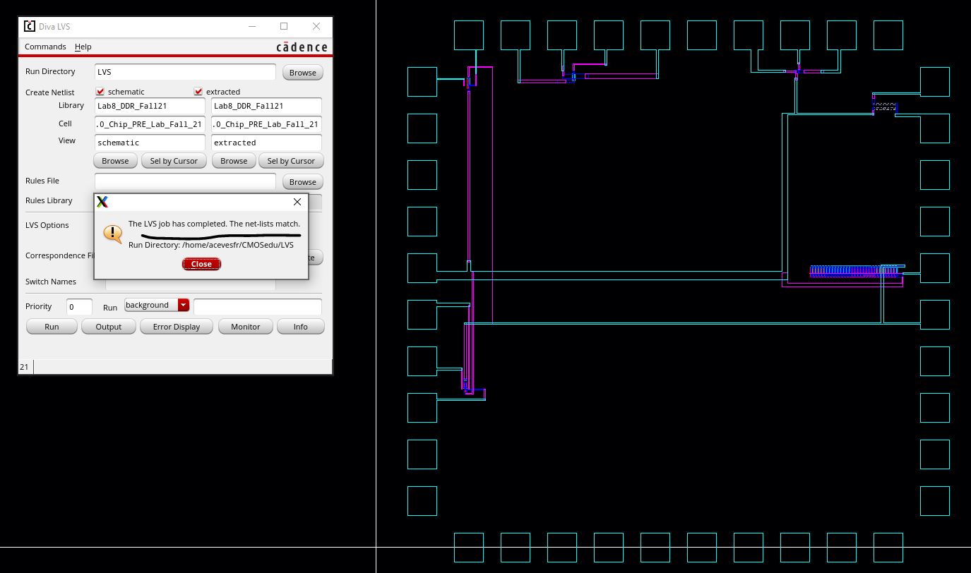
LVS result 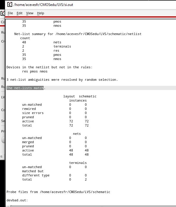
END of PreLab
********************************************************************
Lab
description
The chip should include the following test structures:
- One, or more if possible, course projects
- A 31-stage ring oscillator with a buffer for driving a 20 pF off-chip load
- NAND and NOR gates using 6/0.6 NMOSs and PMOSs
- An inverter made with a 6/0.6 NMOS and a 12/0.6 PMOS
- Transistors,
both PMOS and NMOS, measuring 6u/0.6u where all 4 terminals of each
device are connected to bond pads (7 pads + common gnd pad)
- Note
that only one pad is needed for the common gnd pad. This pad is used to
ground the p-substrate and provide ground to each test circuit
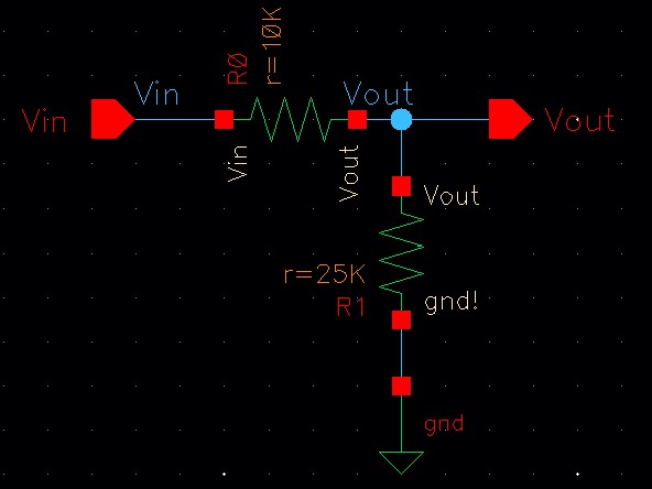
- Using
the 25k resistor laid out below and a 10k resistor implement a voltage
divider (need only 1 more pad above the ones used for the 25k
resistor)
- A 25k resistor implemented using the n-well (connect between 2 pads but we also need a common gnd pad)
- Ground should be pin 20.
Power should not be shared between the circuits so that a vdd!-gnd! short in one circuit doesn't make one of the other circuits inoperable.
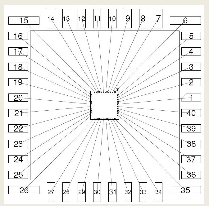
The image
seen at the bottom of the page shows how the chip's pads correspond to
the pins of the 40 pin DIP package we'll receive from MOSIS.
********************************************************************
LAB
One, or more if possible, course projects
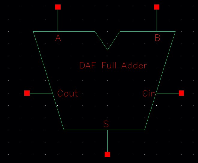
Full Adder
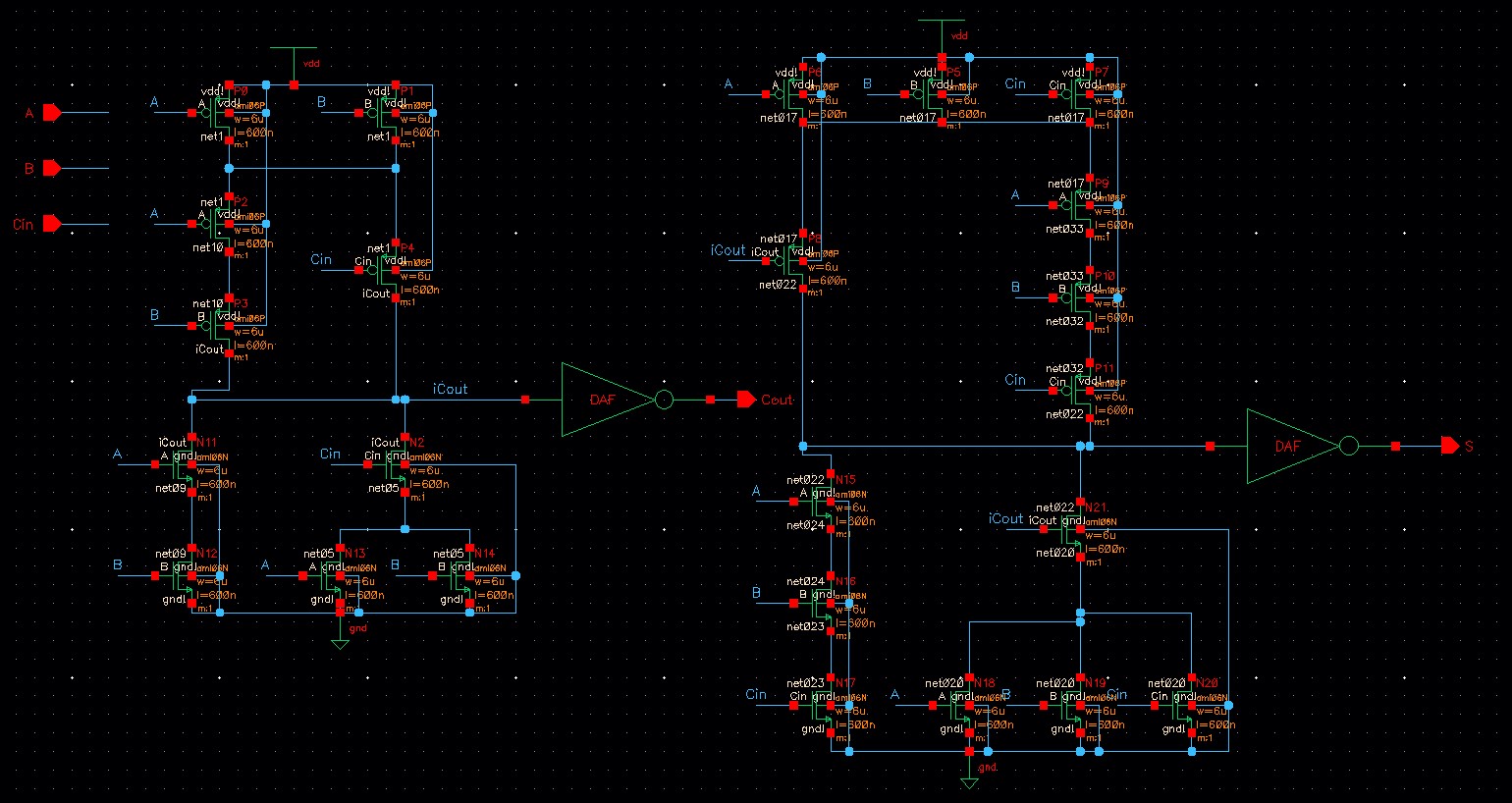
Symbol
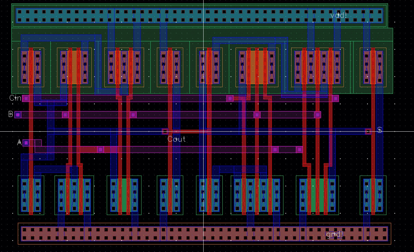
Layout
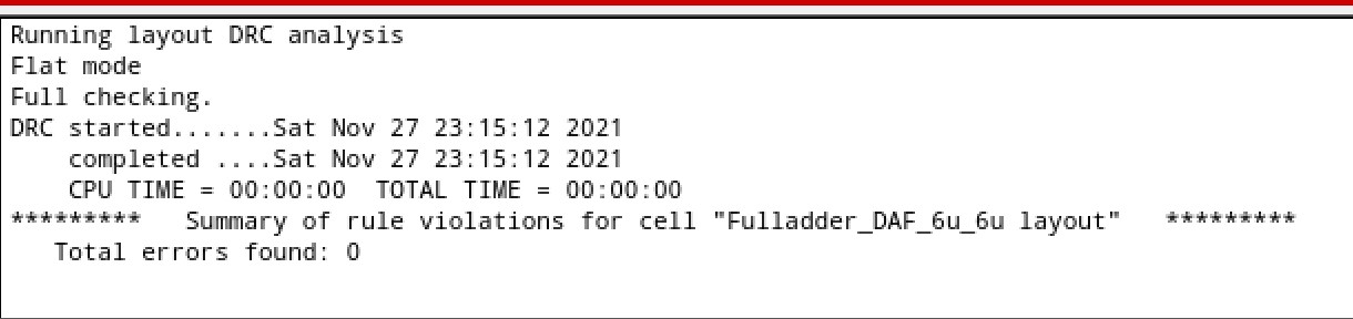
DRC
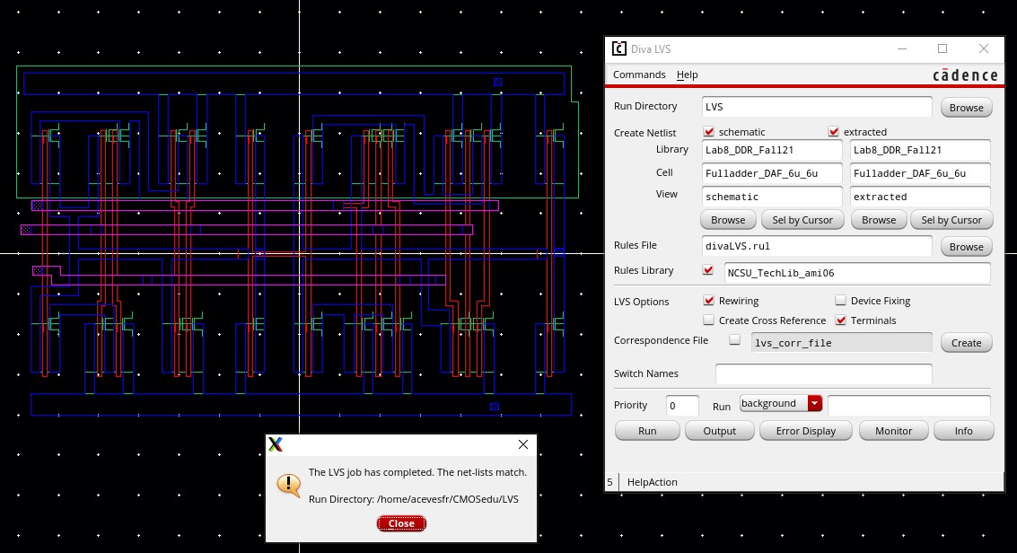
LVS and excract
how to test
pin 28 is input A, pin 29 is input B, pin 30 is Cin input, pin 31 is Cout, and pin 32 is S output
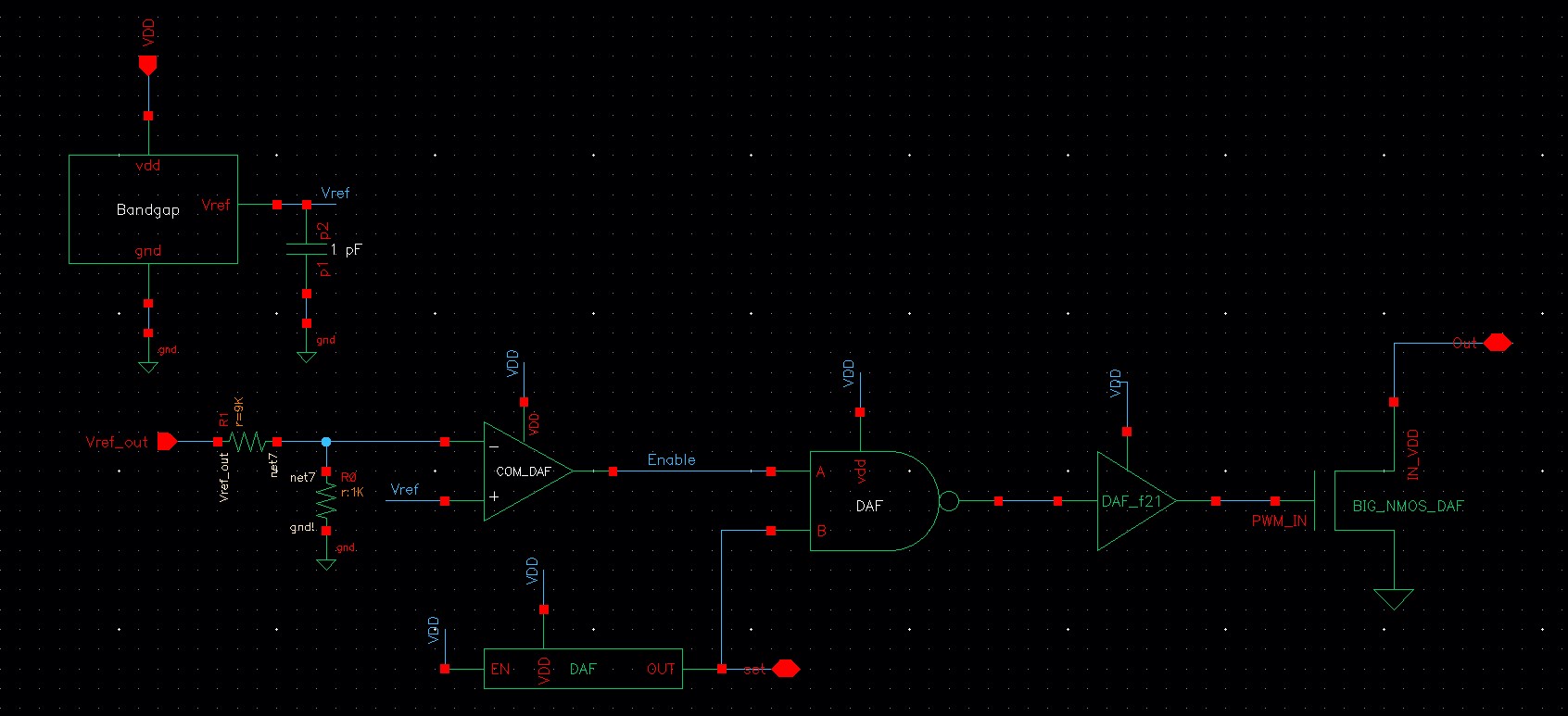
Boost Converter Lecture Project
In 4V to 5.25V, Out 12.5V
Schematic
Layout
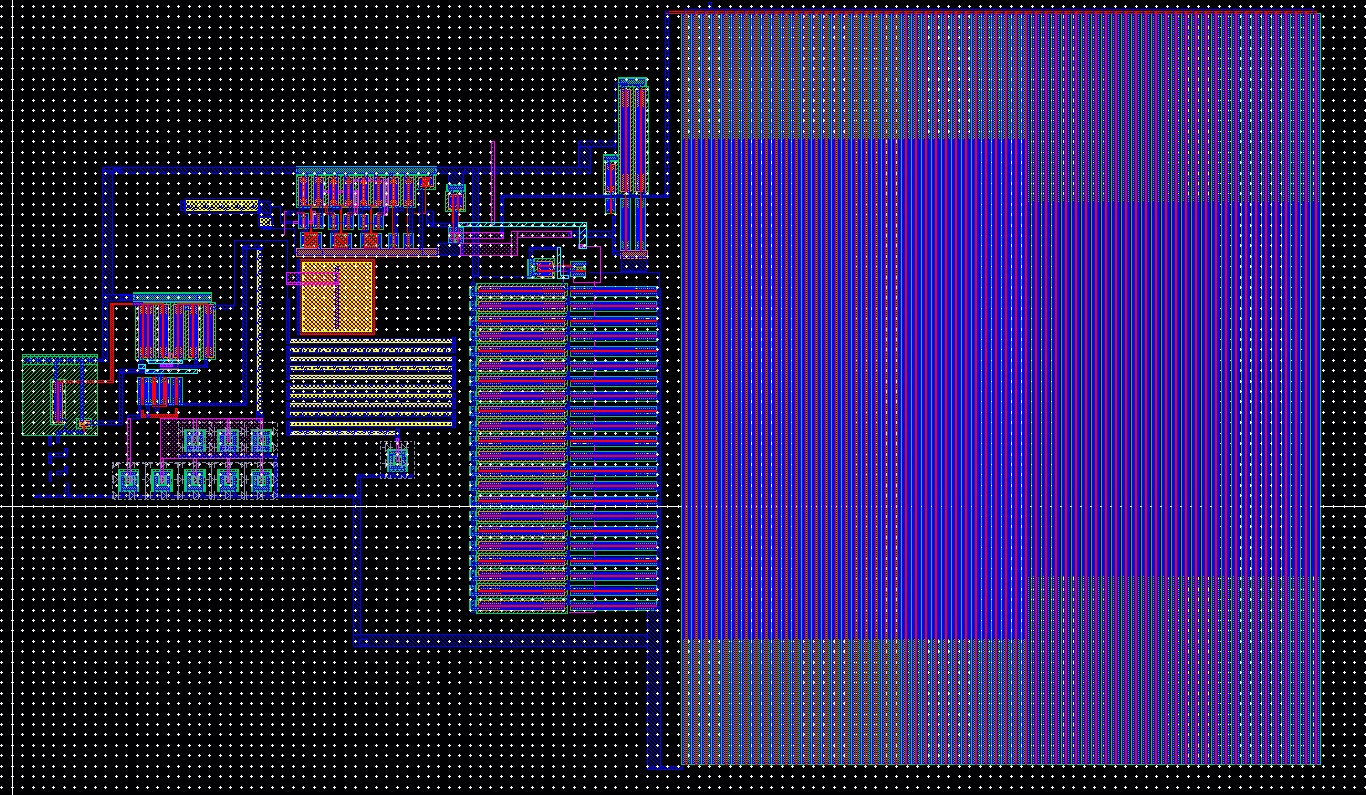
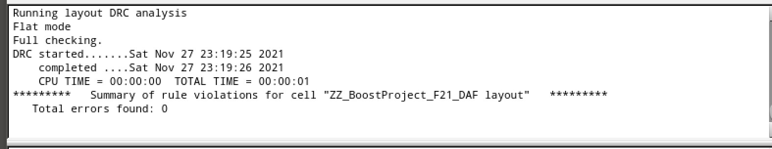
DRC
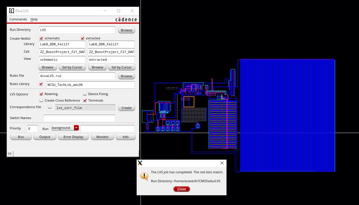
LVS
how to test
pin 38 is the set pin to the boost converter, pin 36 is input Vref, pin 33 is VDD, and pin 39 is Out
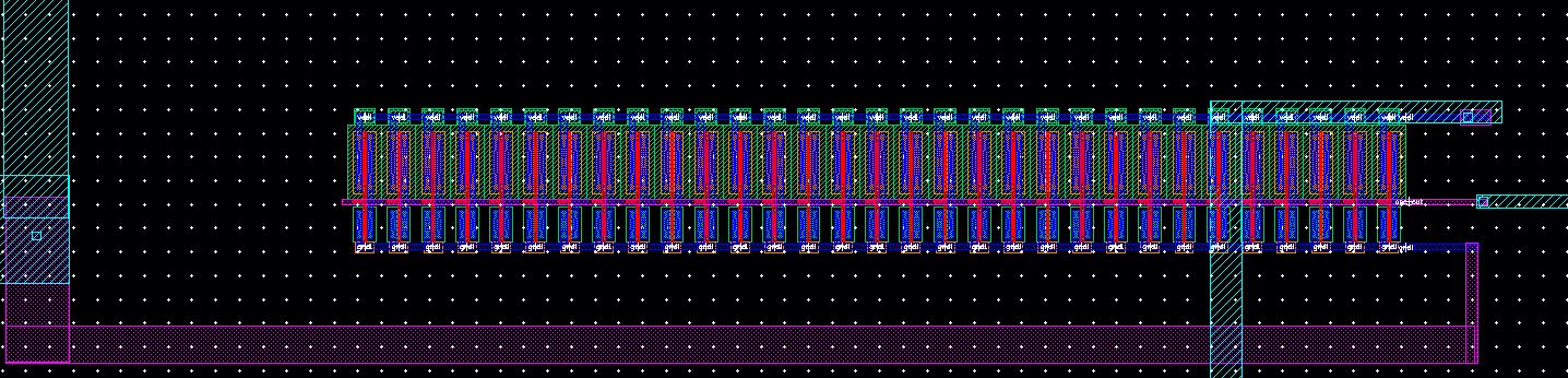
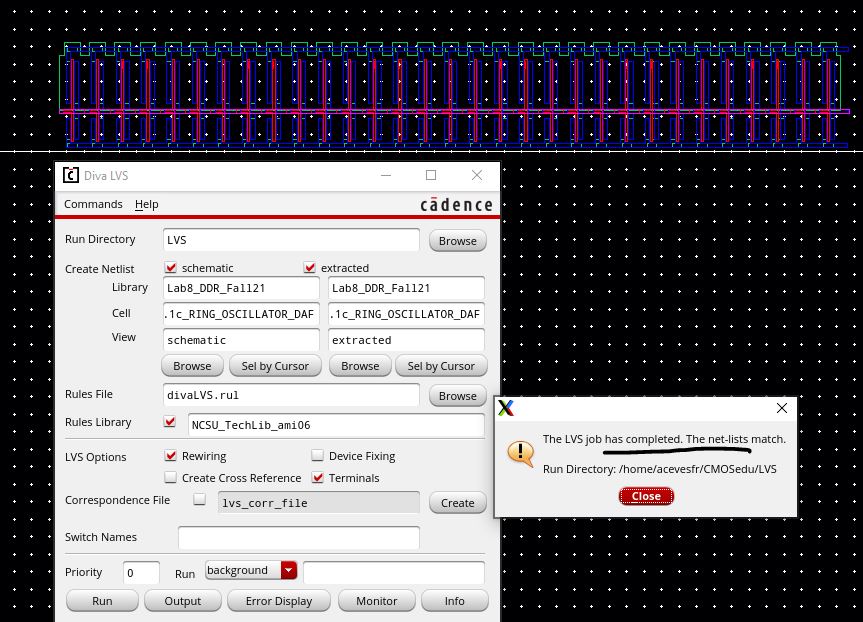
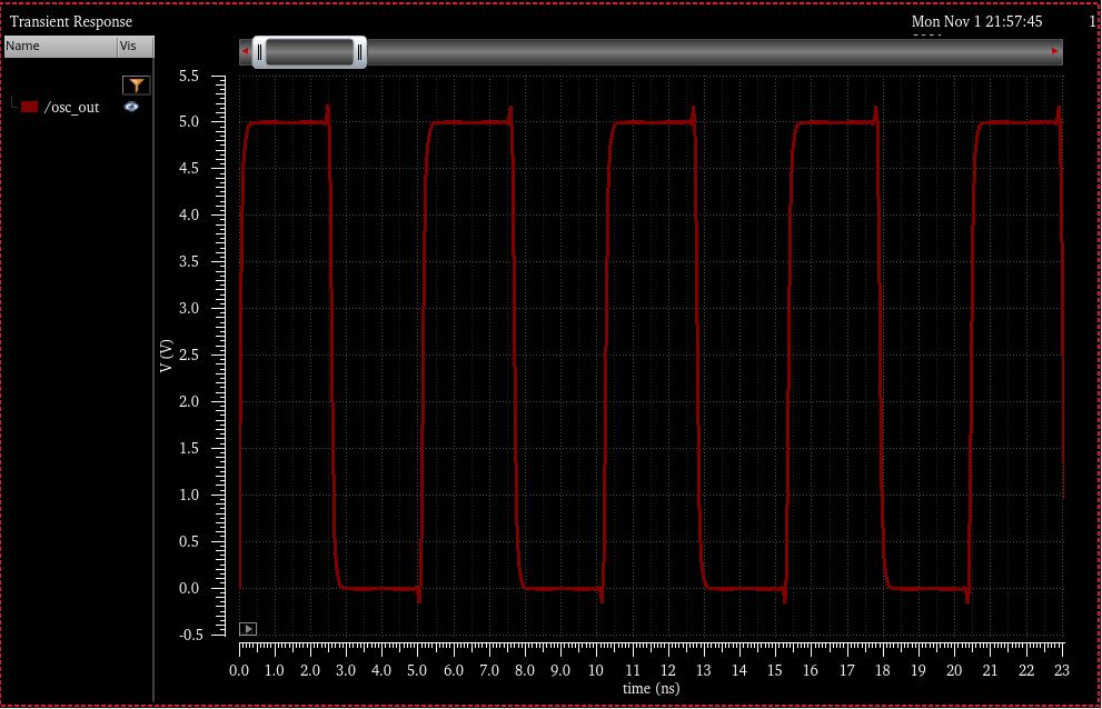
31-stage ring oscillator
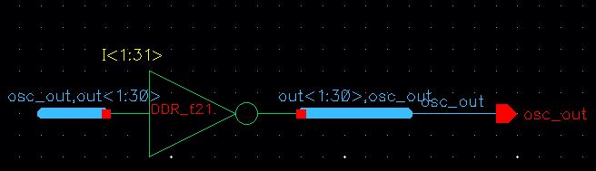
Symbol
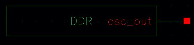
Layout
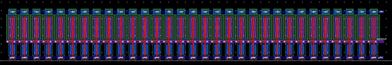
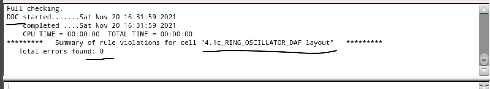
DRC
LVS
Simulation
how to test
pin 1 is the output of the ring oscillator
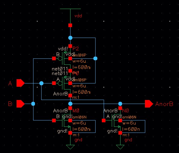
NAND and NOR gates using 6/0.6 NMOSs and PMOSs
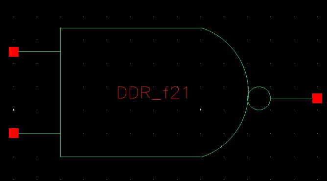
NAND GATE
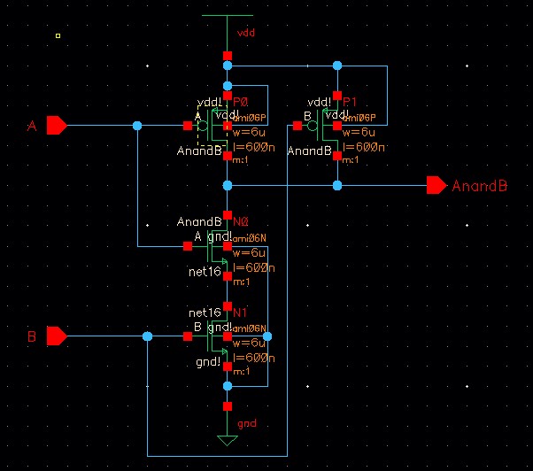
Symbol
Layout
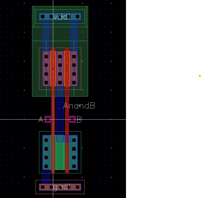
DRC
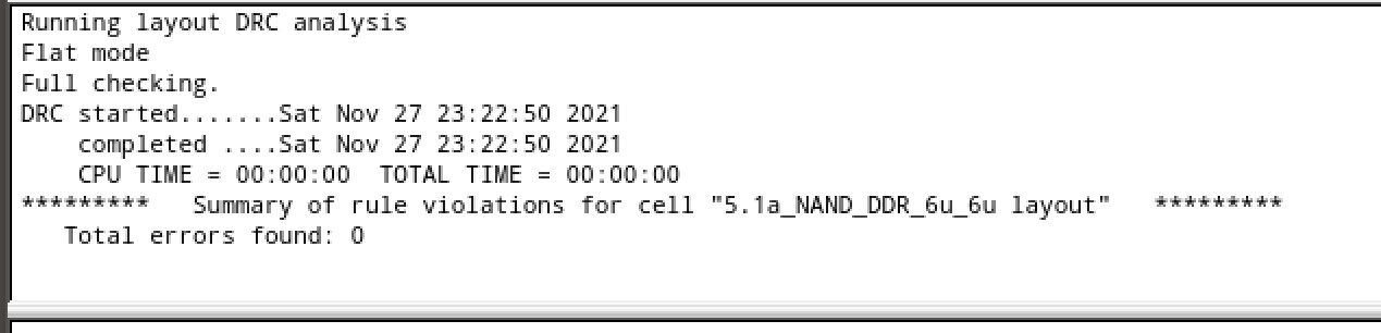
LVS
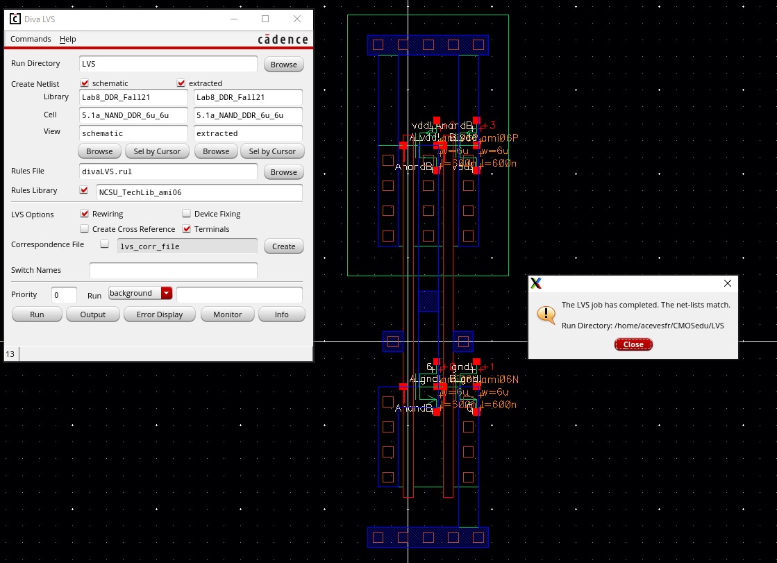
how to test
pin 22 input a and pin 21 input b, and pin 23 output of the NAND gate
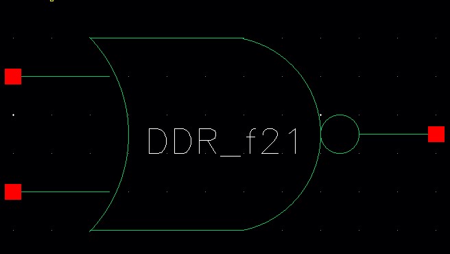
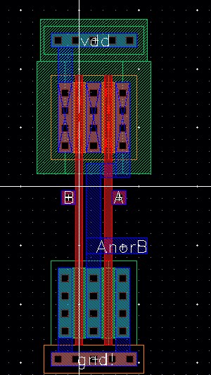
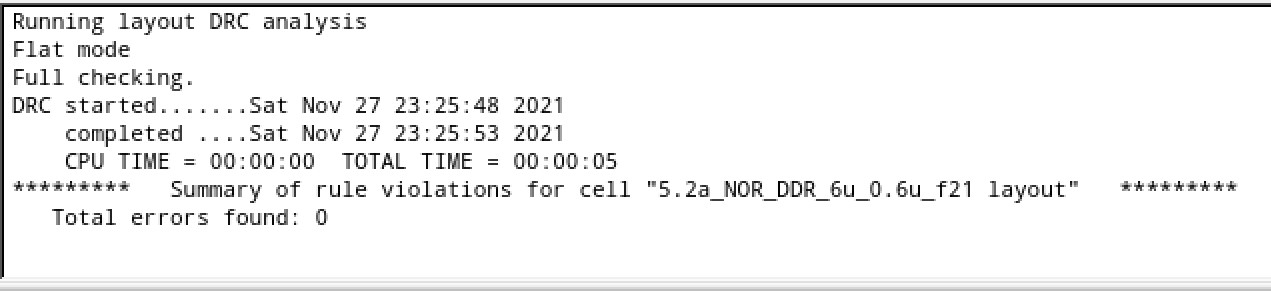
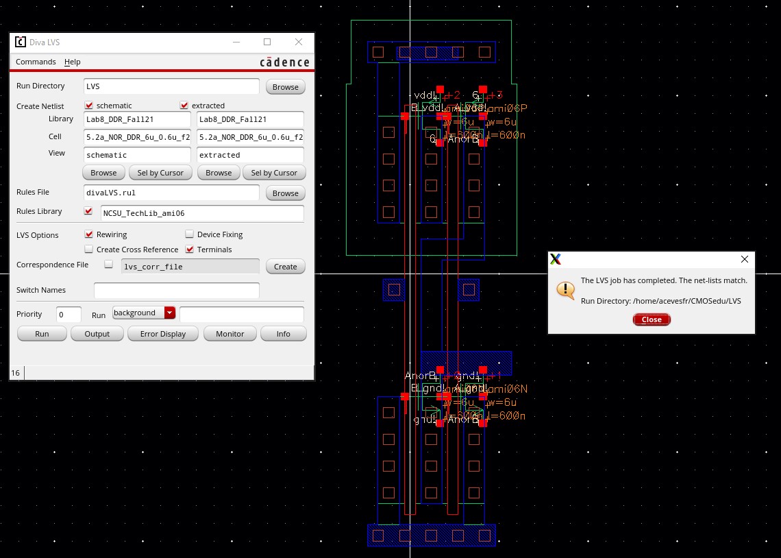
NOR GATE
Symbol
Layout
DRC
LVS
how to test
pin 24 is input a for the NOR gate, pin 25 is input b, and pin 27 is the output
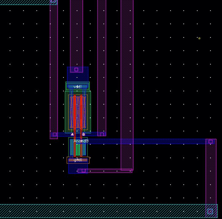
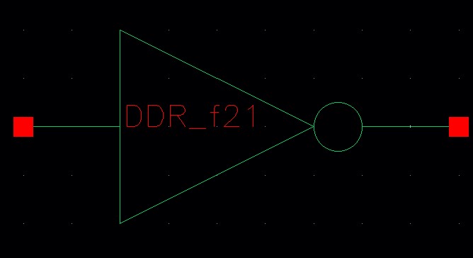
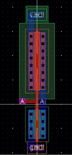
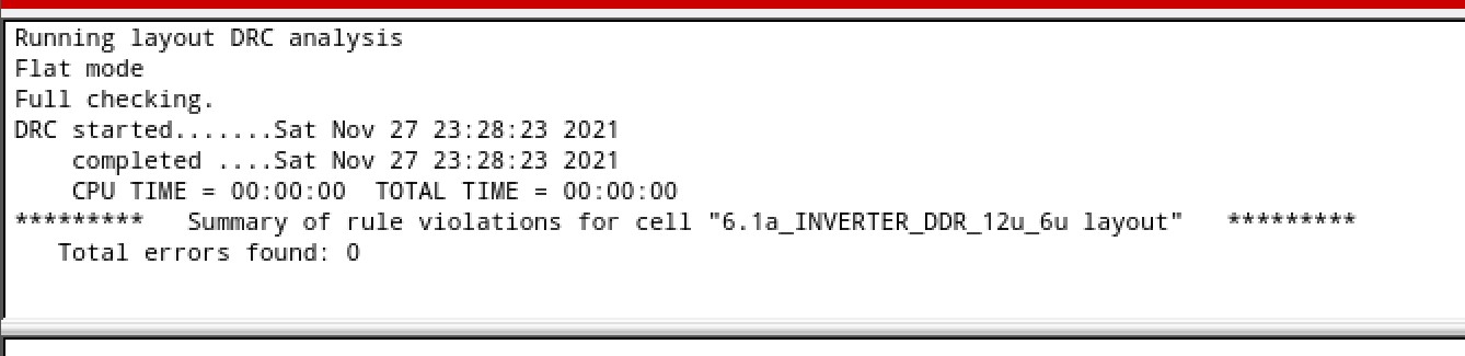
An inverter made with a 6/0.6 NMOS and a 12/0.6 PMOS
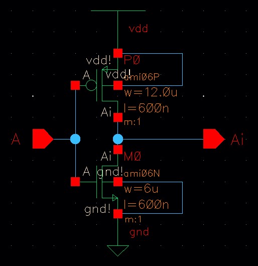
Symbol
Layout
DRC
LVS
how to test
pin 15 is the input of the inverter and pin 16 is the output of the inverter
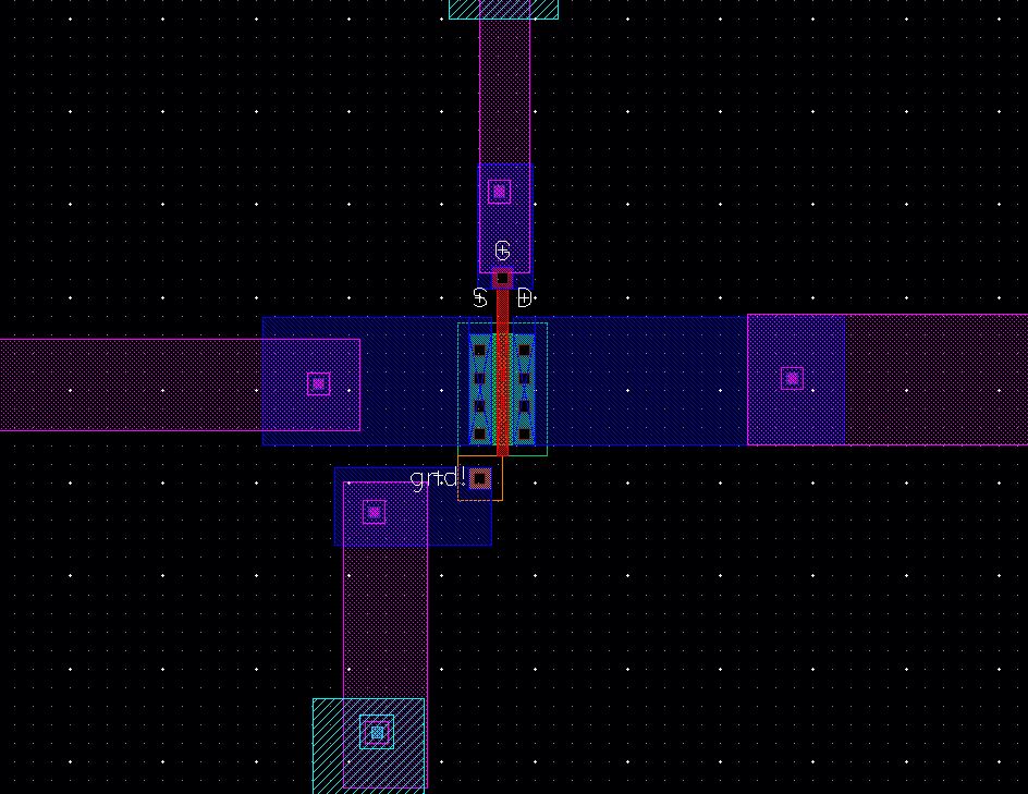
Transistors, both PMOS and NMOS, measuring 6u/0.6u where all 4 terminals of each device are connected to bond pads
NMOS
Schmatic
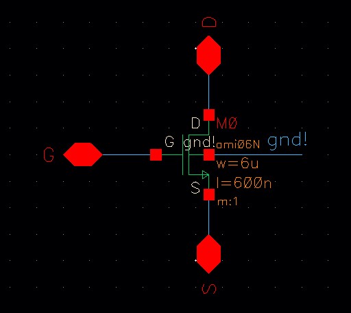
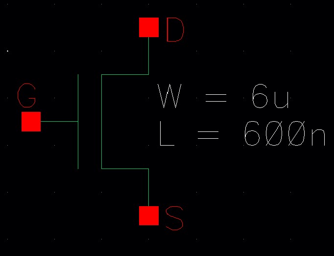
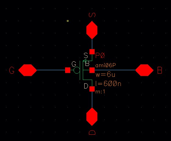
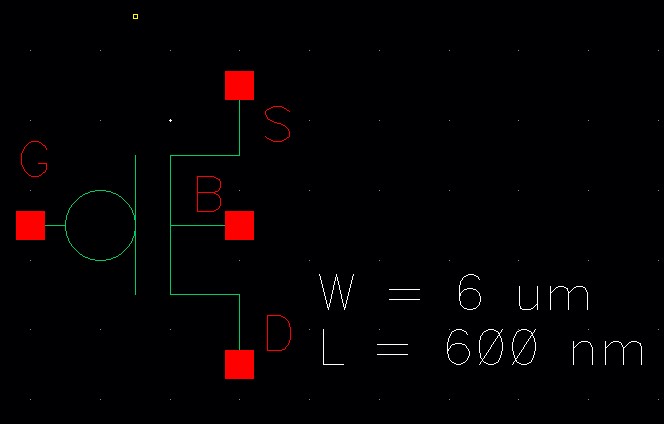
Symbol
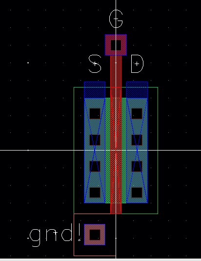
Layout
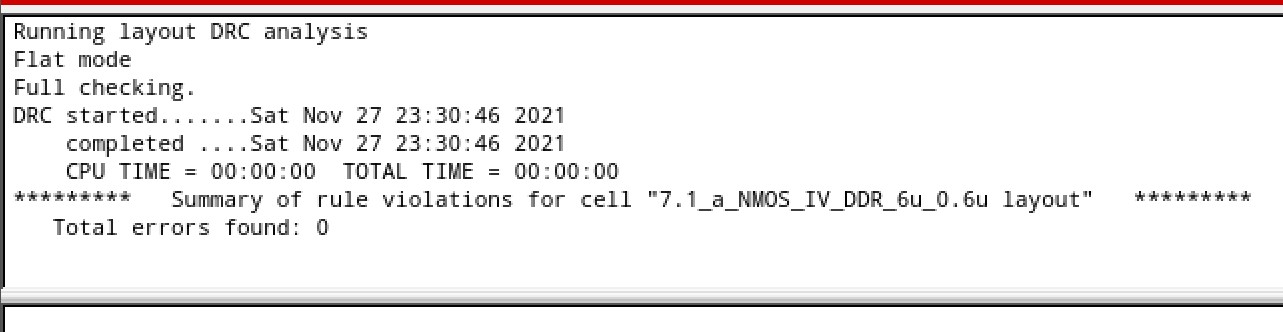
DRC
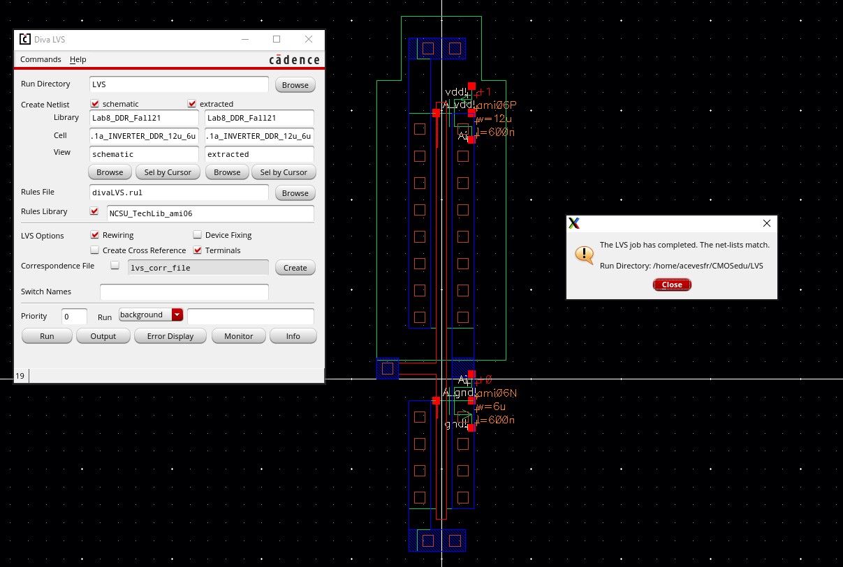
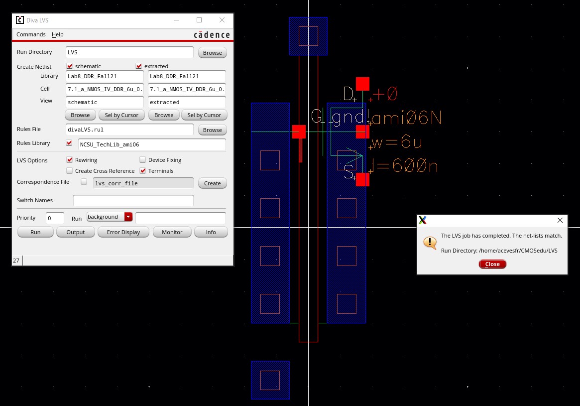
LVS
how to test
pin 7 is drain, pin 8 is the gate and pin 9 is source
PMOS
Symbol
Layout
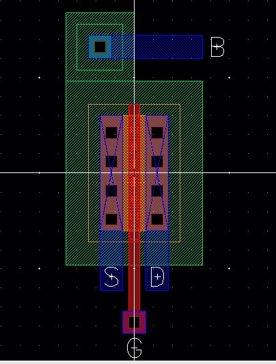
DRC
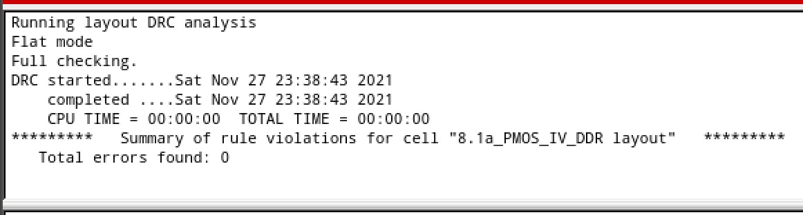
LVS
how to test.
pin 11 is source, pin 12 the gate, pin 13 drain, and pin 14 is the body of the PMOS
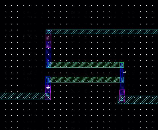
25k resistor laid out below and a 10k resistor implement a voltage divider
Symbol
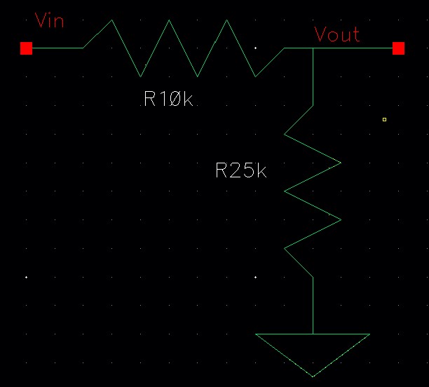
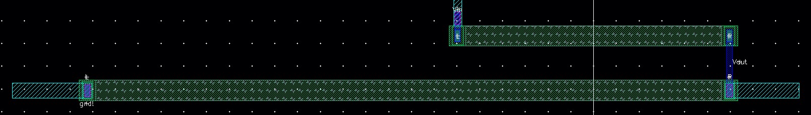
Layout
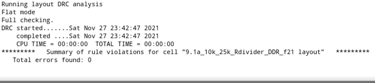
DRC
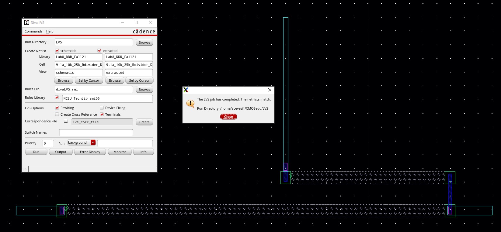
LVS
how to test.
vin is pin 5 and vout is pin 4
25k resistor implemented using the n-well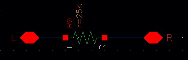
Layout

DRC
LVS
How to test.
Pin 2 and pin 3 are the resistor inputs
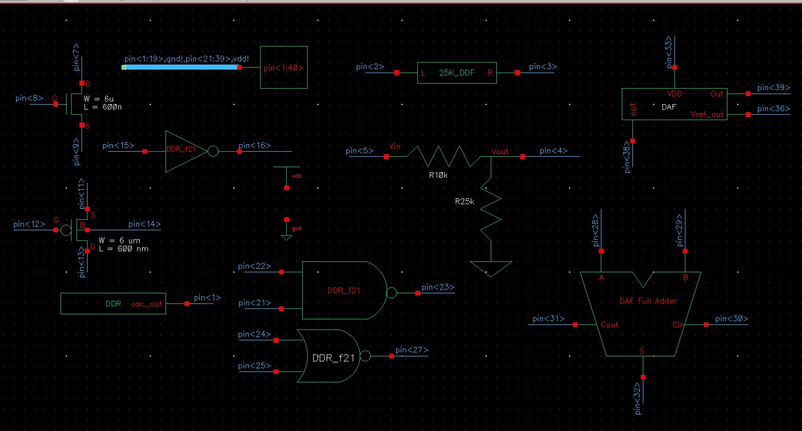
THE CHIP
Schematic
Layout
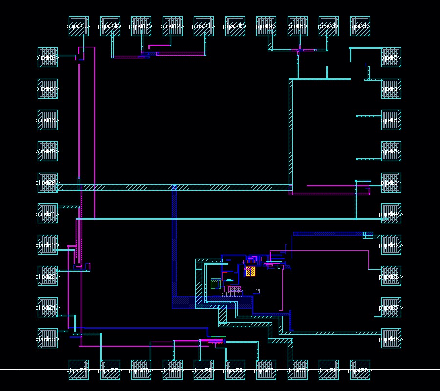
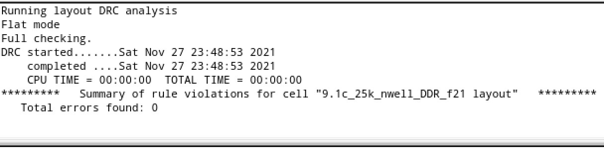
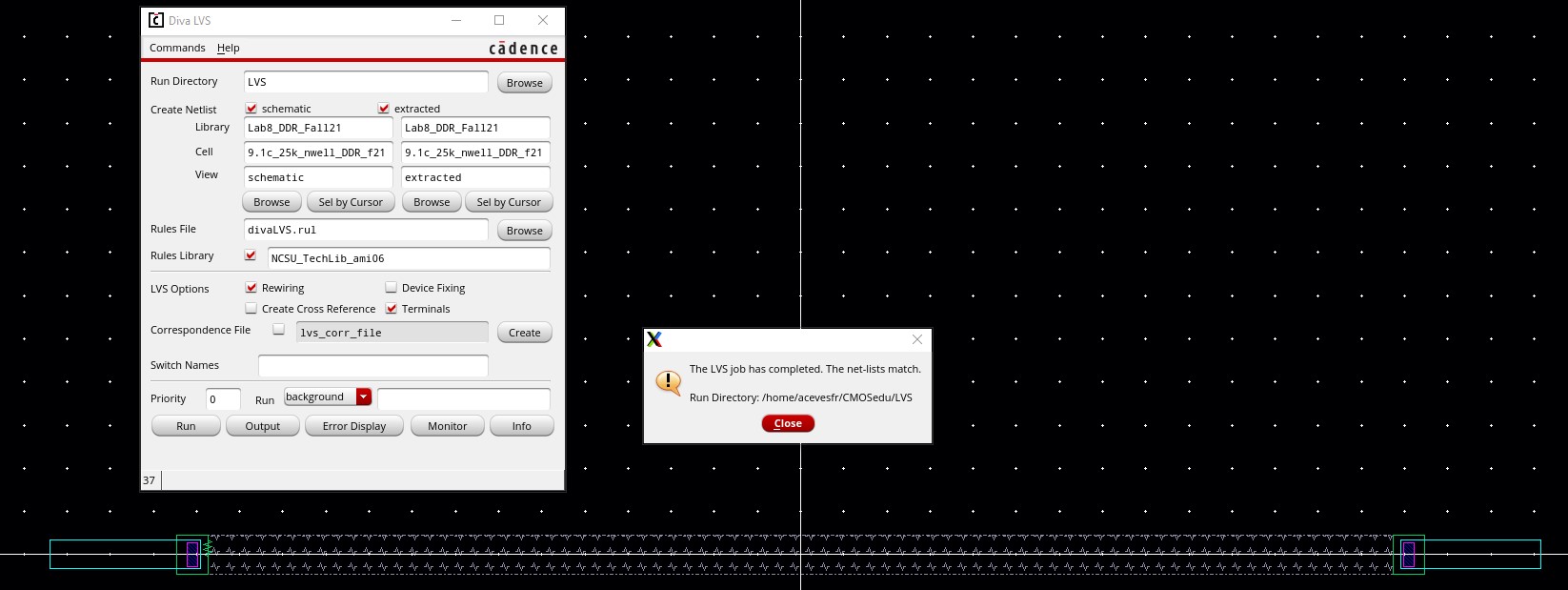
DRC
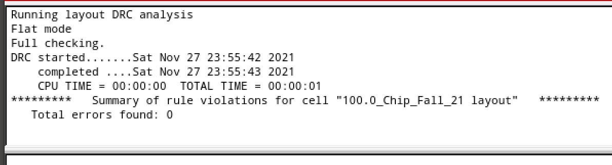
LVS
DRC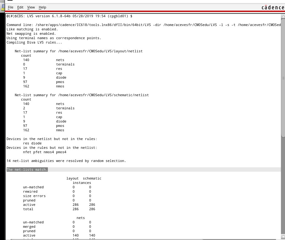
Pin 20 is ground 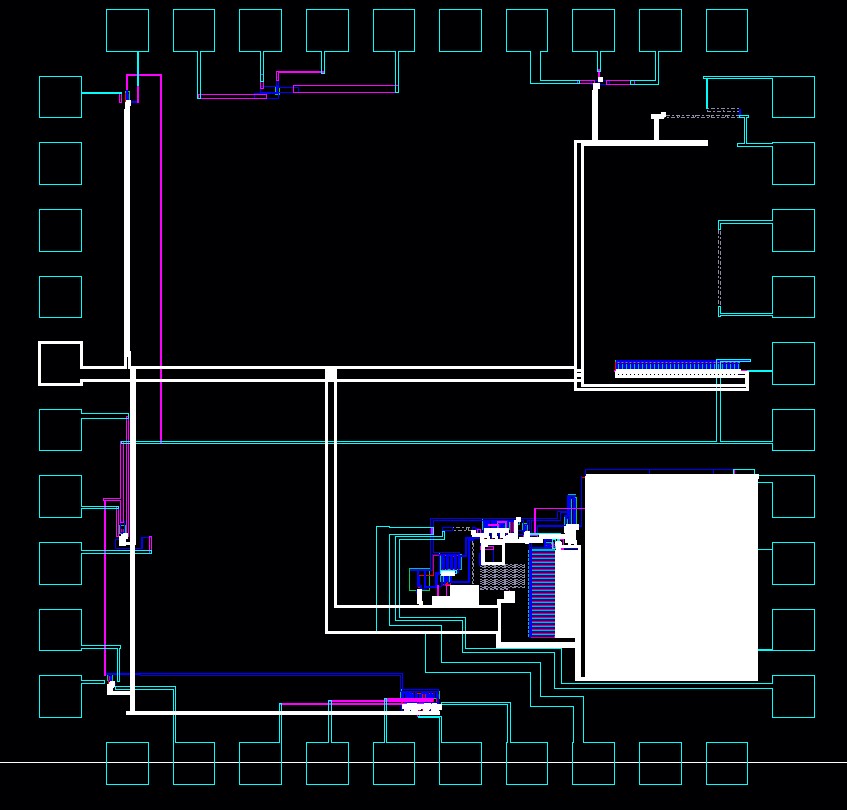
PINS
| Pin 1 | Oscillator output |
| Pin 2 | Input of 25k |
| Pin 3 | Input of 25k |
| Pin 4 | 10k||25k output |
| Pin 5 | Input of 10k |
| Pin 6 | NMOS VDD |
| Pin 7 | NMOS drain |
| Pin 8 | NMOS gate |
| Pin 9 | NMOS source |
| Pin 10 | PMOS VDD |
| Pin 11 | PMOS source |
| Pin 12 | PMOS gate |
| Pin 13 | PMOS drain |
| Pin 14 | PMOS body |
| Pin 15 | Inverter input |
| Pin 16 | Inverter output |
| Pin 17 | Inverter VDD |
| Pin 18 | NA |
| Pin 19 | NA |
| Pin 20 | Gound |
| Pin 21 | Input NAND B |
| Pin 22 | Input NAND A |
| Pin 23 | Ouput NAND |
| Pin 24 | Input NOR A |
| Pin 25 | Input NOR B |
| Pin 26 | Full Adder VDD |
| Pin 27 | Output NOR |
| Pin 28 | Input Full Adder A |
| Pin 29 | Input Full Adder B |
| Pin 30 | Cin Full Adder |
| Pin 31 | Cout Full Adder |
| Pin 32 | S Full Adder |
| Pin 33 | Set Boost Converter |
| Pin 34 | NA |
| Pin 35 | NA |
| Pin 36 | Vref Input |
| Pin 37 | NA |
| Pin 38 | VDD Boost Converter |
| Pin 39 | OUT Boost Converter |
| Pin 40 | NOR VDD and NAND VDD |
********************************************************************
Lab zip here
return to labs