Lab 7 - EE 421L
Damian Aceves Franco
acevesfr@unlv.nevada.edu
11/03/21
Using buses and arrays in the design of word inverters, muxes, and high-speed adders
Pre-lab work
- Back-up all of your work from the lab and the course.
- Go through Tutorial 5 seen here.
- Read through the entire lab before starting it.
Creating a new schematic cell, ring_osc, with one inverter
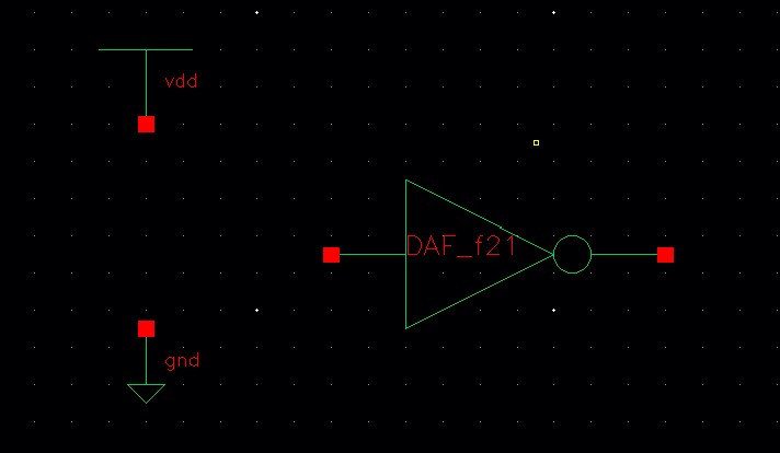
Pressing bindkey c and clicking on the Inverter
Repositioning the first inverter to get the following

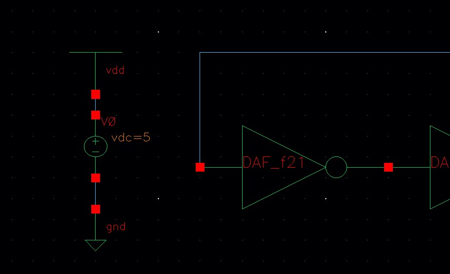
Placing labels and the DC Voltage supply
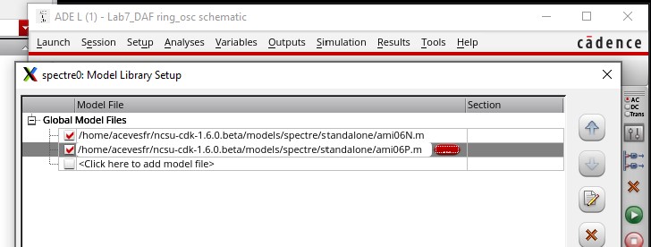
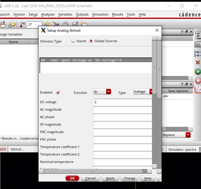
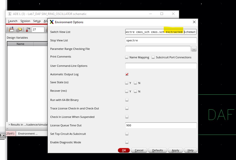
Now, setting up the ADE, libraries
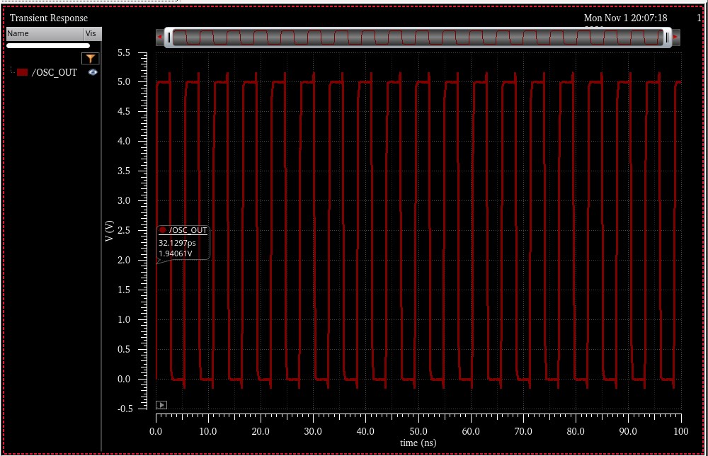
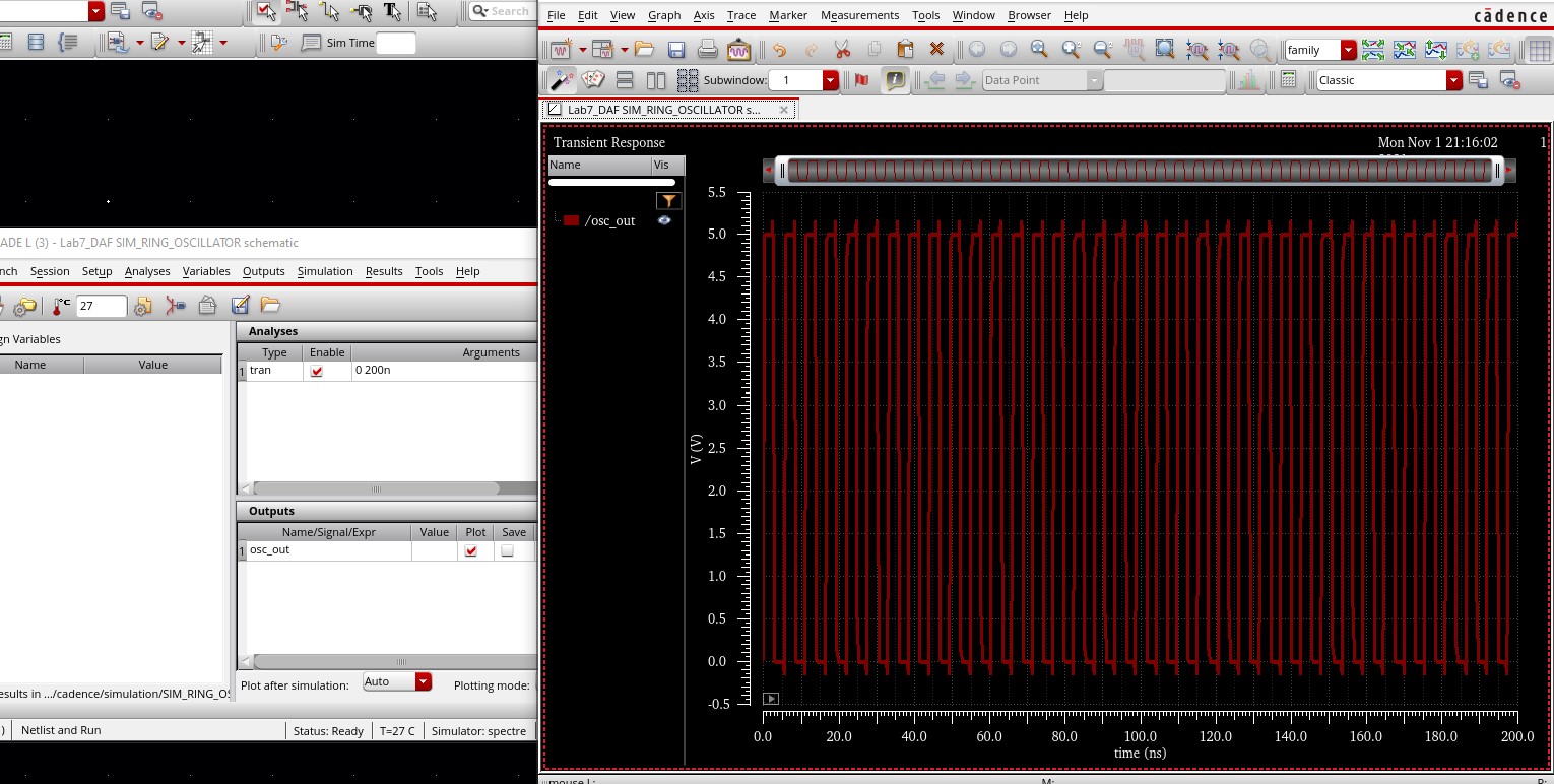
Transient
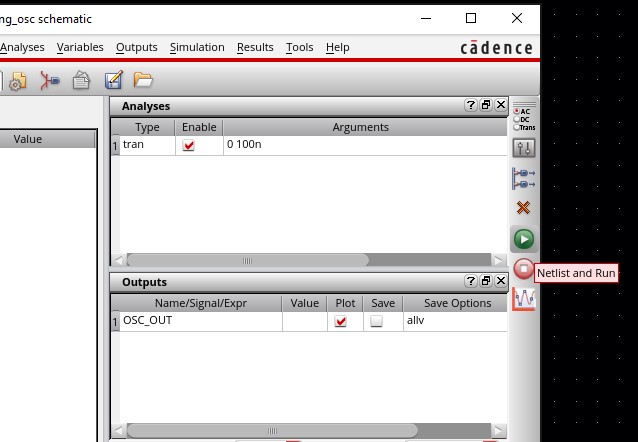
Inital results
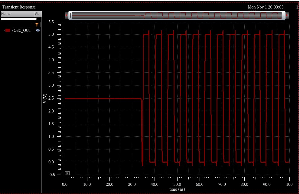
Noise will kick start this
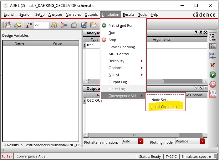
We have to set the initial condition at the input of the first inverter to 0
In the ADE, Simulation -> Convergence Aids -> Initial Condition
Set the Node Voltage to 0
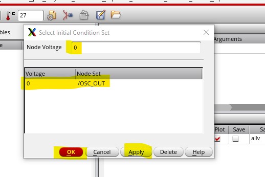
Check and save, and rerun the simulation
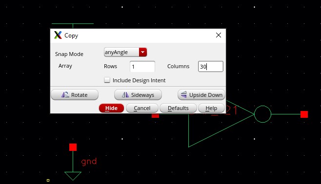
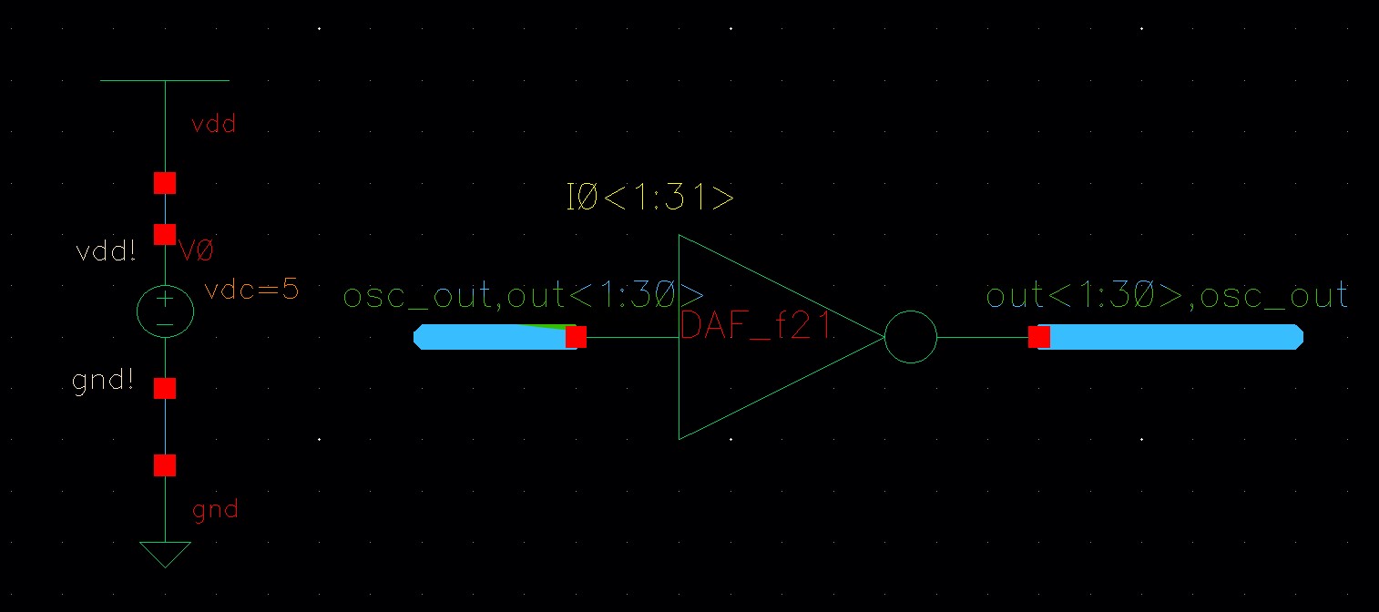
With the same schematic, we can make this ring oscillator look neater by
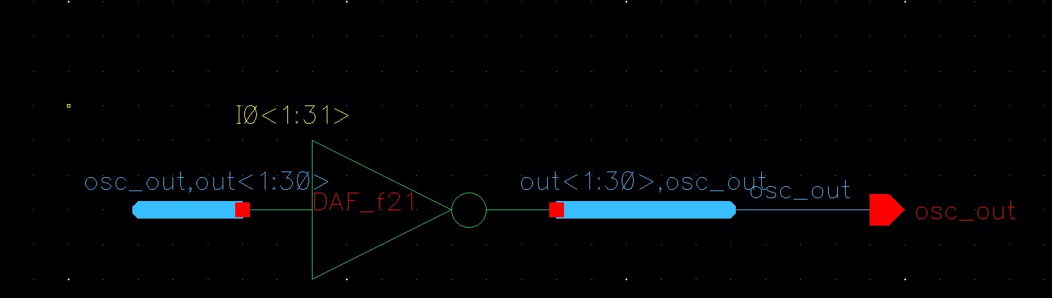
Deleting all of the inverters except the first inverter and changing the name of the inverter to I0<0:30> or I0<1:31>
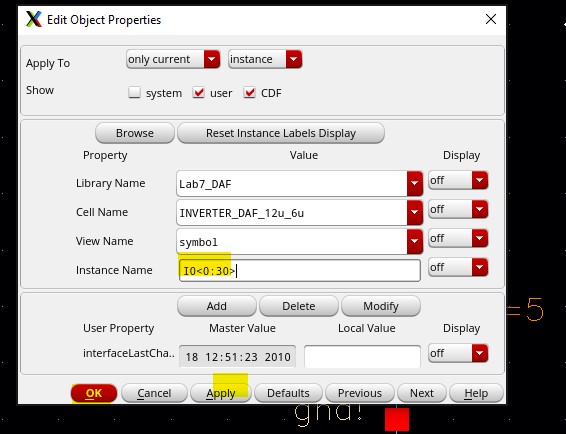
Using bindkey Shift+W to create a wide wire bus wire on the input and output of the inverter
Close all cell views
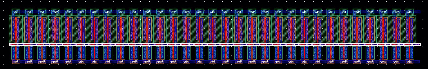
Now, creating a layout for our ring oscillator
Instantiating our inverter layout
Copying and pasting the 2nd inverter
F3 and paste
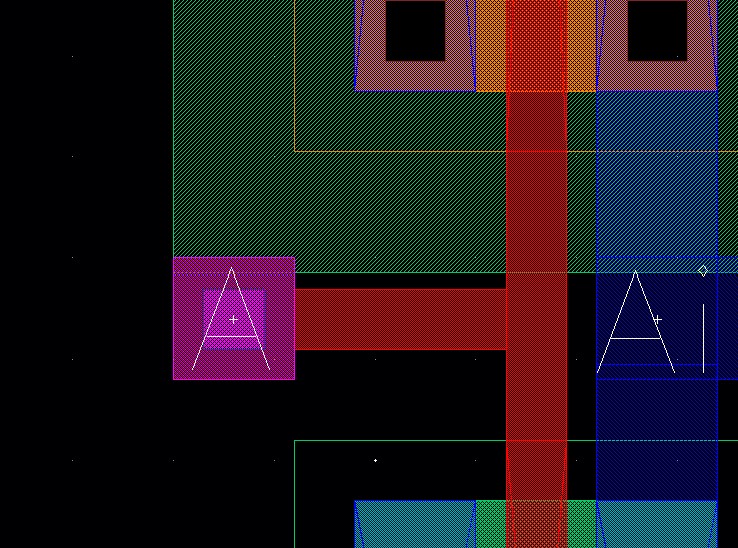
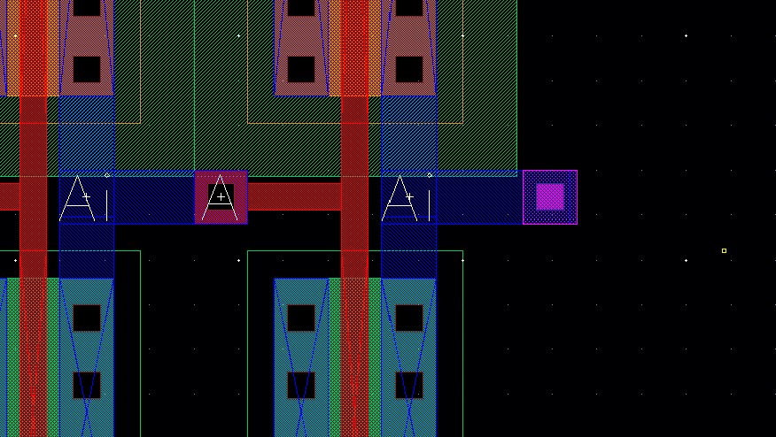
Make connection as below
Copy out
Place via on the 1st one
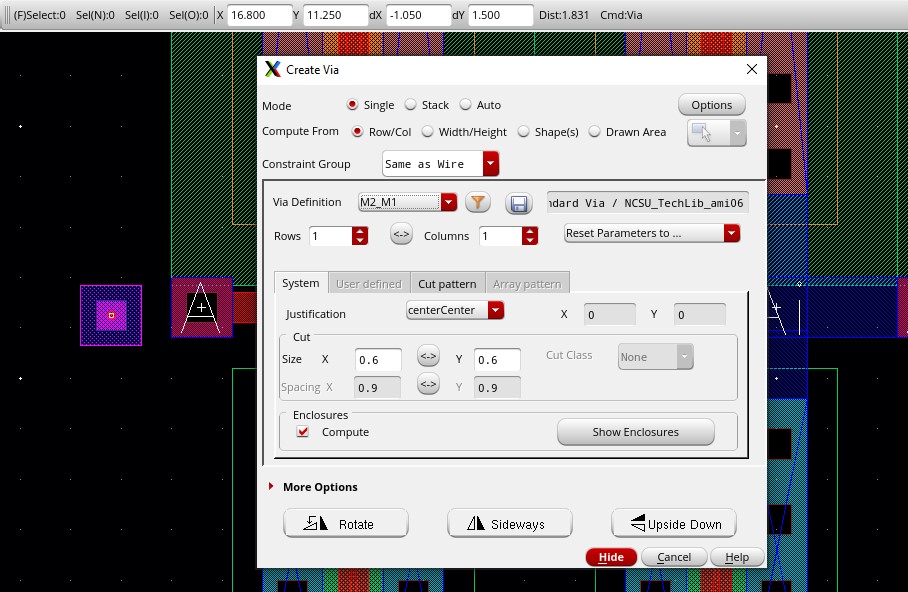
And via at the last one
Using metal 2 to connect the 1st to the last as the schematic
DRC
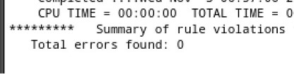
Extract
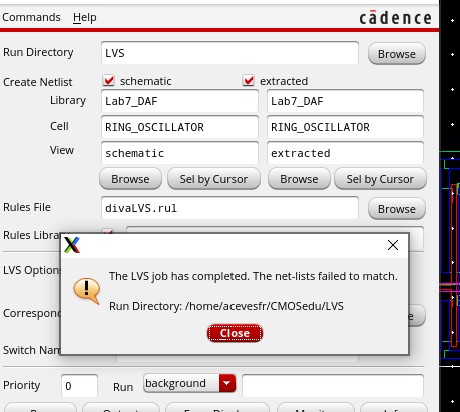
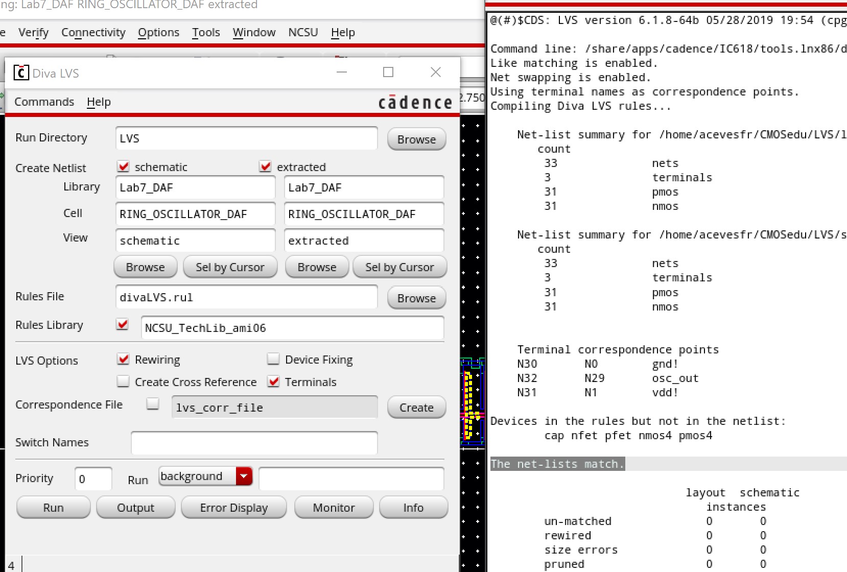
LVS
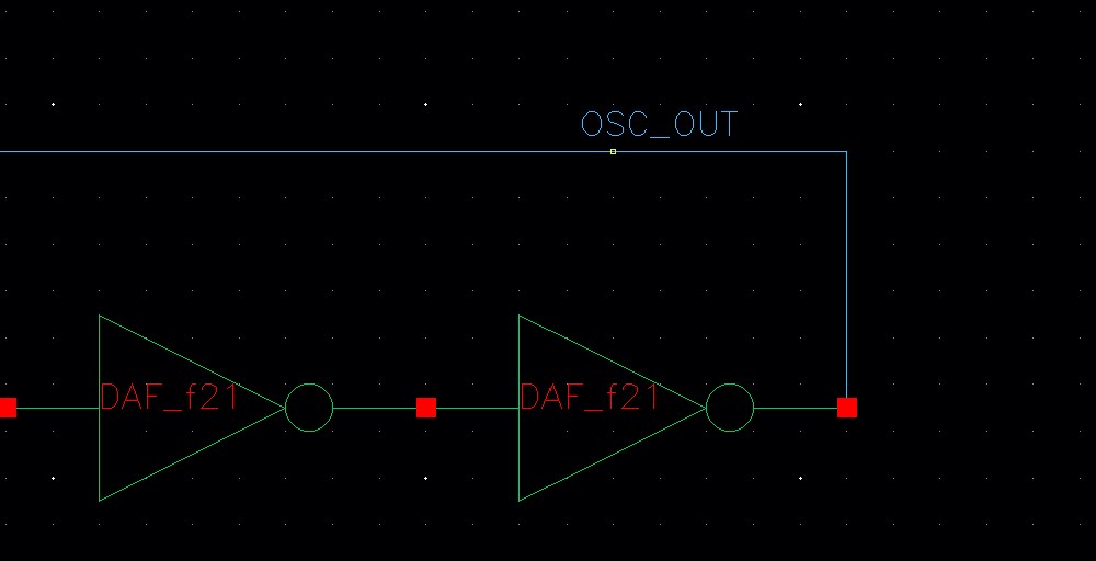
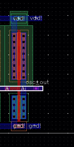
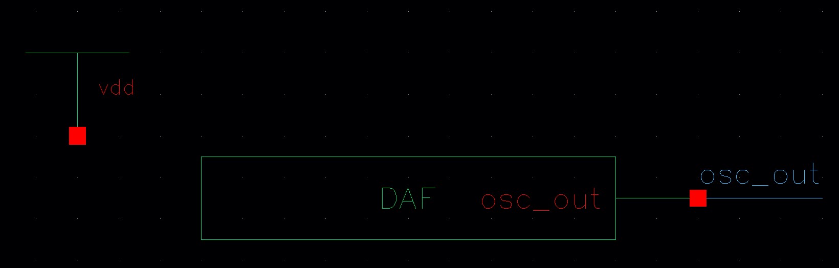
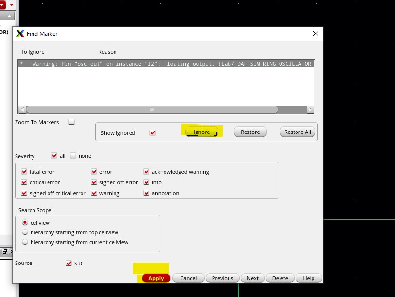
Recalling that we need to have a pin, osc_out in our schematic
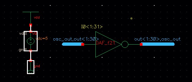
and remove the DC power too
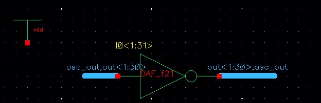
Leaving it as follows
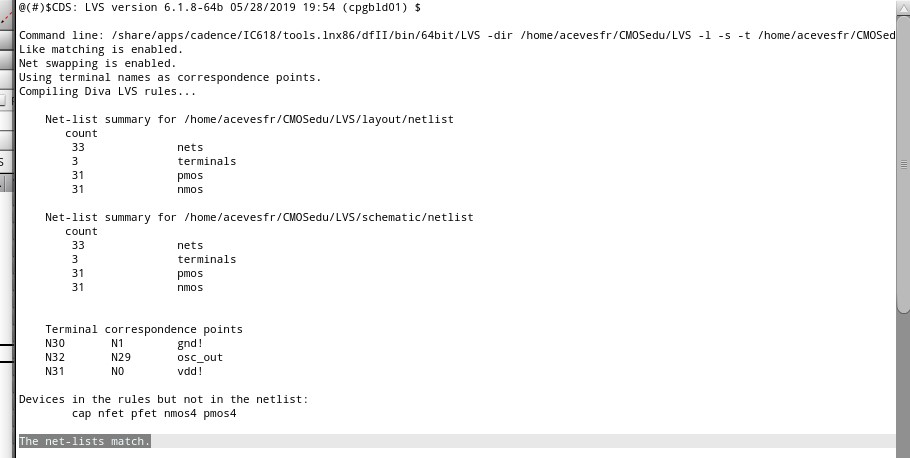
Rerun LVS
Creating a symbol and Creating a schematic
We will resimulate the ring oscillator
Now,
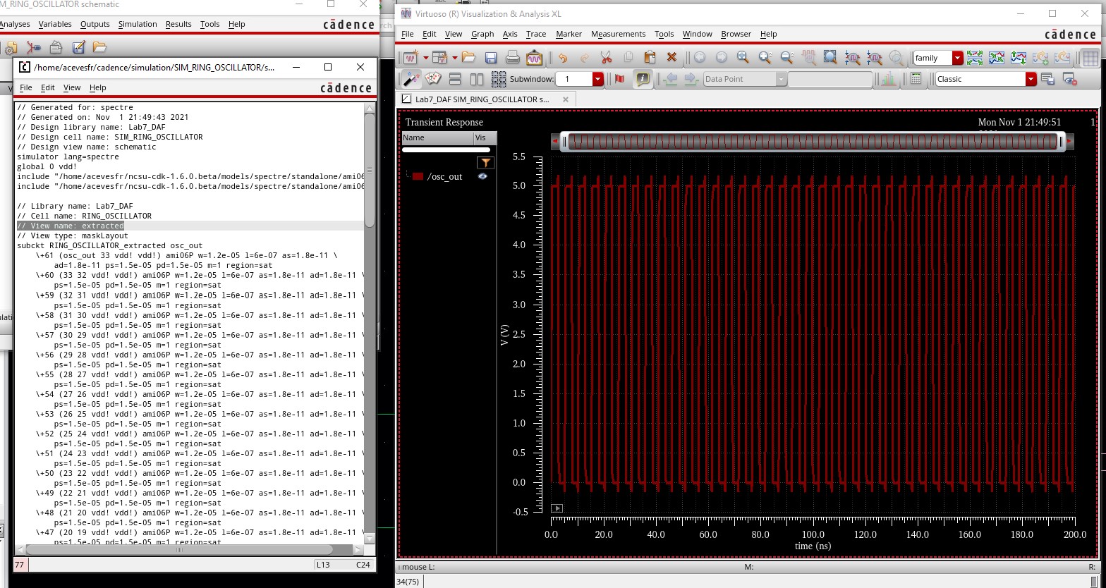
lets simulate the layout. Since the LVS passed (the extracted view’s
nodes match the schematic view’s nodes), we should get the same output
Checking that it ran the extracted view (Simulation -> Netlist -> Display)
End of Prelab
******************************************************************************************************************
Experiment 1: Creating a 4-bit word inverter, with simulation
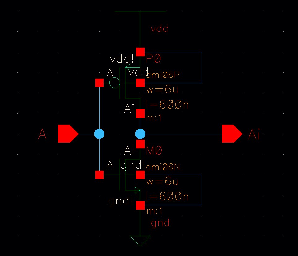
For this lab, we will need 6u/600n PMOS/NMOS inverters
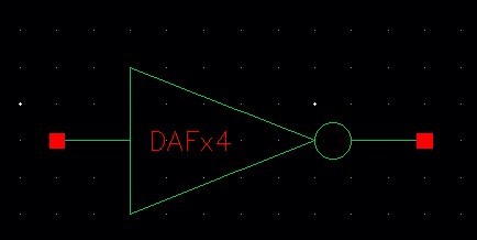
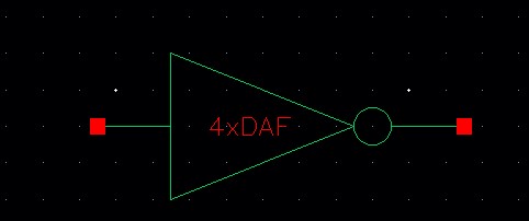
Symbol
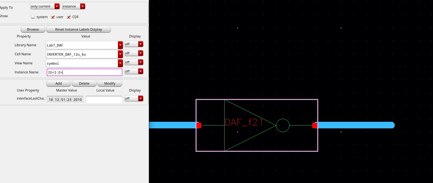
Creating a cell, inverter_4_bit
symbol
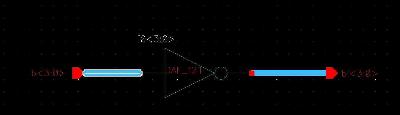
Creating a schematic
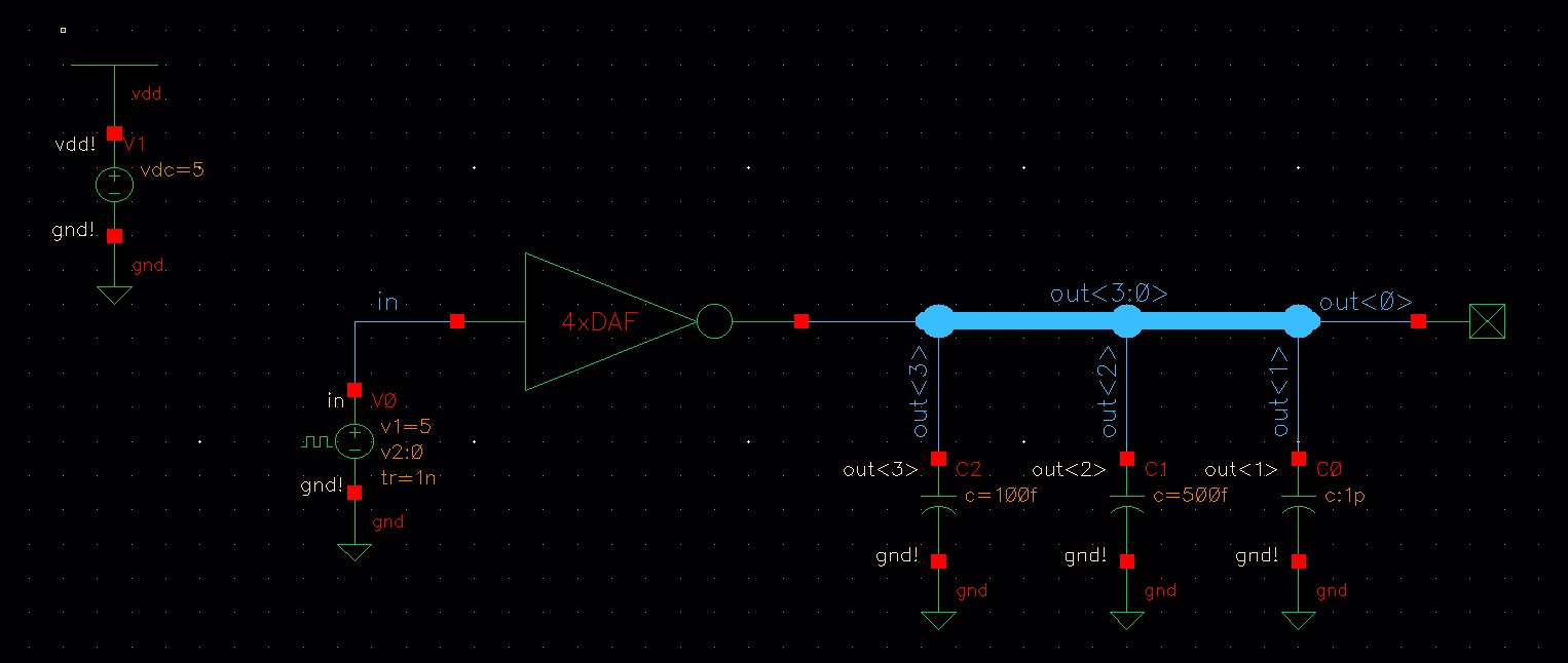
ADE setup
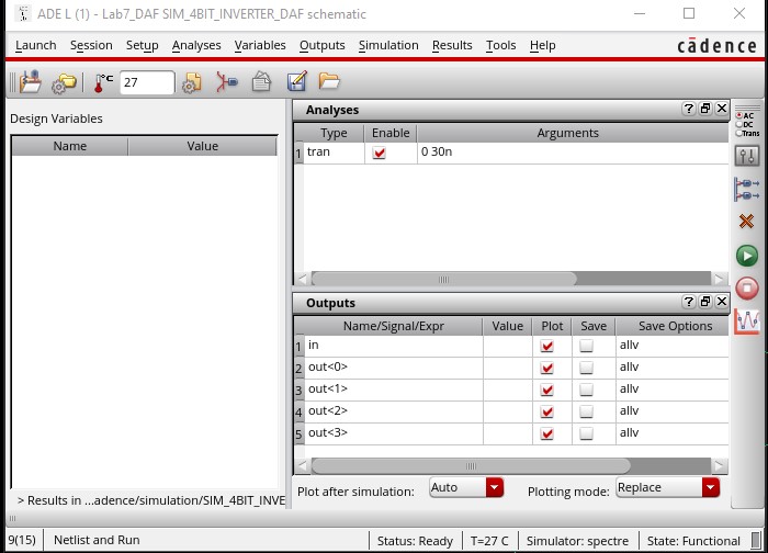
Simulation
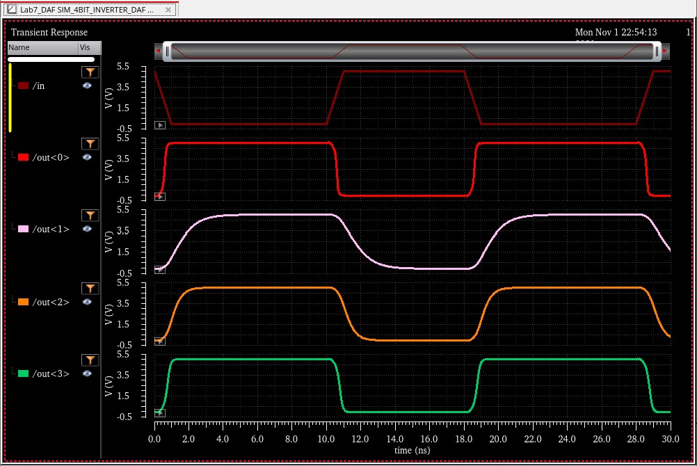
Out<0> has no load, therefore, the rise and fall time are fast. Out<1> has the heaviest load (big capacitor relative to others),
giving it a higher RC time delay. Note that the tPLH is greater since when the input is LOW, the PMOS is turned ON and has a
higher effective resistance than the NMOS, therefore, we have a larger Time Constant.
Experiment 2: Schematics and Symbols of: 8-Bit Input/Output array of NAND, NOR, AND, Inverter, and OR gates
NAND Gate
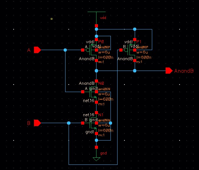
First, creating a schematic cell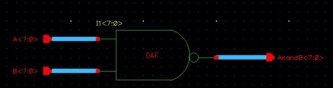
8-bit word symbol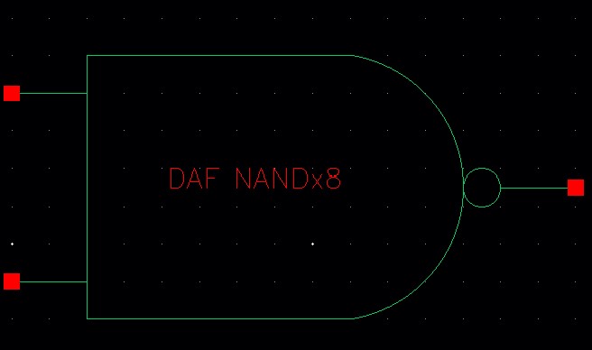
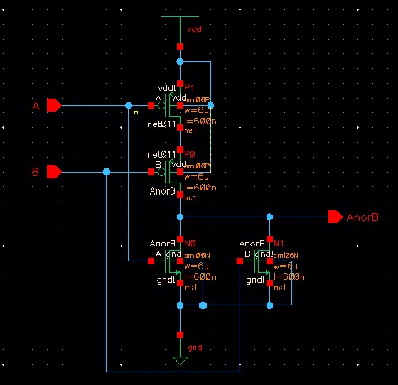
NOR Gate
Schematic of NOR gate
symbol and 8-bit word schematic
8-bit word symbol
AND Gate
We will just take the NAND gate and throw it through an inverter to make it an AND gate and 8-bit word schematic 
8-bit word symbol
Inverter
Just as similar to the first part of this lab
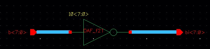
8-bit word symbol

OR
We will just take the NOR gate and throw it through an inverter to make it an OR gate and 8-bit word schematic
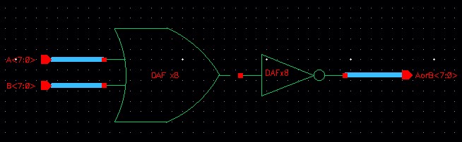
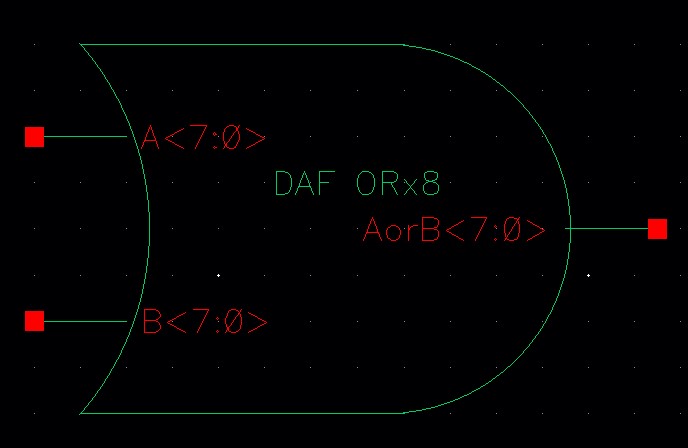
8-bit word symbol
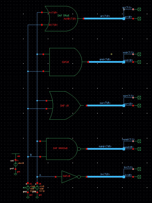
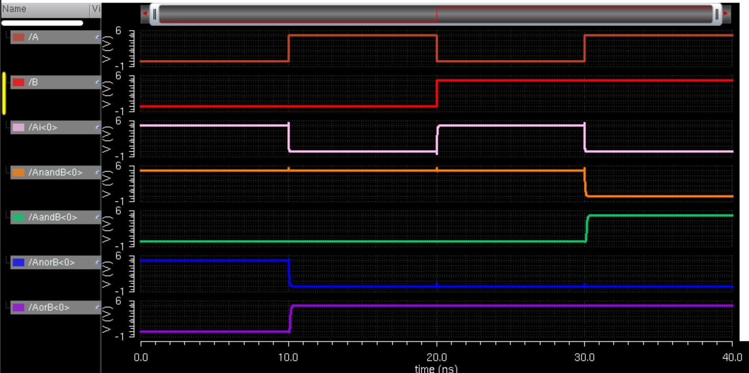
Simulaton of all gates
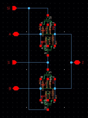
Experiment 3: 2-to-1 DEMUX/MUX
First, lets do the 2:1 MUX
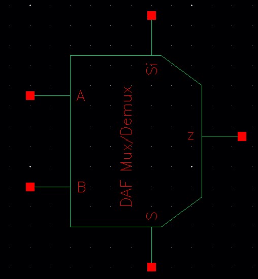
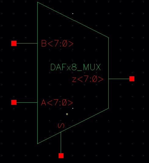
Symbol
schematic cell
8-Bit Word Schematic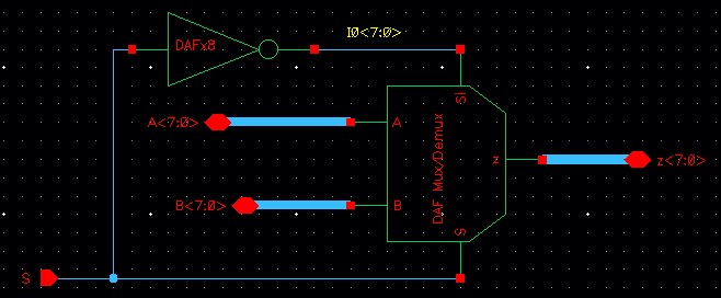
8-Bit Word Symbol
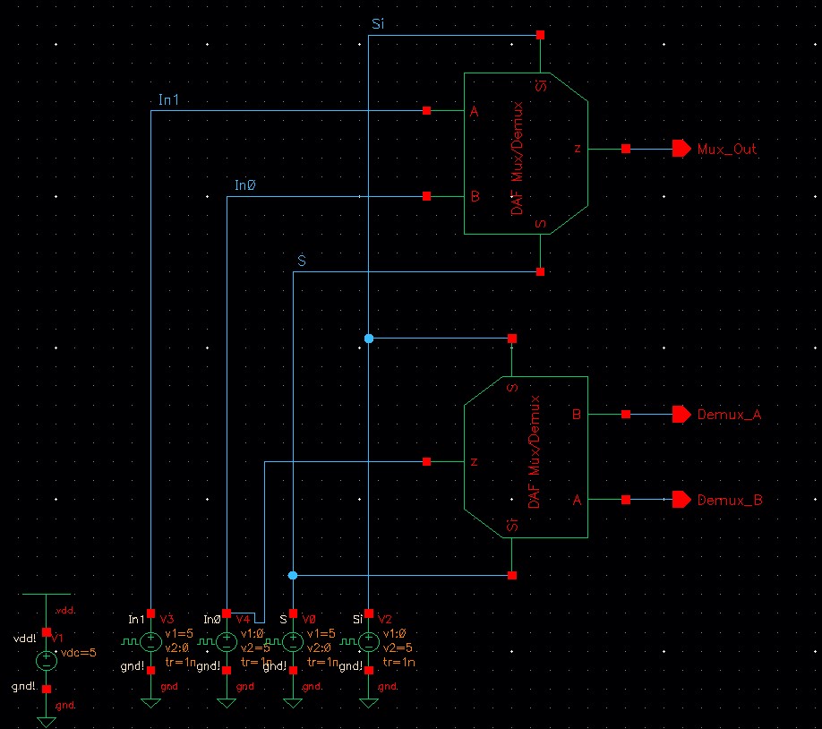
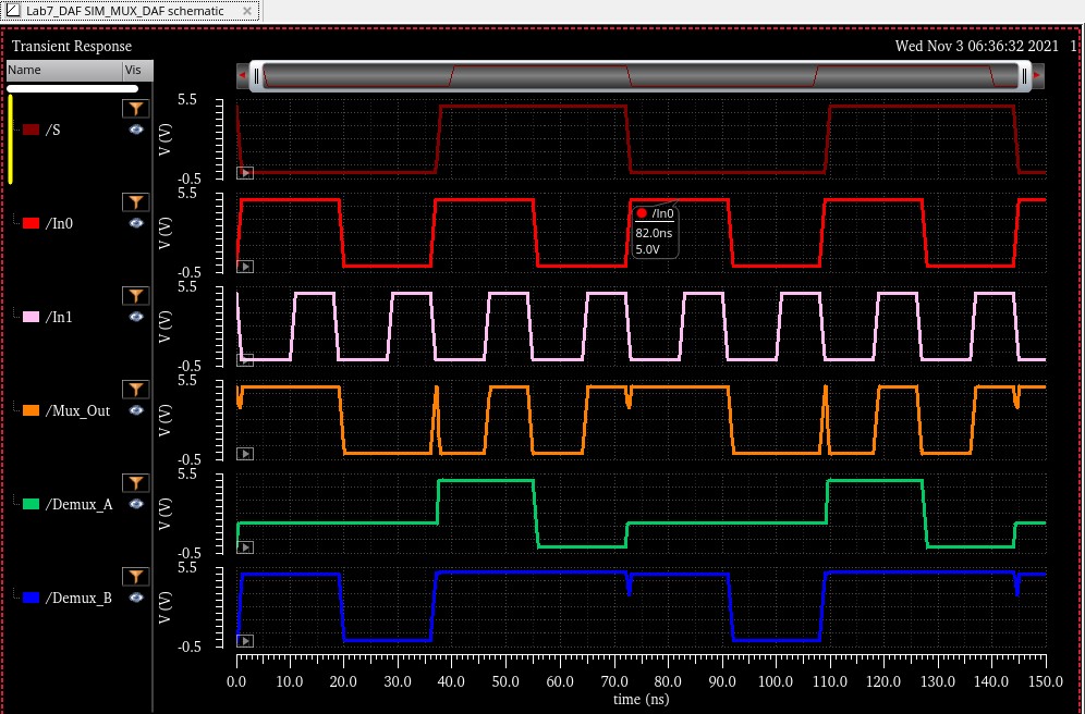
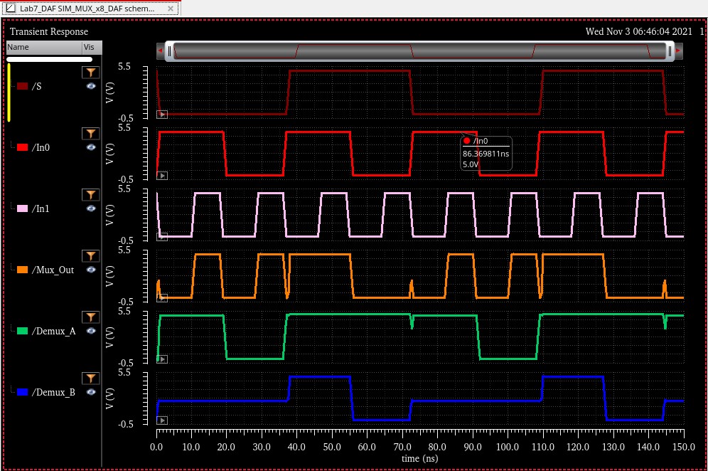
Simulation of Just the Mux
schematic cell
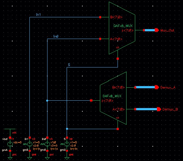
Simulation of 8 work Mux
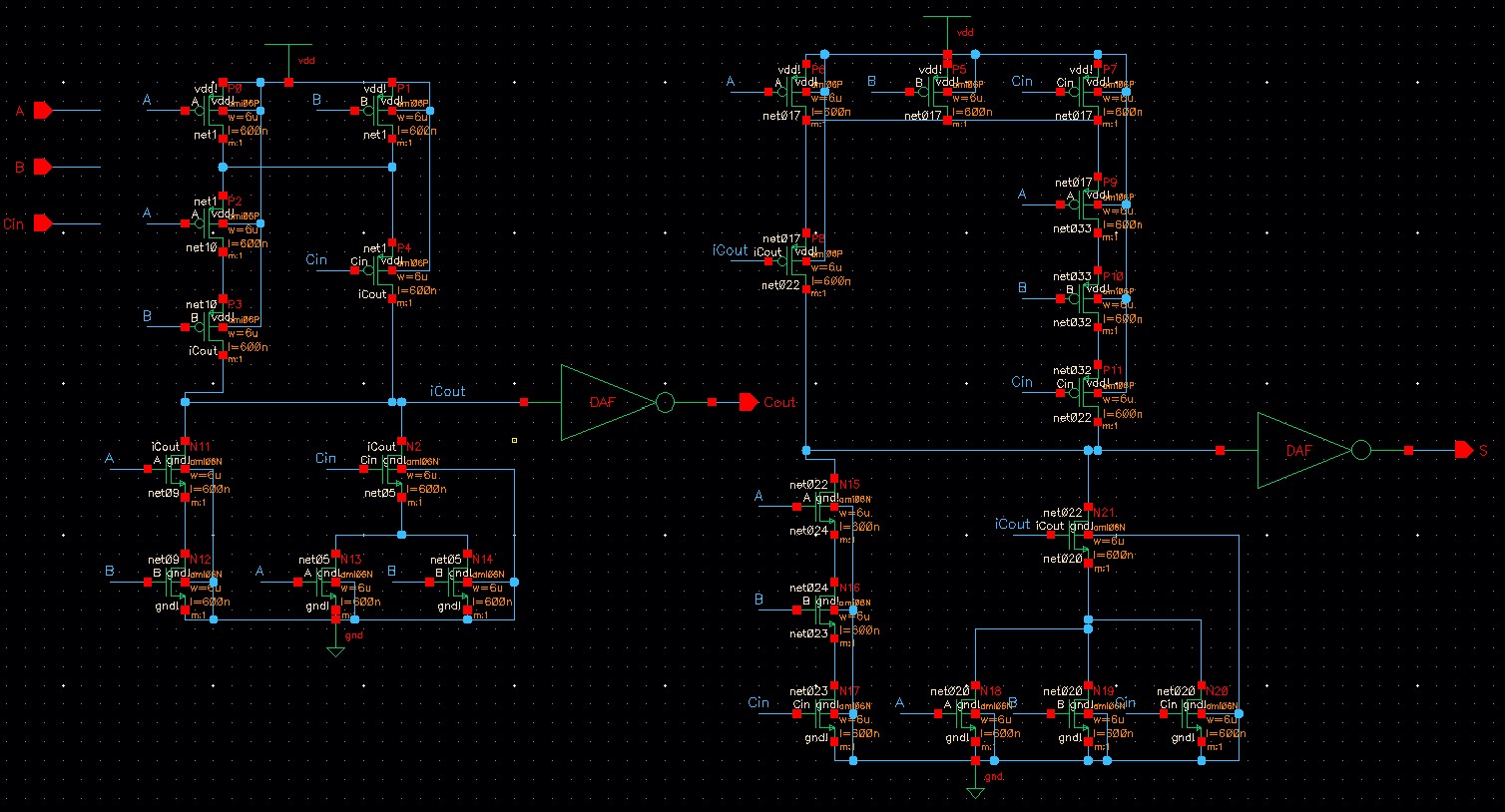
Experiment 4: The Full-Adder
schematic
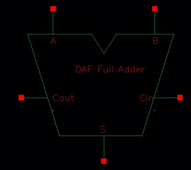
Symbol
8-Bit Word Adder Schematic
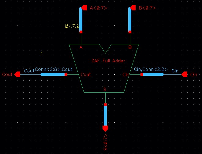
8-Bit Word Symbol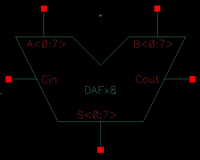
schematic for sim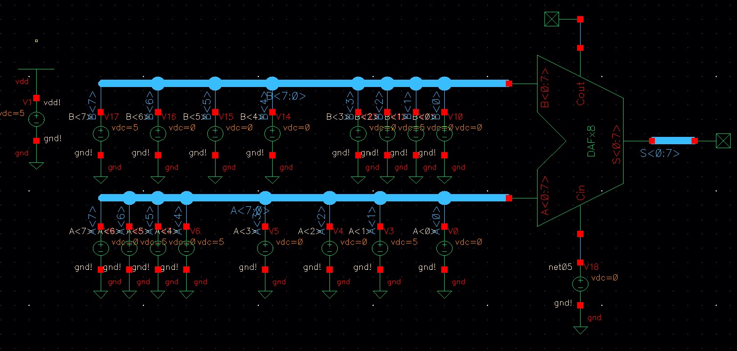
Results
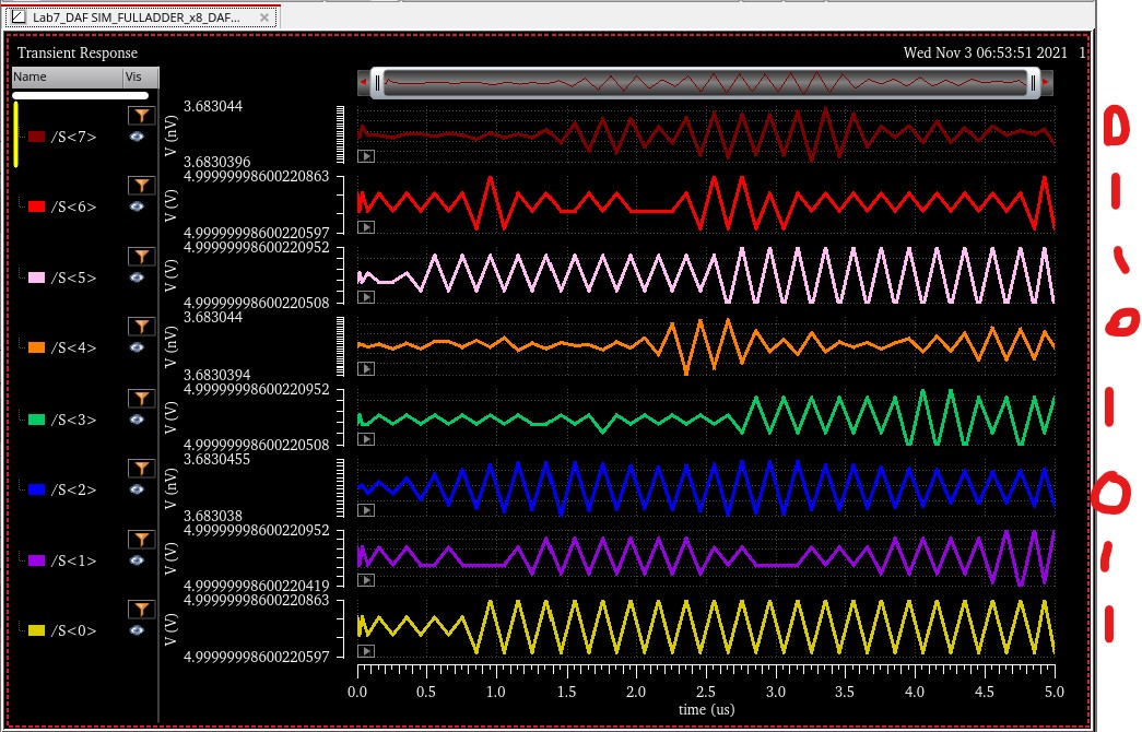
A<01001010> +B< 00100001>
A + B = 01101011
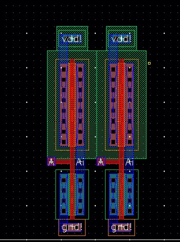
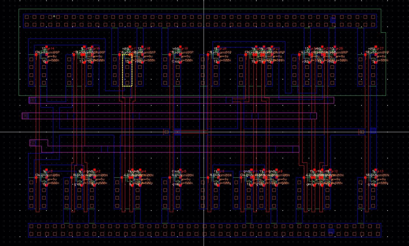
Layout of the Full Adder
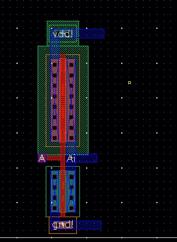
1-bit Full Adder
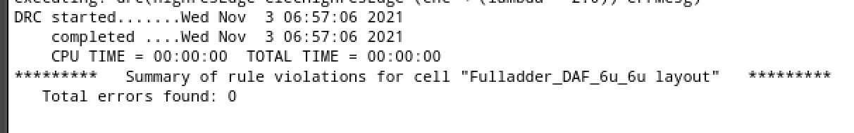
DRC
Ectraction
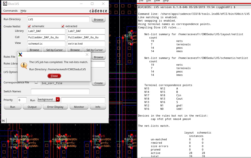
LVS
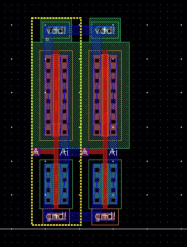
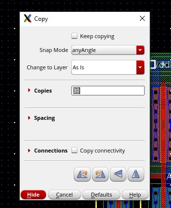
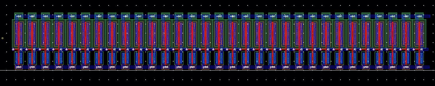
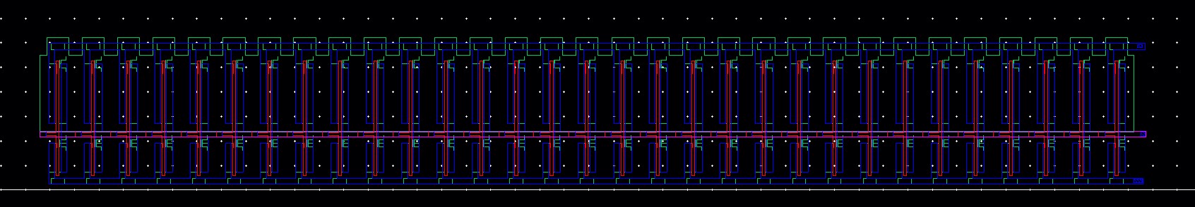
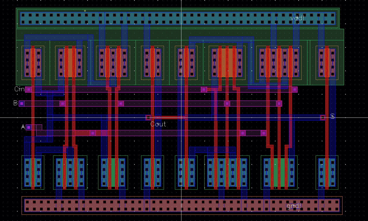
Laying out the 8-Bit Full Adder

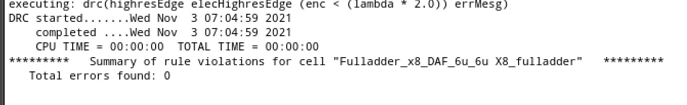
DRC
Ectracted layout
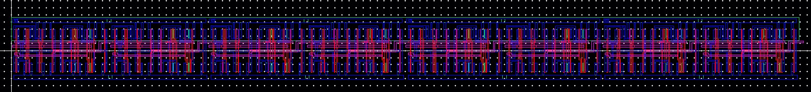
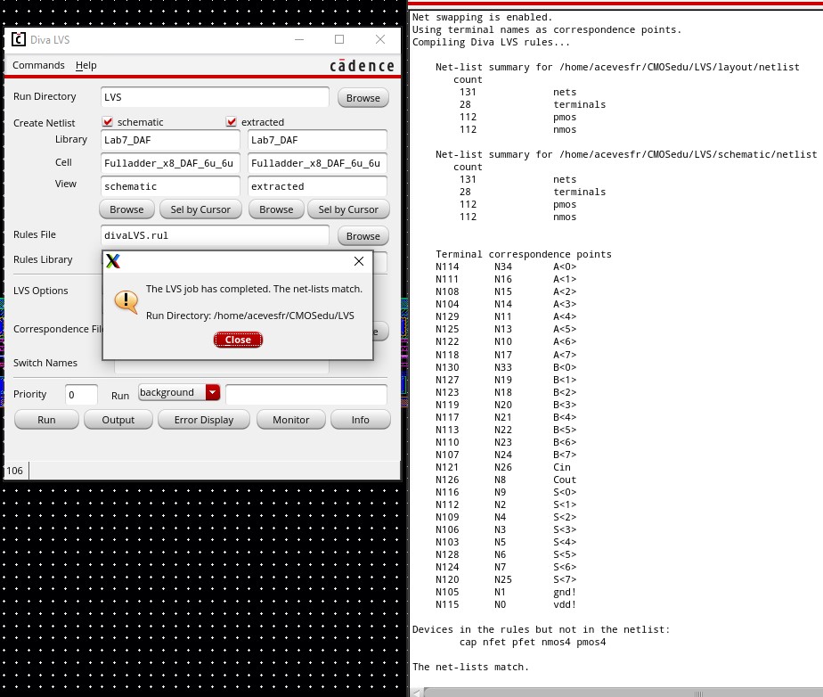
LVS
End of lab
backup
Return to Labs