Lab 6 - EE 421L
Damian Aceves-Franco
acevesfr@unlv.nevada.edu
10/05/2021
October 6 – Lab6 – Design, layout, and simulation of a CMOS NAND gate, XOR gate, and Full–Adder, due October 20
************************************************************************************************
Pre-Lab Work
- Back-up all of your work from the lab and the course.
- Go through Cadence Tutorial 4 seen here.
- Read through the lab in its entirety before starting to work on it
Creating a cell with scemaitc
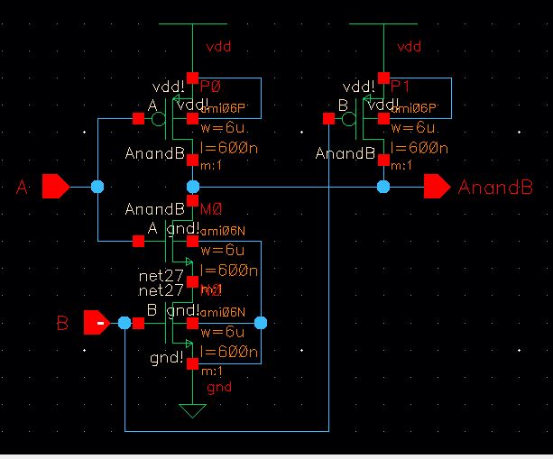
2-Input NAND Gate Schematic
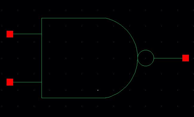
Symbol

Create a new schematic, sim_nand2_tran, and do the following
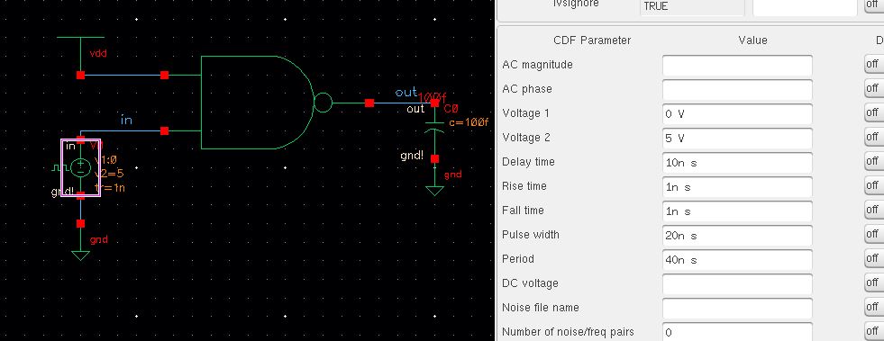
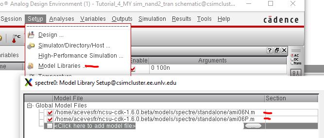
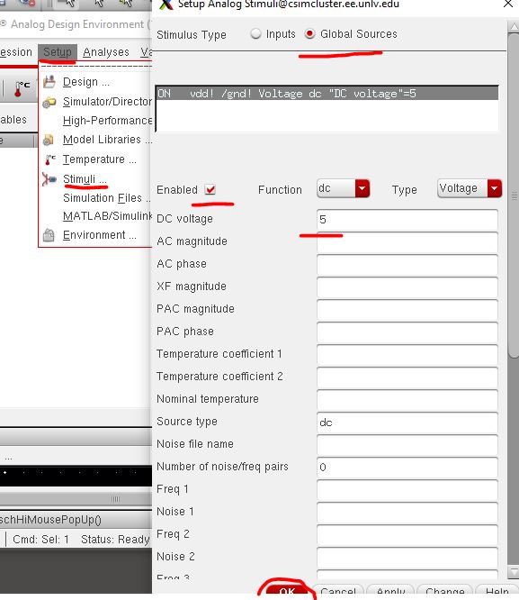
Launching the ADE, and setting up the simulator
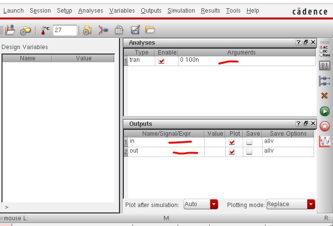
Output
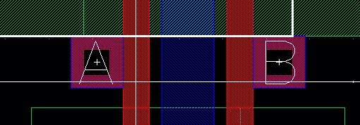
Layout
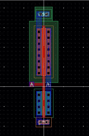
Copy/Paste and move the block closer to each other Combine them
Final result
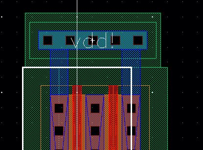
Create Pins
Vdd
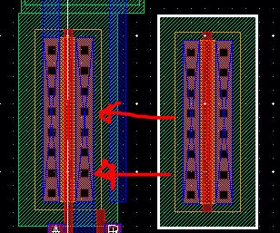
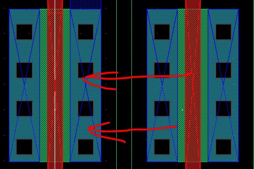
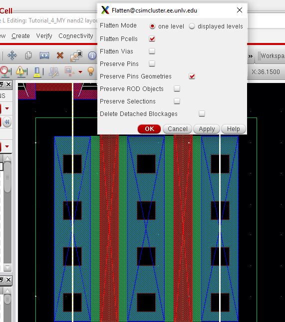
Looking at the NMOS portion we must use Flattening out the bottom NMOS (Edit -> Hierarchy -> Flatten)
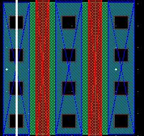
Delete the metal1 and contacts in the NMOS
Ground Pin
DRC
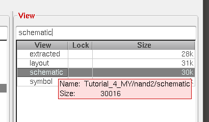
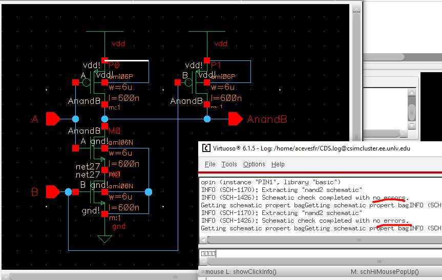
Extract the layout
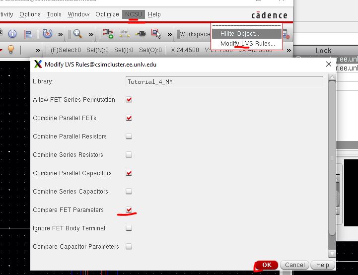
LVS
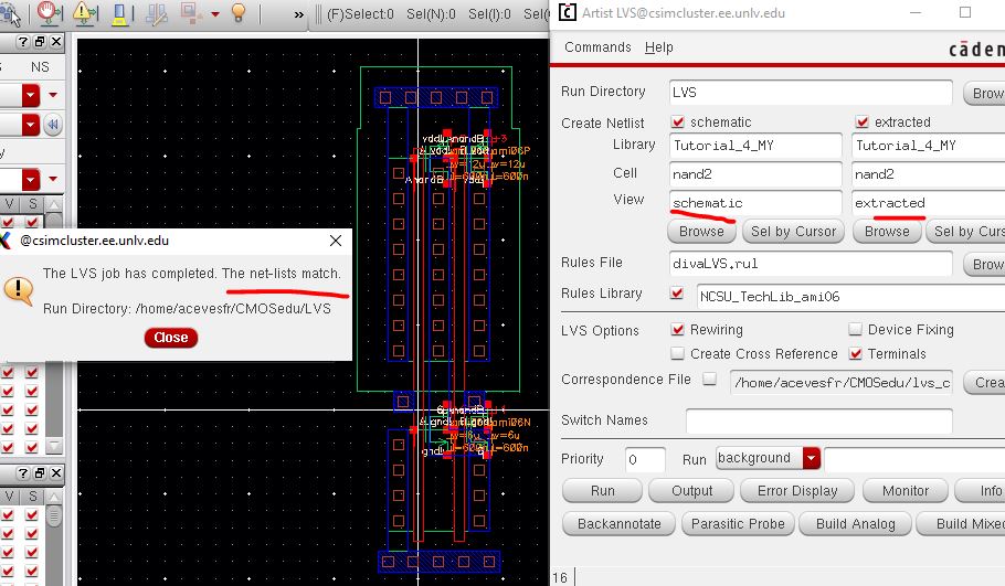
Knowing
that the PMOS in the schematic doesn’t match the layout we must change
the LVS rules by closing the LVS, and in the Extracted window, NCSU
-> Change LVS Rules
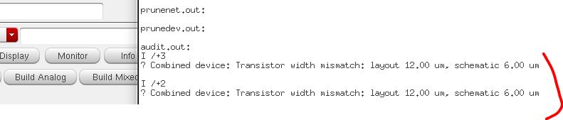
Rerunning the LVS gives us the following error but this is the end of the Prelab
END
************************************************************************************************************
Lab Work
- Draft
the schematics of a 2-input NAND gate (Fig. 12.1), and a 2-input XOR
gate (Fig. 12.18) using 6u/0.6u MOSFETs (both NMOS and PMOS)
- Using these gates, draft the schematic of the full adder seen below
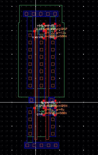
- Layout the full-adder by placing the 5 gates end-to-end so that vdd! and gnd! are routed
- Layout the full-adder by placing the 5 gates end-to-end so that vdd! and gnd! are routed
- full-adder inputs and outputs can be on metal2 but not metal3
- DRC and LVS your full adder design
- The cells used to generate the images used on this webpage are found in lab6.zip
***********************************************************************************************************
Experiment 1
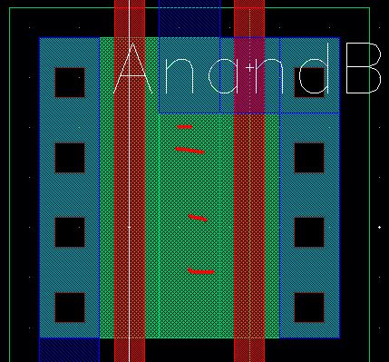
Creating the 2-Input NAND gate
schematic
Symbol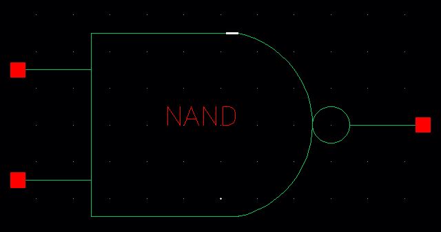
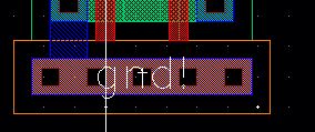
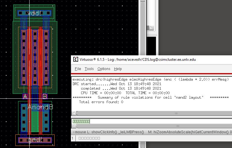
Layout and DRC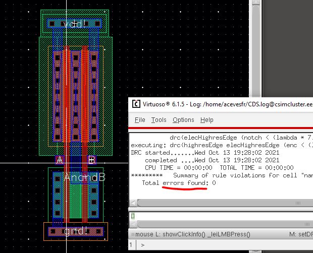
Extracted with LVS error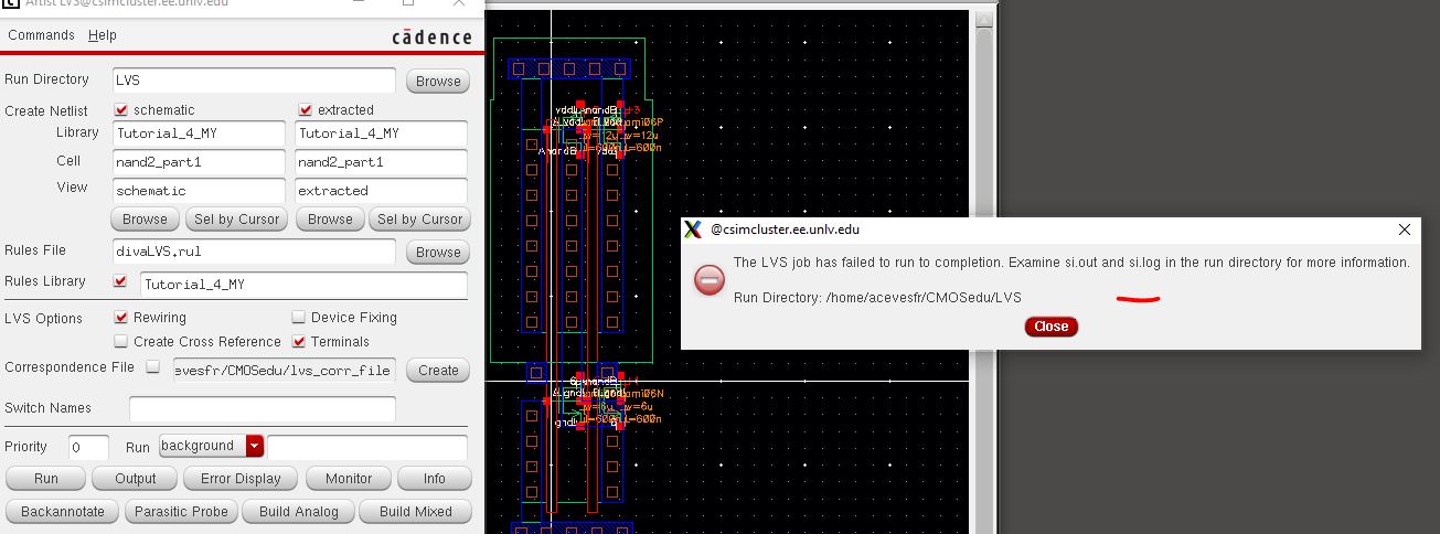
to fix the error we just change the size of the PMOS to a W=6μm.
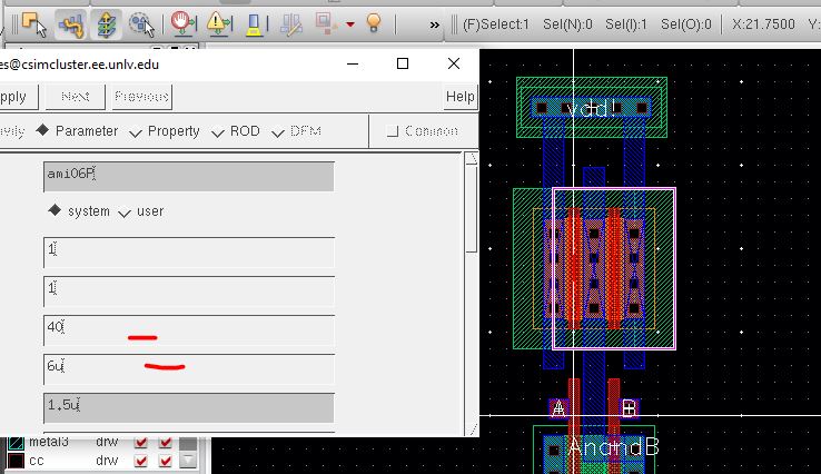
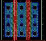
Resizing and moving a few layers and DRC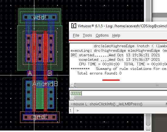
Extracting and LVS 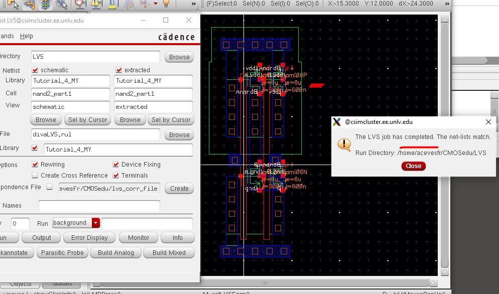
this
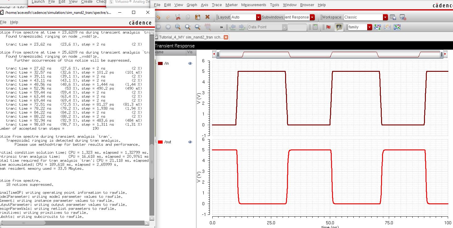
Simulation is basically showing that when one input is HIGH, that the
output will be logical LOW when Vin is HIGH and logical HIGH when Vin
is LOW (properties of NAND Gate). This is basically an Inverter, and can be useful later on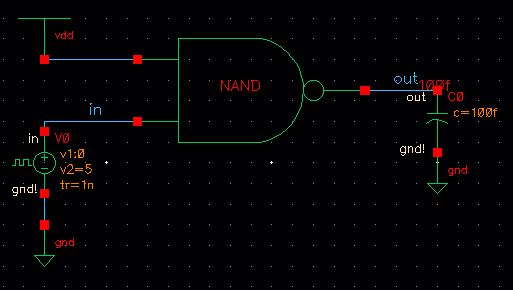
Transient 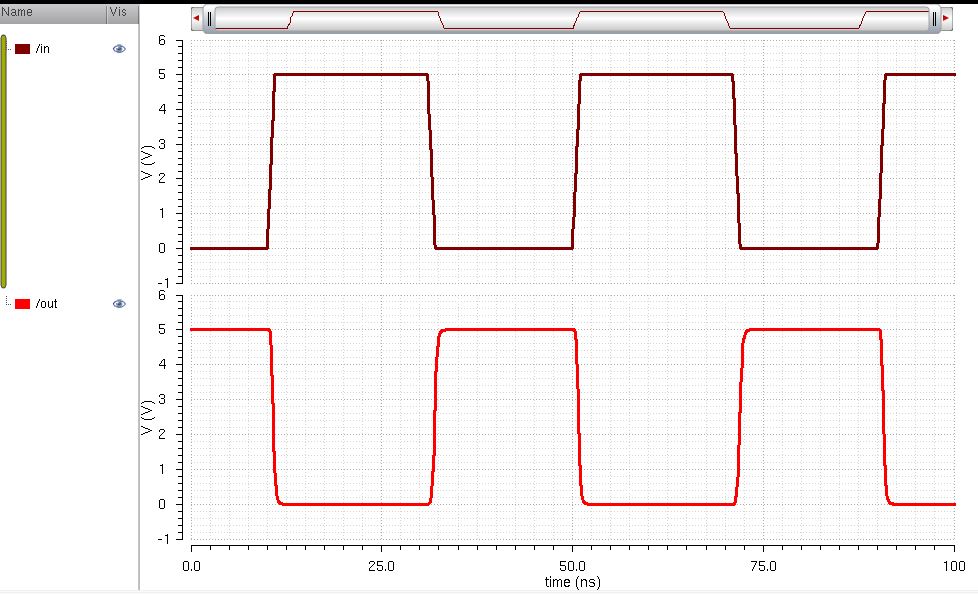
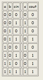
Truth Table of the NAND Gate
Input A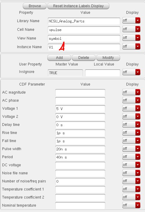
Input B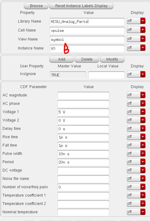
Output transient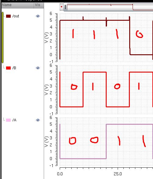
Using inerter Filters in sim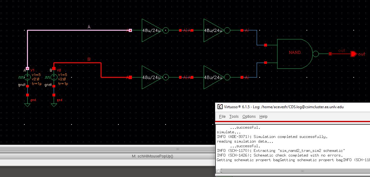
Output Transient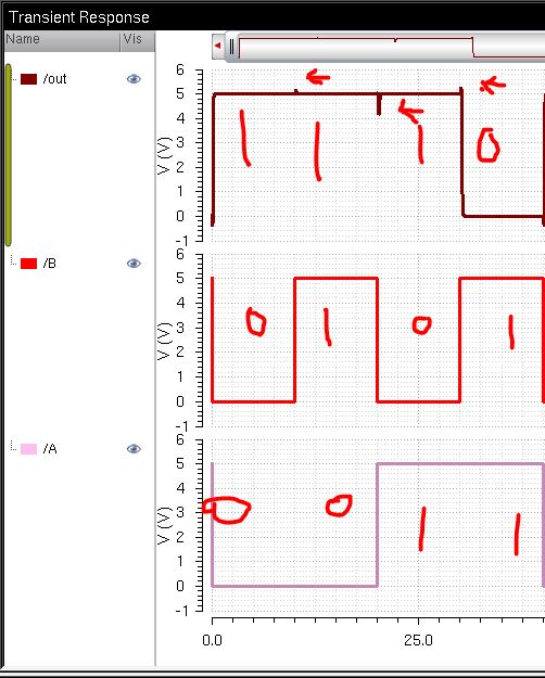
Experiment 2: Creating the 2-Input XOR Gate
schematic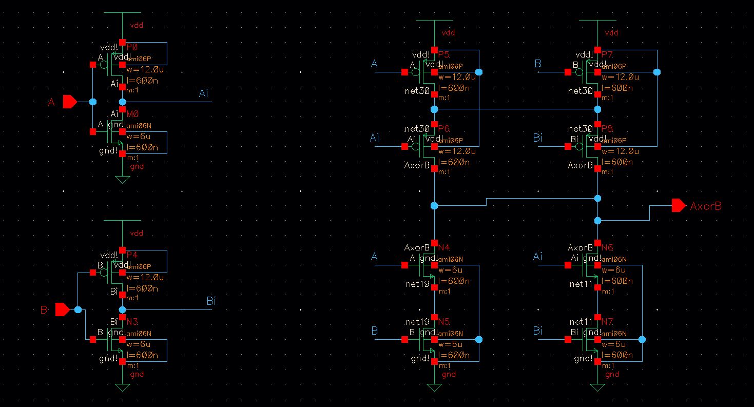
symbol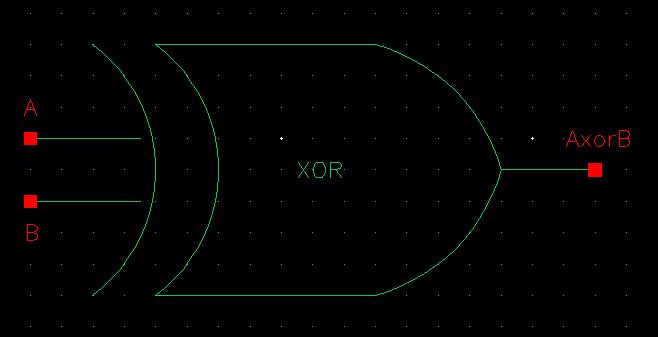
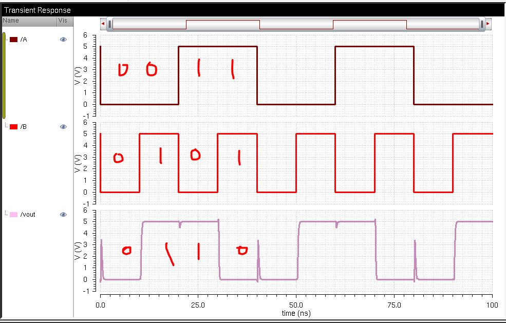
simuation setup with xor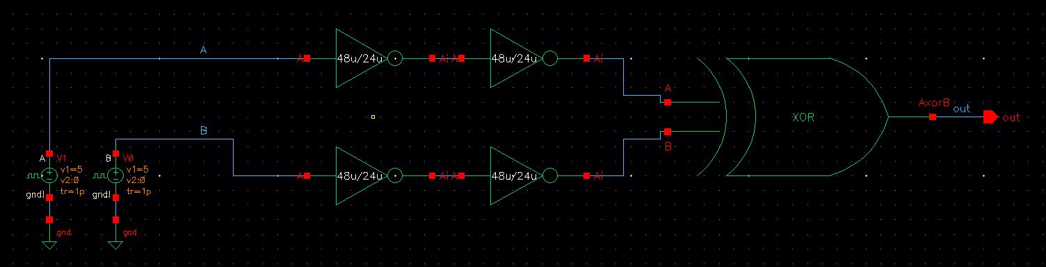
Output Transient
Layout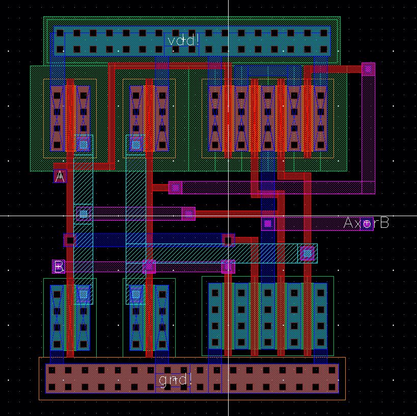
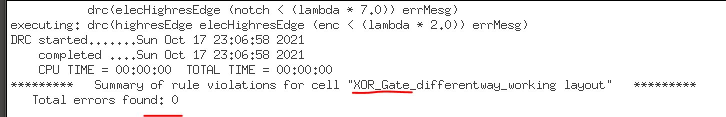
DRC
Extracted layout
LVS of layout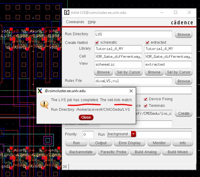
Ouput of LVS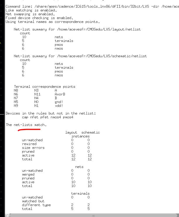
Experiment 3: The Full Adder
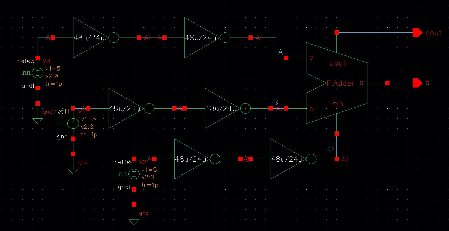
Creating a new schematic using the NAND and XOR gates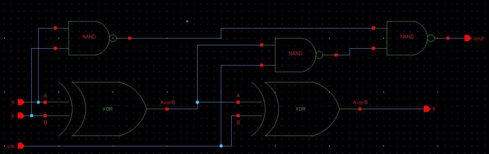
Symbol
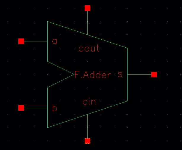
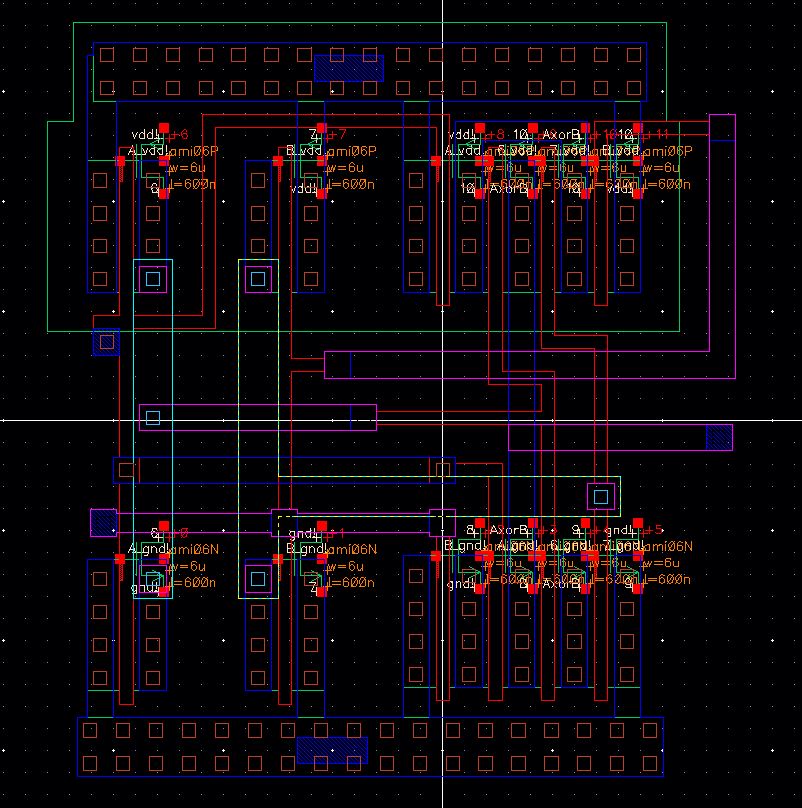
Layout of FULLAdder
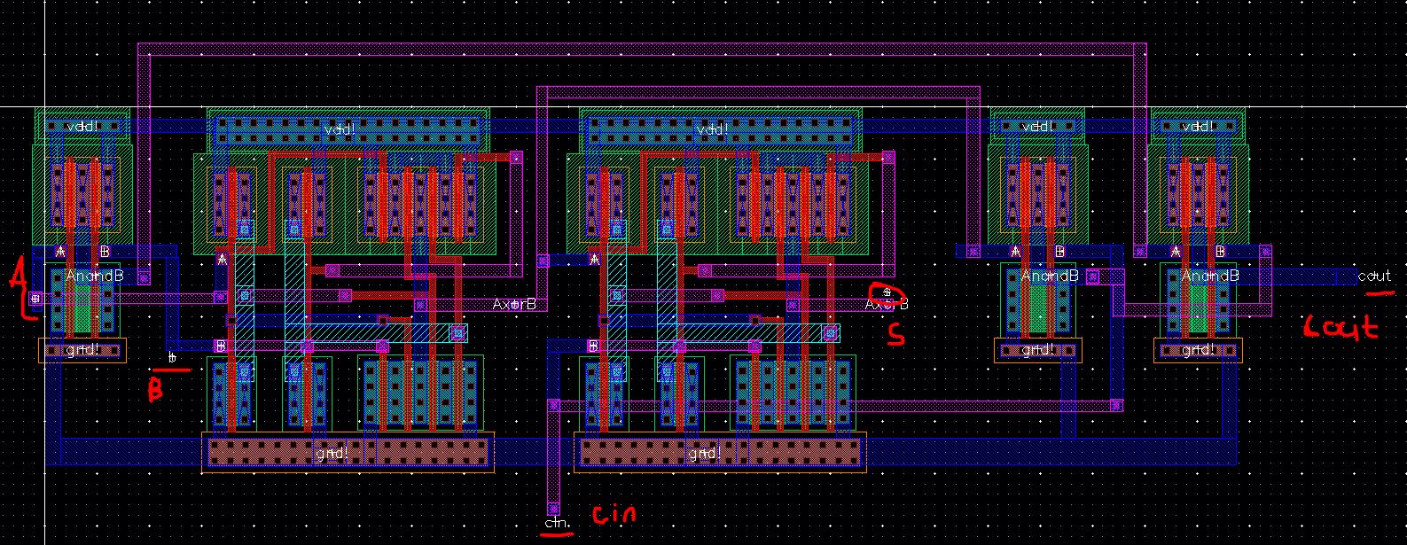
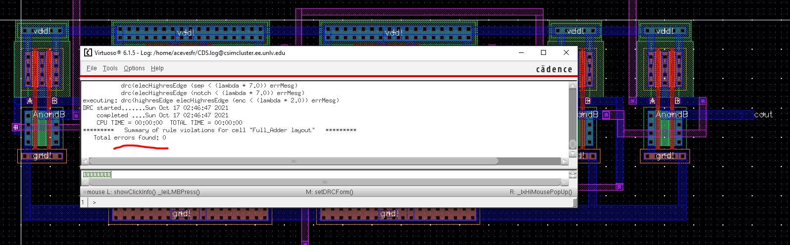
layout with DRC
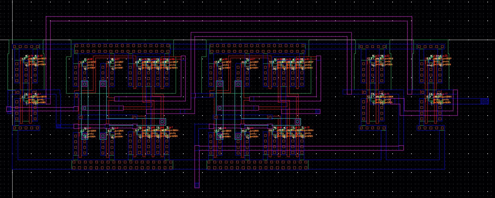
Extracted layout
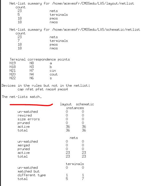
LVS
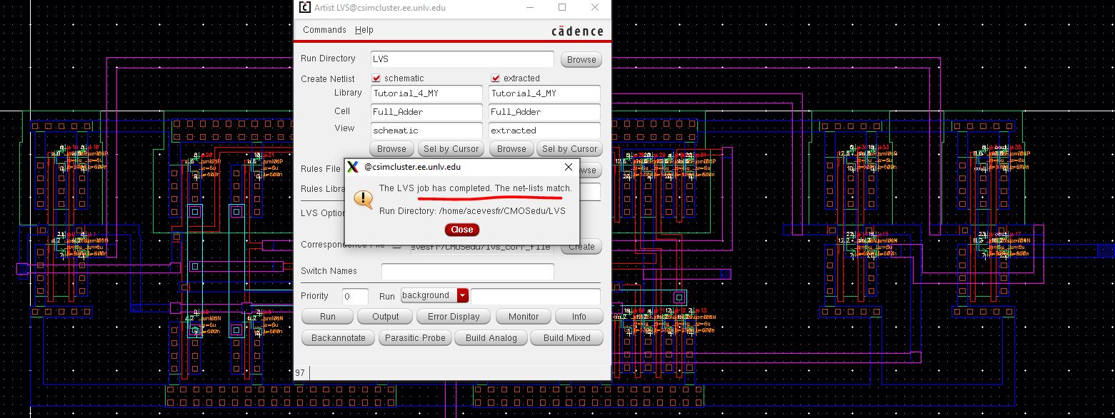
Output of LVS
Simulation setup of Full Adder
Output transient
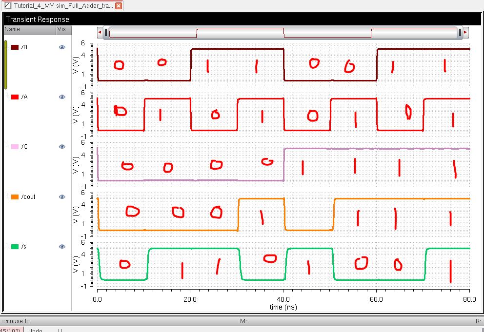
output transient matches this chart
END of Lab
Backing up my work
Return to Labs