Lab 5 - EE 421L
Damian Aceves-Franco
acevesfr@unlv.neveada.edu
9/22/2021
September 22 – Lab5 – Design, layout, and simulation of a CMOS inverter, due October 6
*****************************************************************************
Pre-lab work
- Back-up all of your work from the lab and the course.
- Go through Tutorial 3 seen here.
Make tutorial 3 from tutorial 2

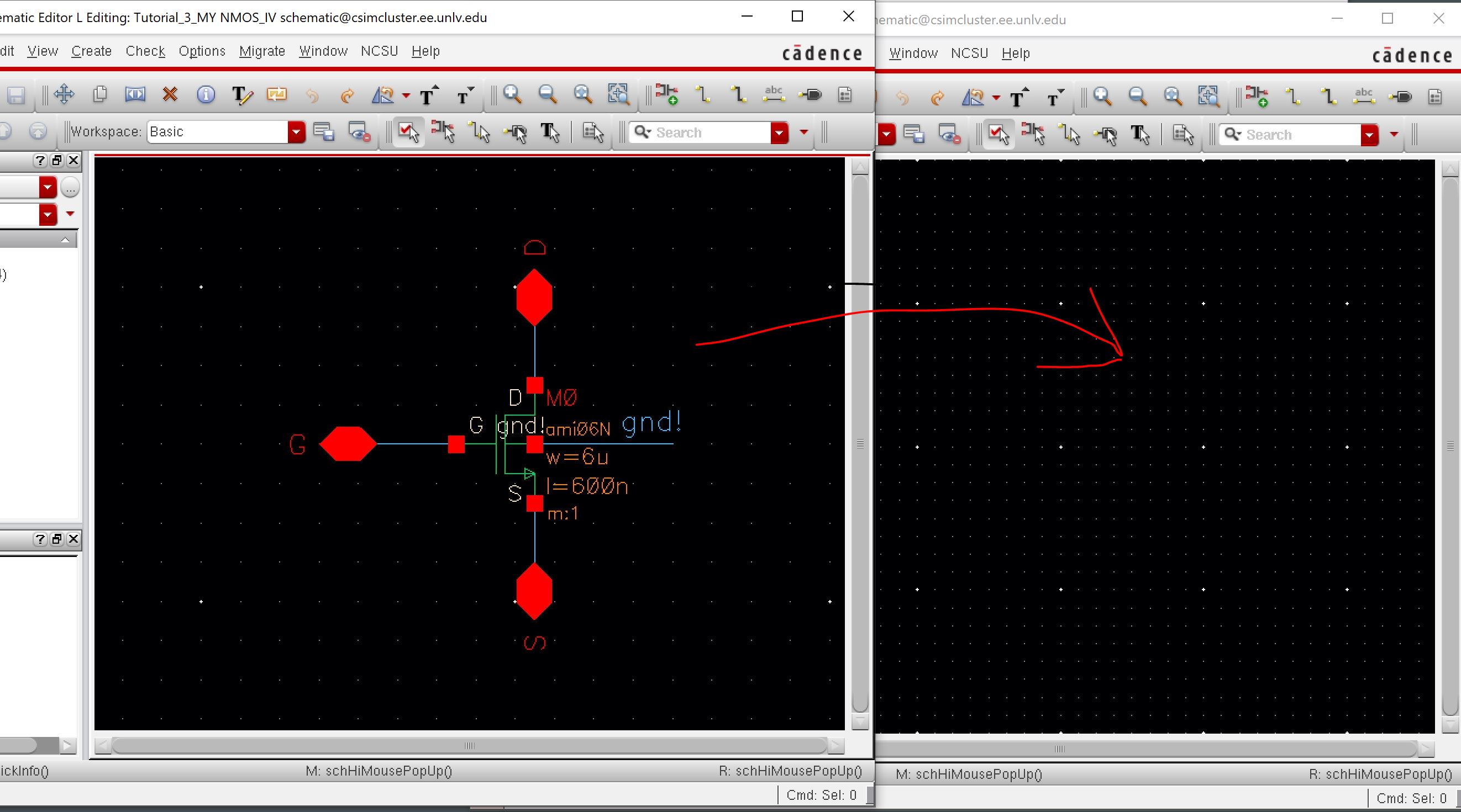
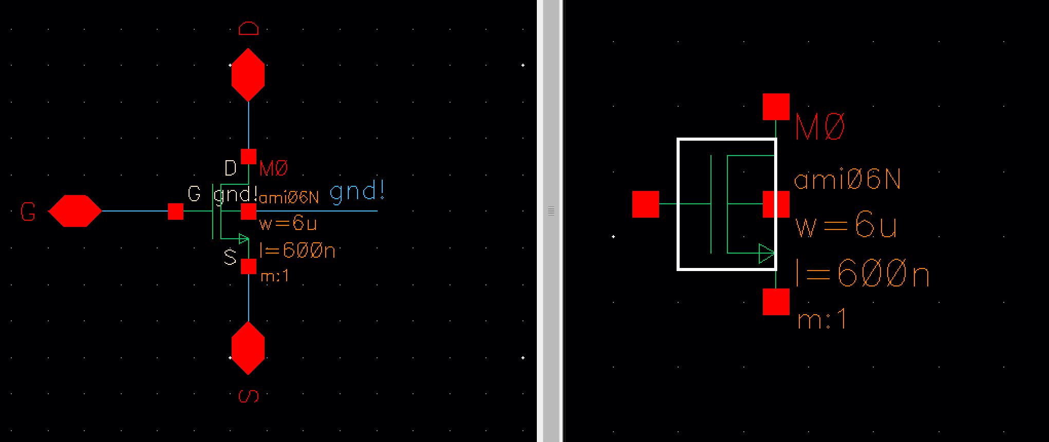
Creating a new schematic, “inverter”, and opening up NMOS_IV schematic, we will copy/paste the nmos4 instance to a new schematic
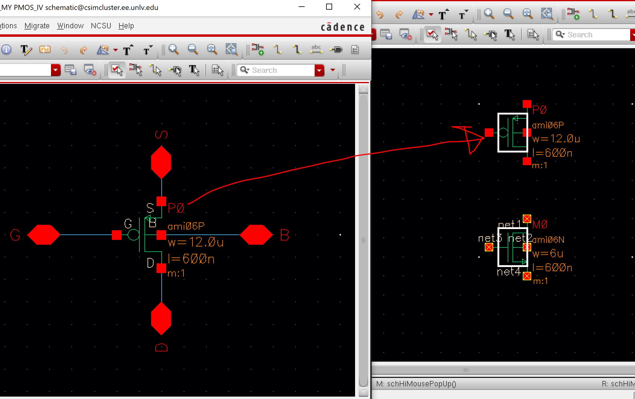
open PMOS_IV and do the same with pmos4
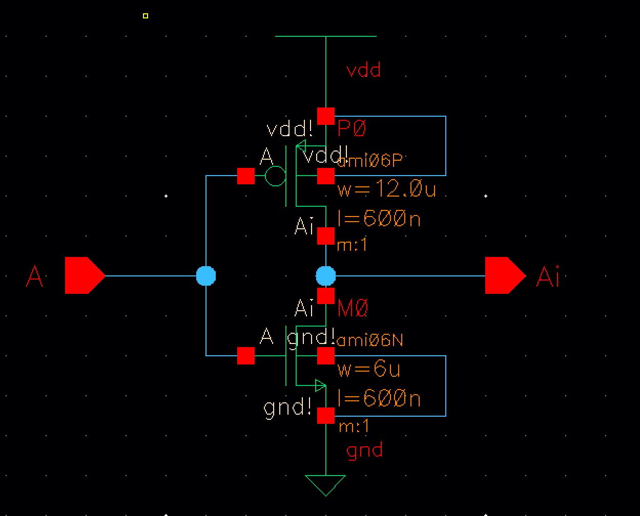
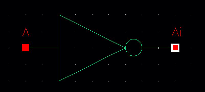
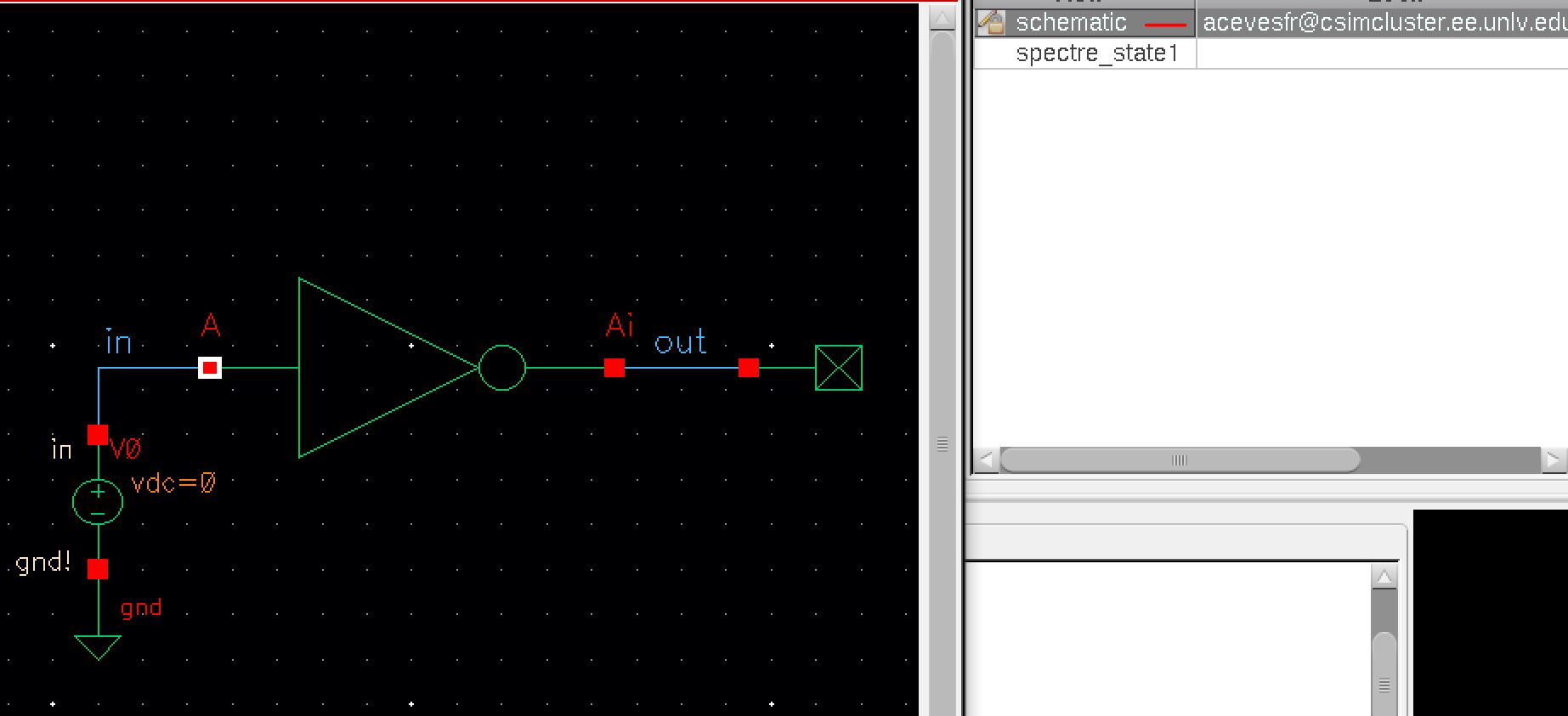
Wire the inverter, and add input pin A and output pin Ai
Creating symbol for this inverter to use in another schematic (Create -> Cell View -> From Cell View)
Create a new layout window for the Inverter schematic
Add a 6μ/.6μ NMOS, 12μ/.6μ PMOS, ntap , ptap , and m1_poly to the layout Add poly and m1 rectangles to connect everything
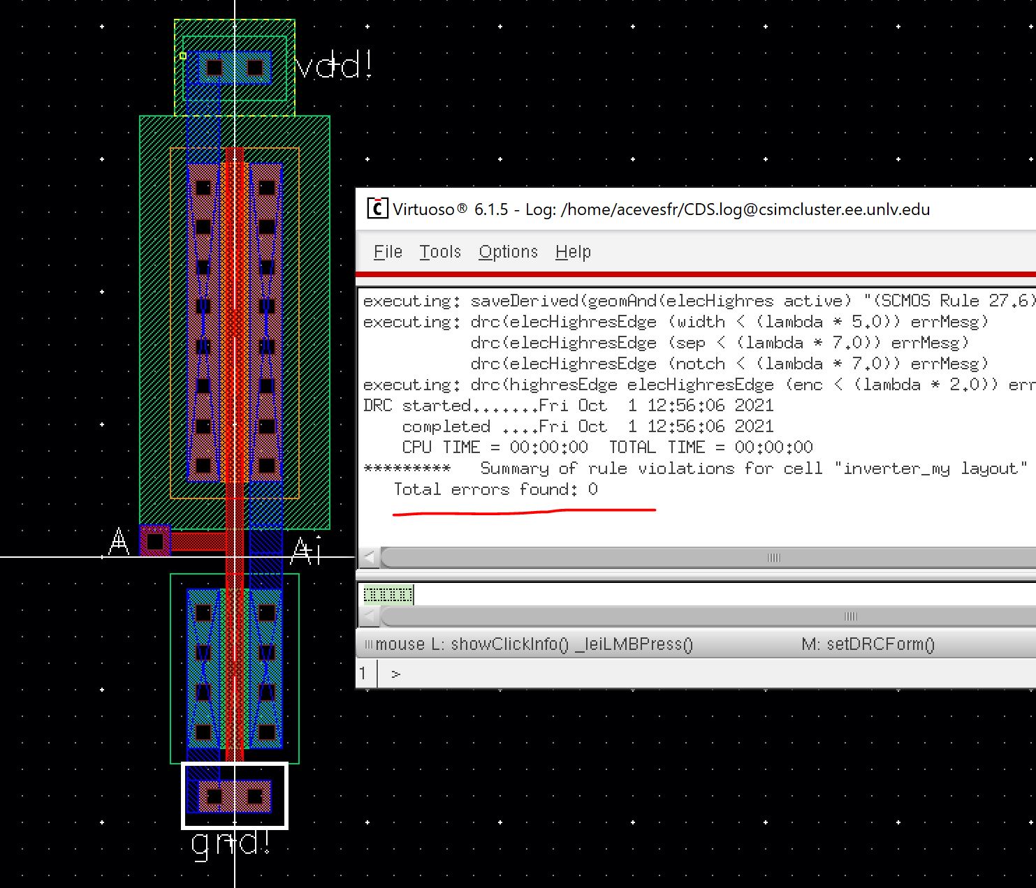
Add metal1 pins, where A is an input, Ai is an output. DRC the layout
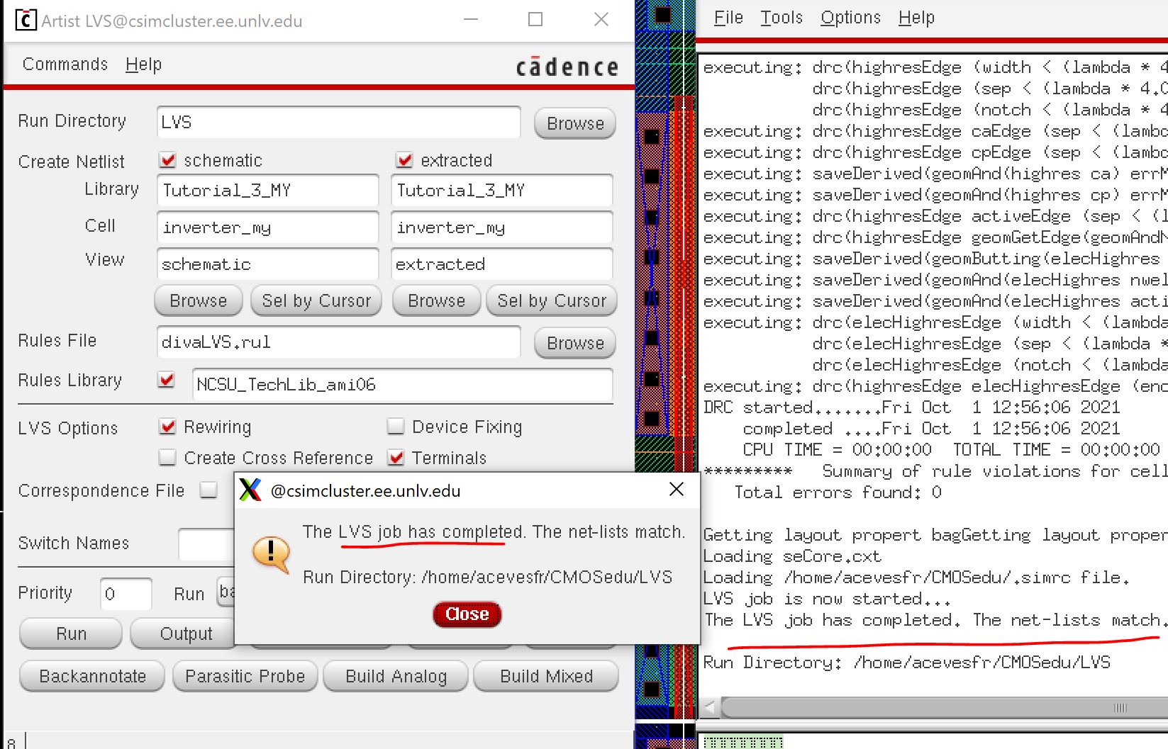
Extract the layout, and LVS the extracted layout
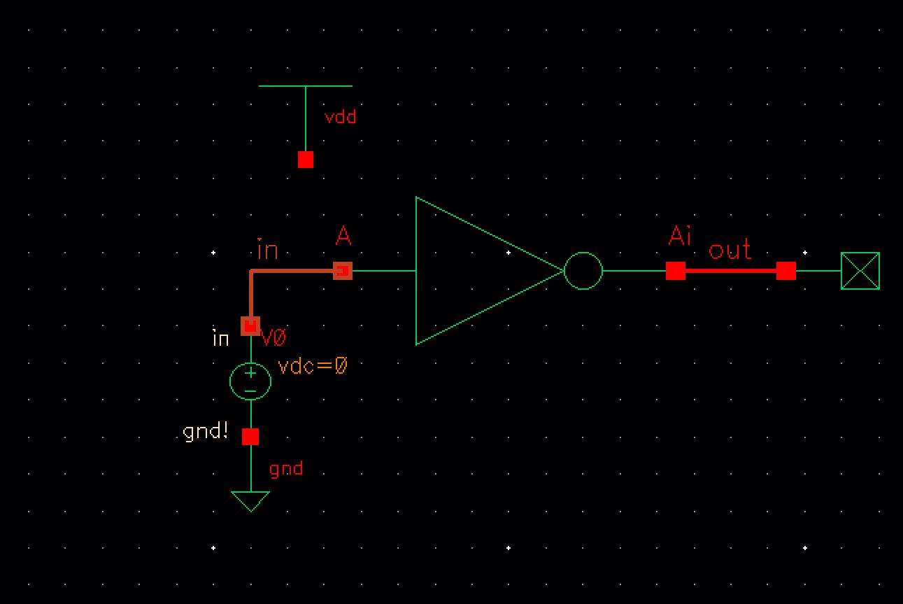
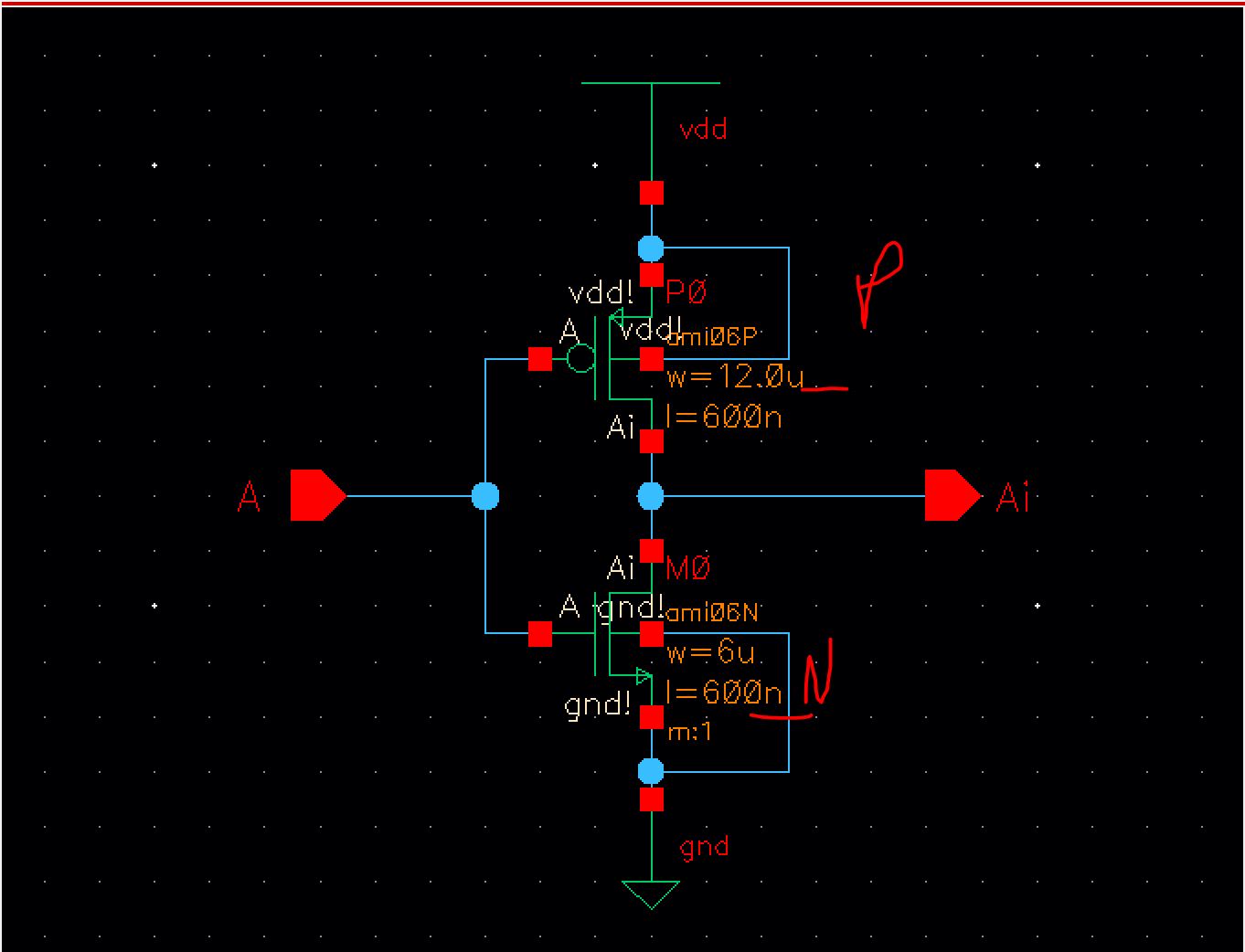
Make a new schematic and create the following schematic
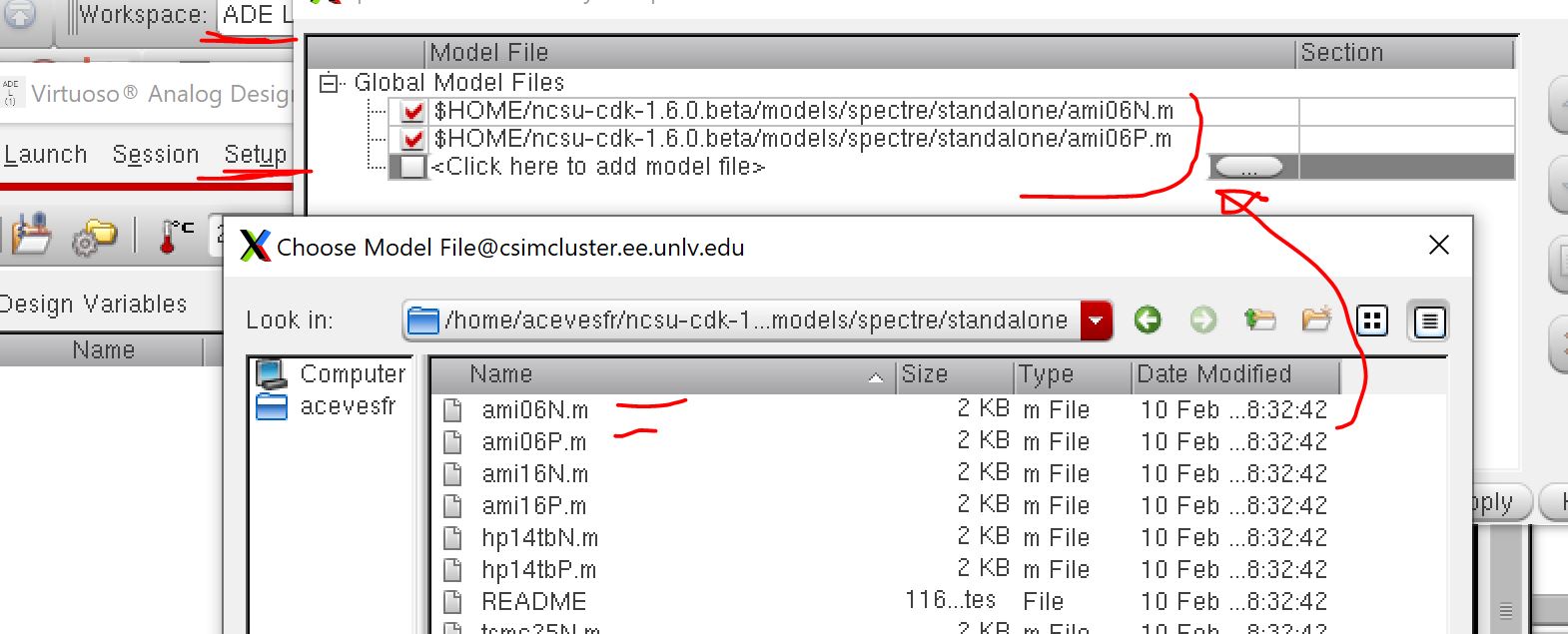
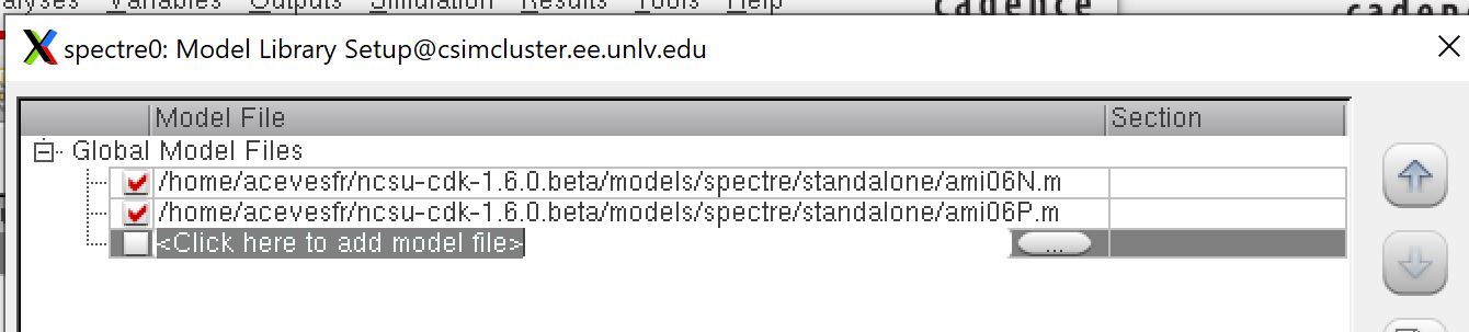
Launching the ADE, and setting up the MOSFET models
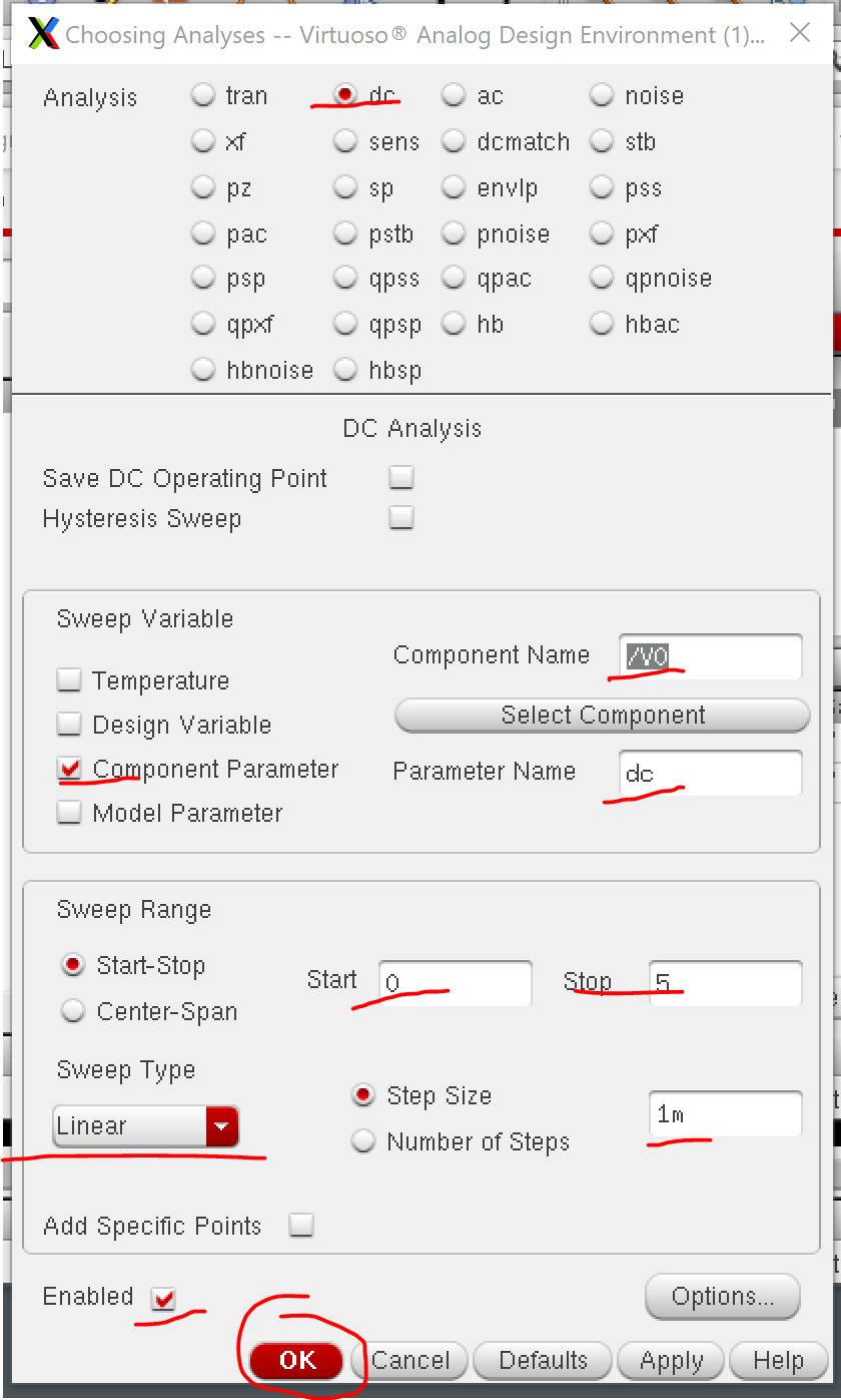
go to choosing analyses and to the following
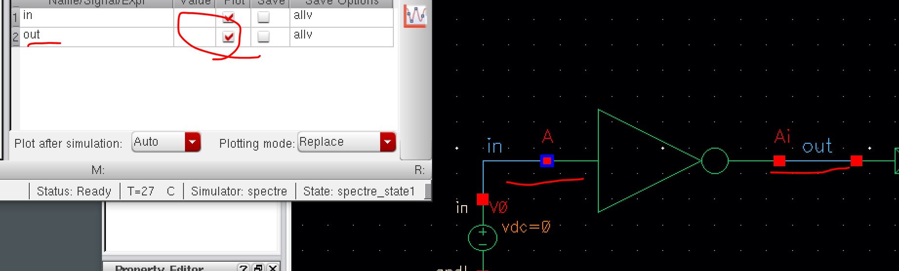
choose your outputs
Using Graph -> Split Current Strip to see the 2 signals in 2 different graphs
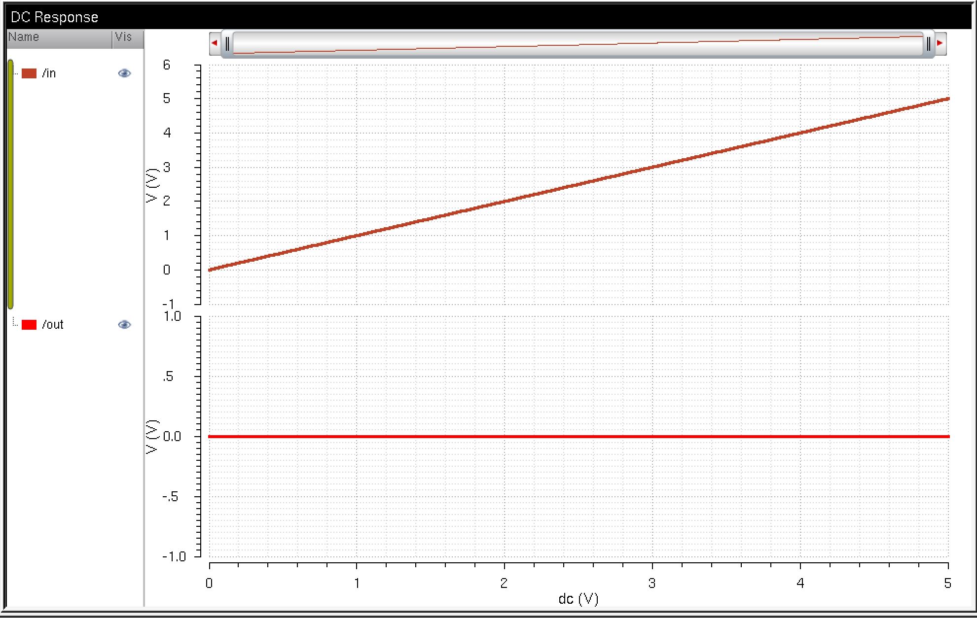
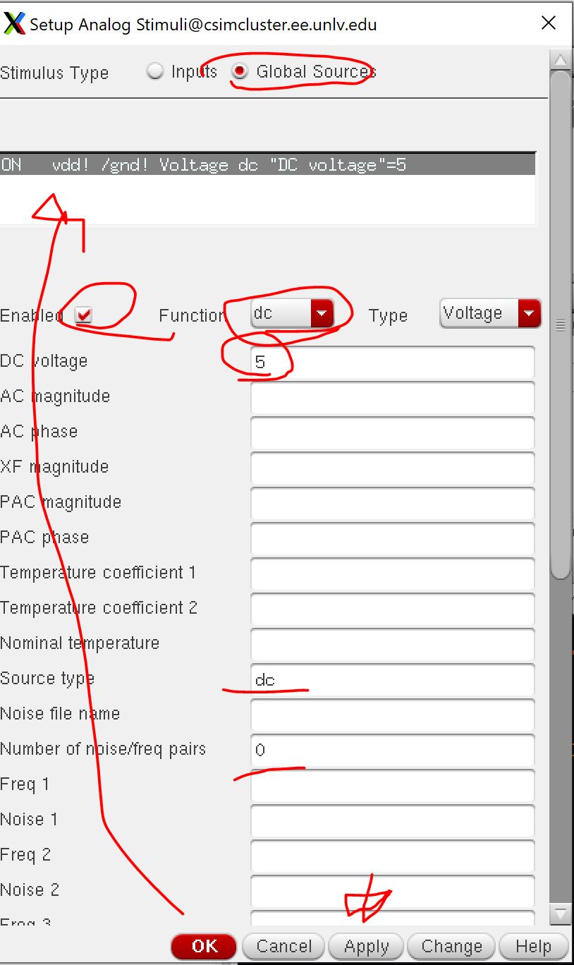
Adding a vdd! because There is no output due to there not being a “vdd!” source. Instance to the schematic and also setting it in the ADE Setup -> Stimuli
Rerunning the Simulator using the saved states
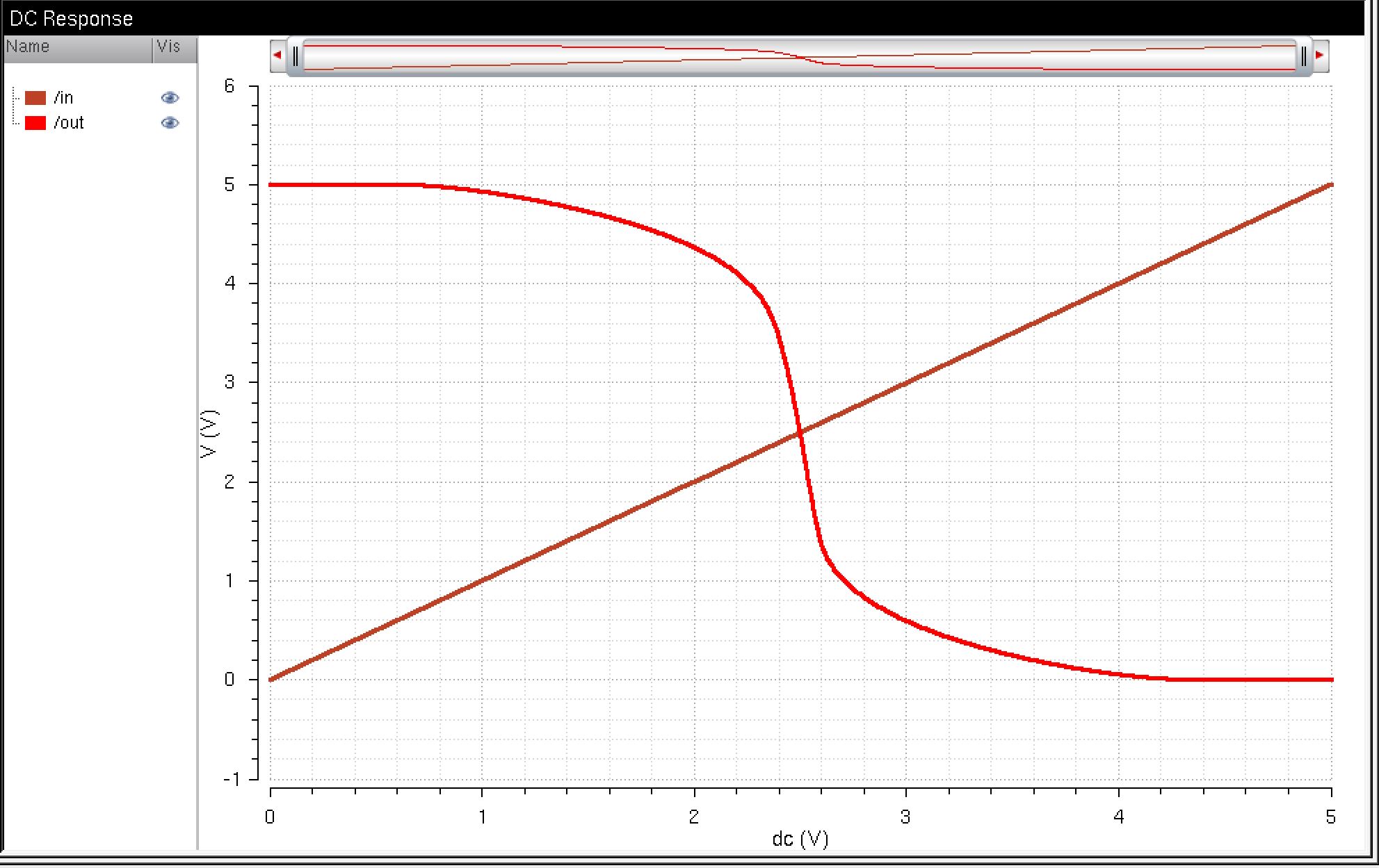
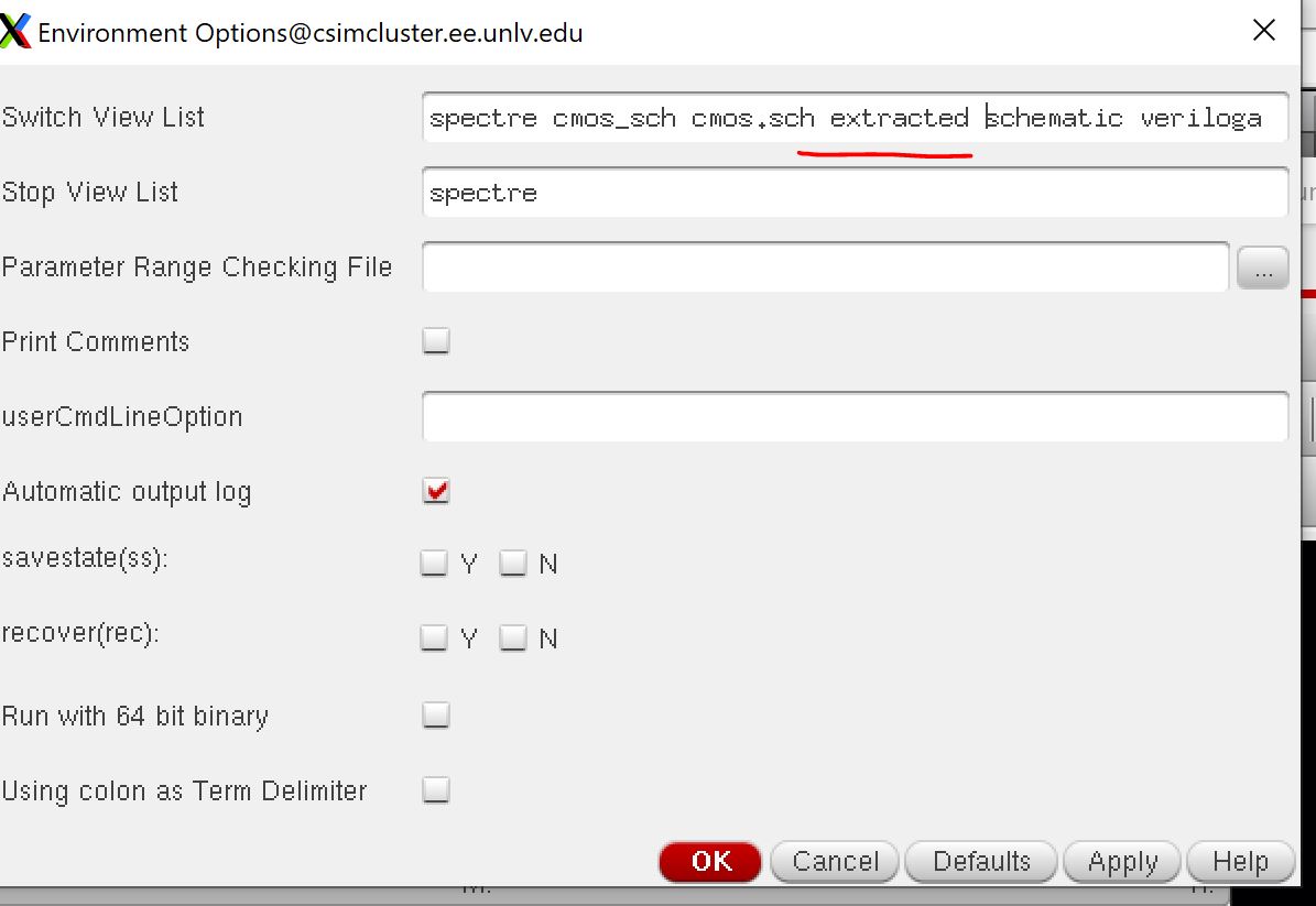
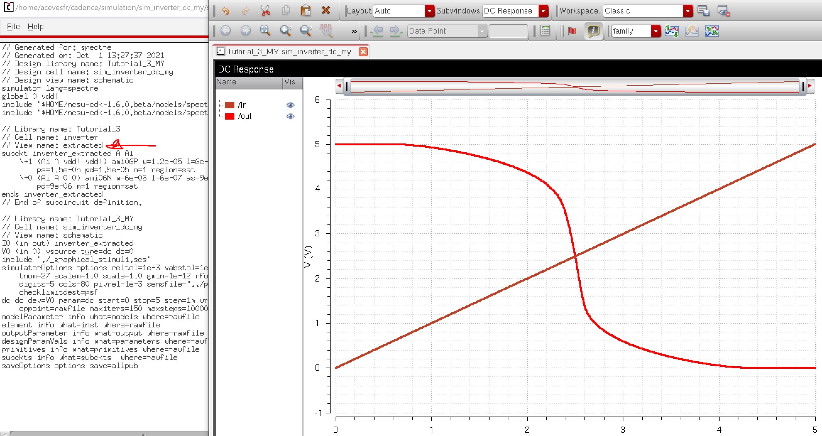
Now simulate the Extracted Layout and do the following and add extracted in the statement Using ADE Setup-> Enironment
END of Prelab
***************************************************************************************
Lab work
- Draft schematics, layouts, and symbols for two inverters having sizes of:
- 12u/6u (= width of the PMOS / width of the NMOS with both devices having minimum lengths of 0.6u)
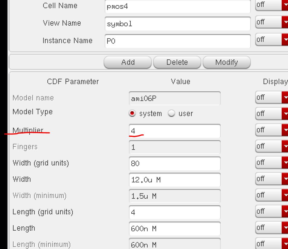
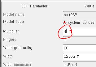
- 48u/24u where the devices use a multiplier, M = 4 (set along with the width and length of the MOSFET, image), as seen below
- Using SPICE simulate the operation of both of your inverters showing each driving a 100 fF, 1 pF, 10 pF, and 100 pF capacitive load
- Comment, in your report, on the results
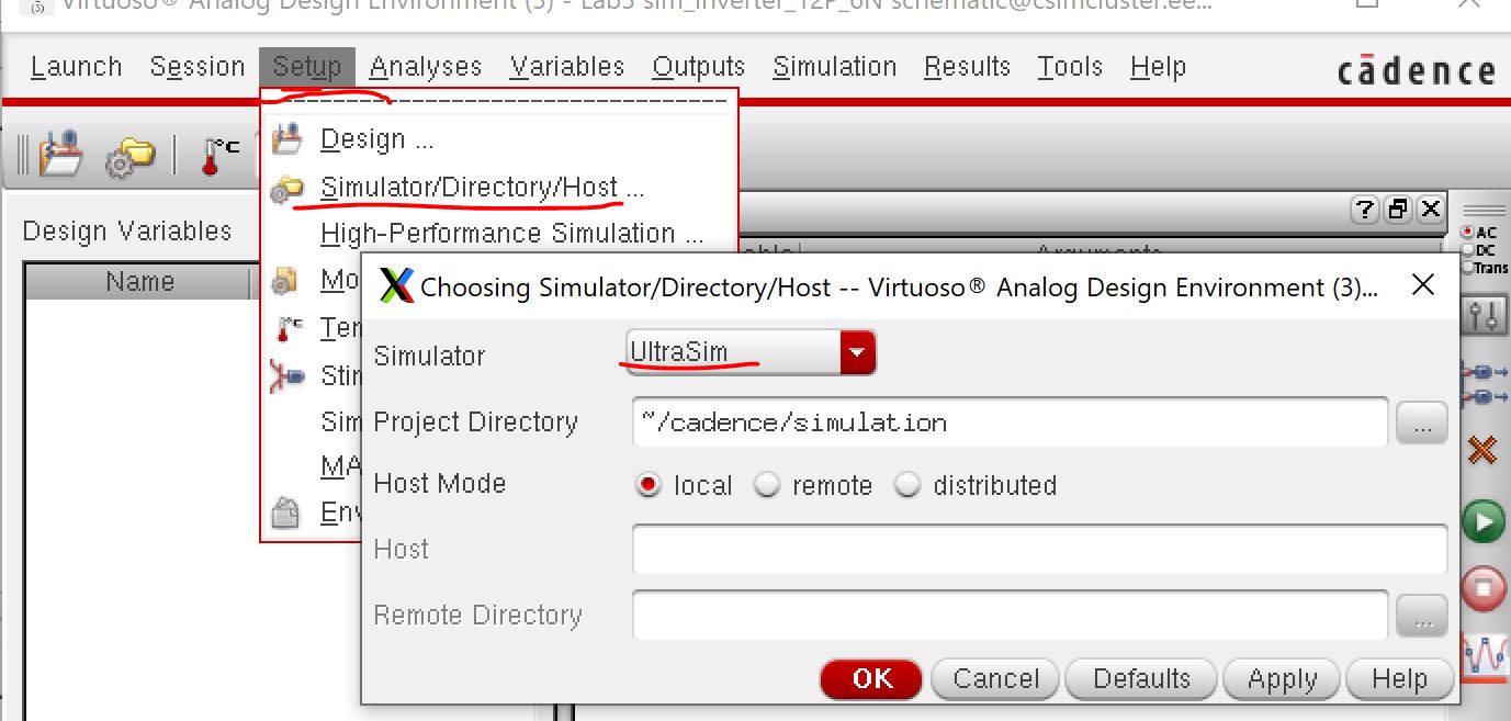
- Use UltraSim (Cadence's fast SPICE simulator for larger circuits at the cost of accuracy) and repeat the above simulations
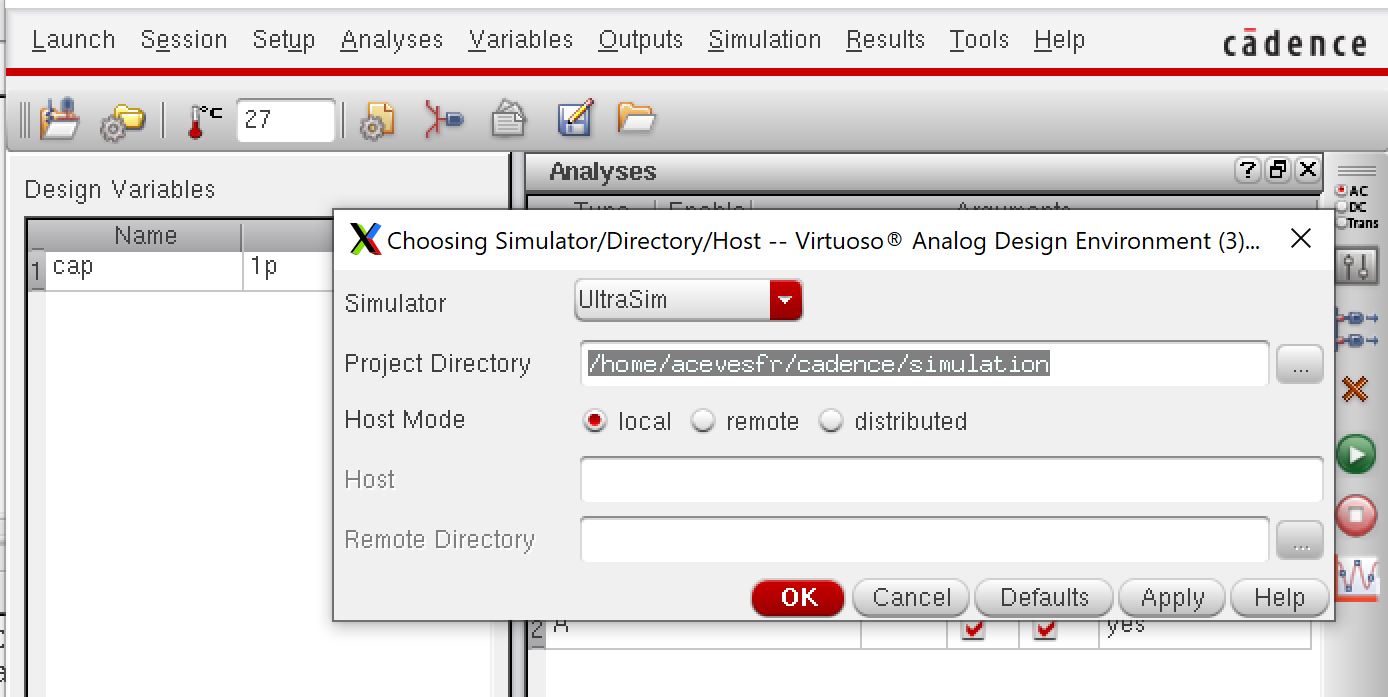
- Use Setup -> Simulator/Directory/Host and select UltraSim as seen below
- You'll also have to point to the MOSFET models again as seen below
- Note that UltraSim only performs transient simulations (not AC, Noise, DC, operating point, etc.)
- Not knowing this last item will lead to wasted time if trying to use UltraSim exclusively for simulations
***************************************************************************************
Lab
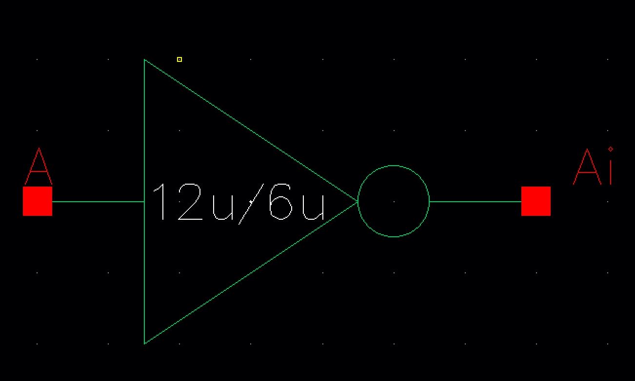
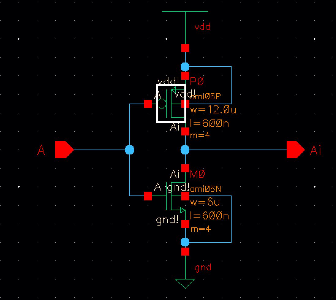
Experiment 1: Schematic, Layout, and Symbol for a 12μ/0.6μ PMOS and 6μ/0.6μ NMOS
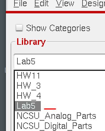
Make new Libary->Lab5
Schematic of the 12/6 PMOS-NMOS inverter
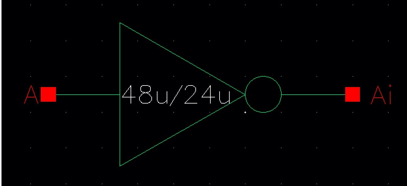
Create symbol for this inverter Create -> Cell View -> From Cell View
Layout the Inverter and DRC
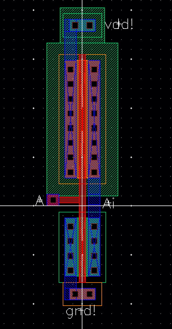
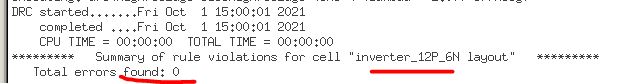
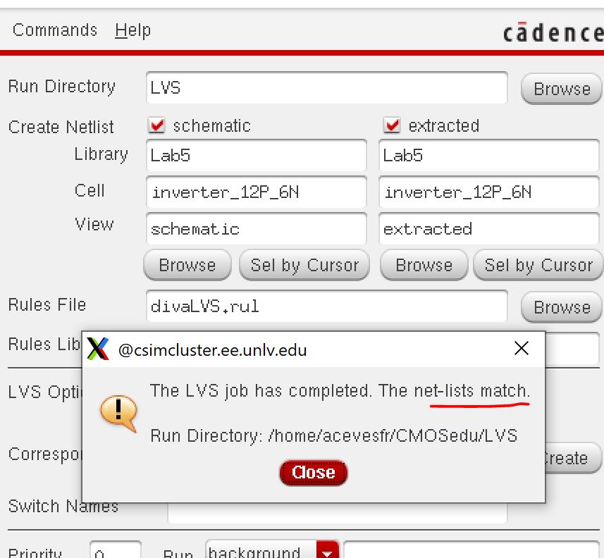
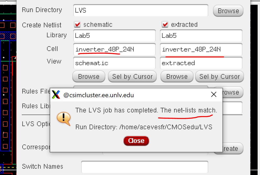
Extract the layout, and LVS the extracted layout
Experiment 2: Schematic, Layout, and Symbol for a 48μ/0.6μ PMOS and 24μ/0.6μ NMOS by the use of
Mulitplier in CDF parameters with value 4
Copy experiment 1 cell and change the CDF parameters of PMOS and NMOS
layout the schematic
make a symbol
Layout the Inverter in layout and DRC then extarct it
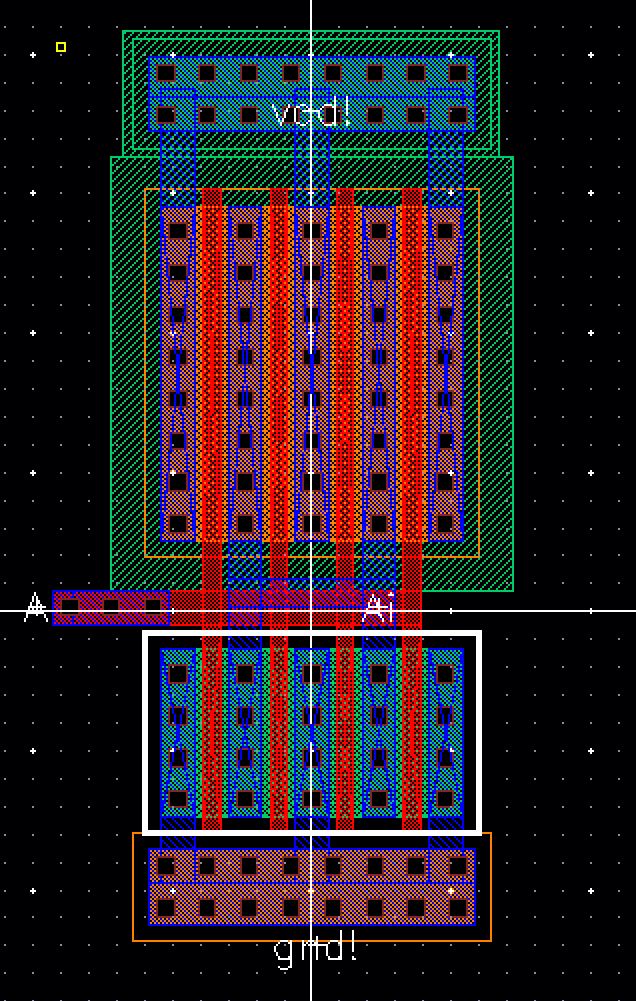
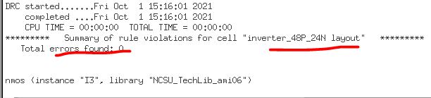
Do the LVS
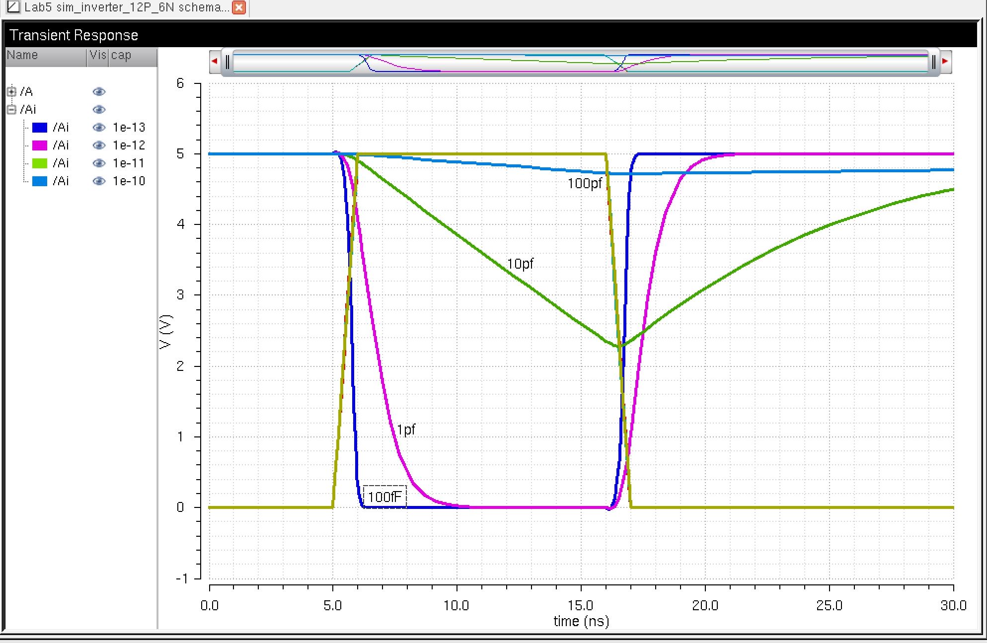
Experiment 3: Simulations of 12μ/6μ inverter
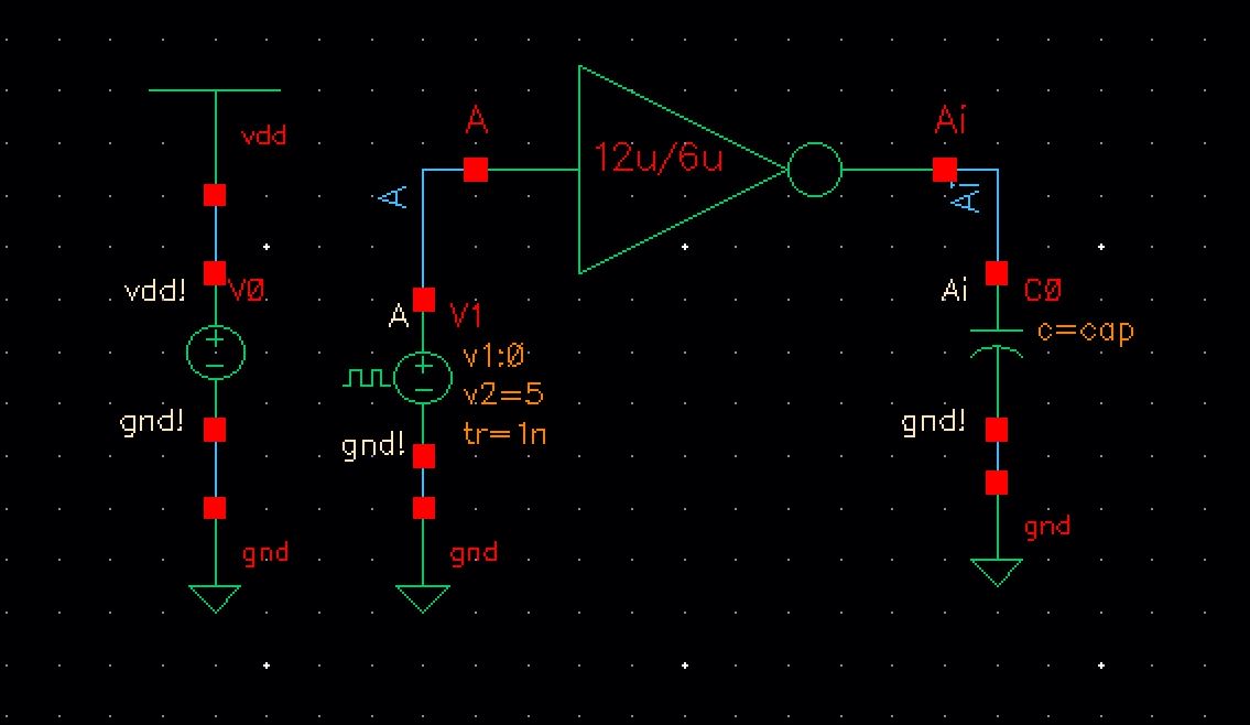
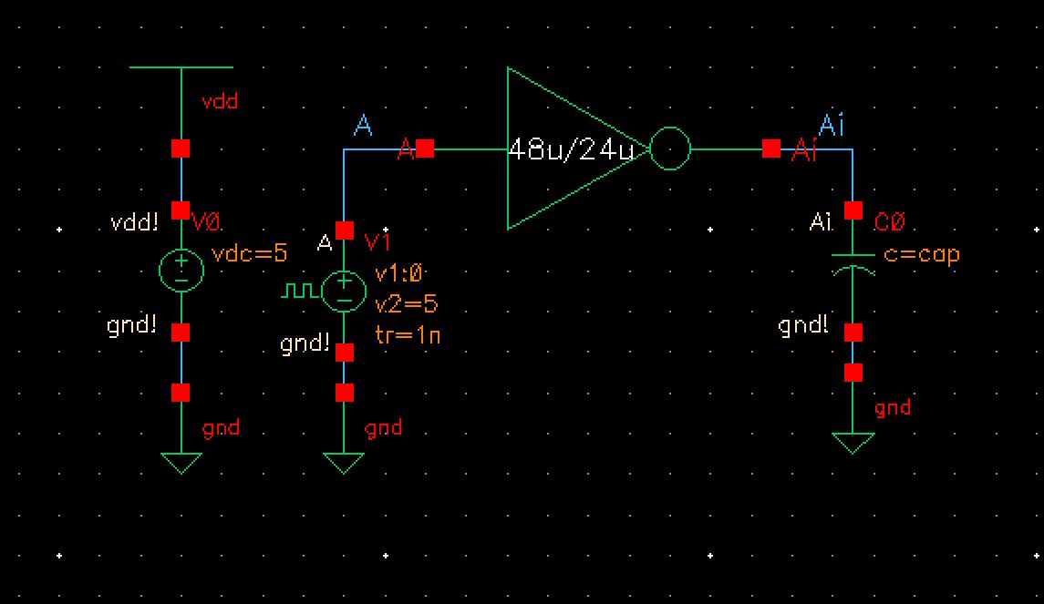
Simulating the 12μ/6μ Inverter first, here is the following schematic
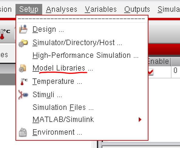
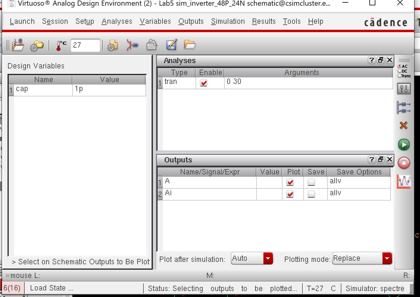
Launching the ADE, adding the model libraries, and doing a transient response
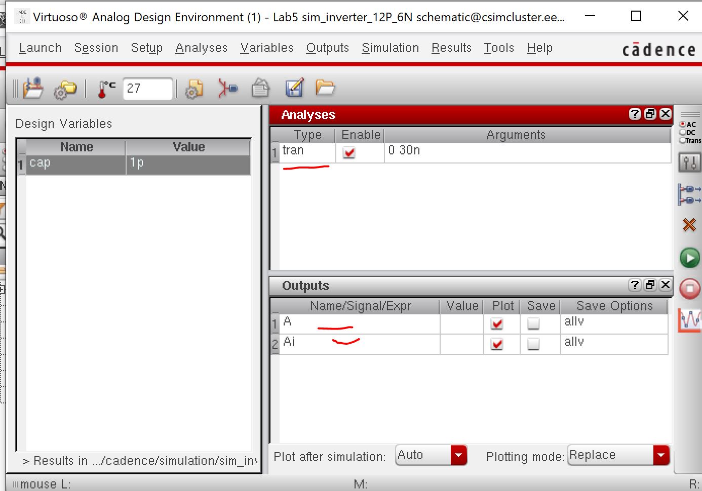
make sure to do the following and to add the variables
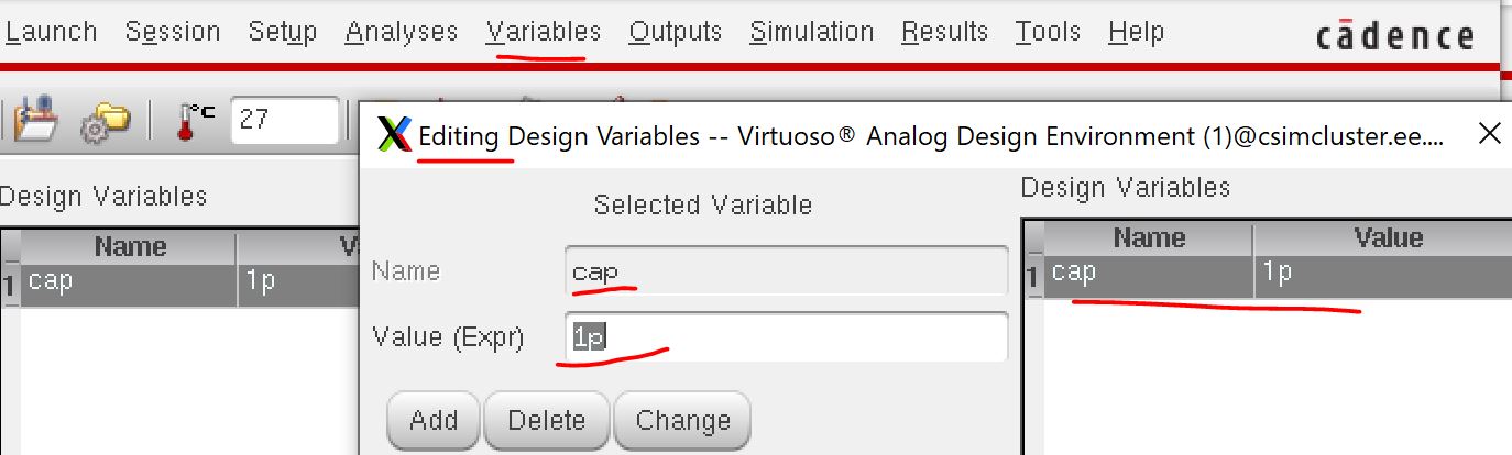
load Model Libraries
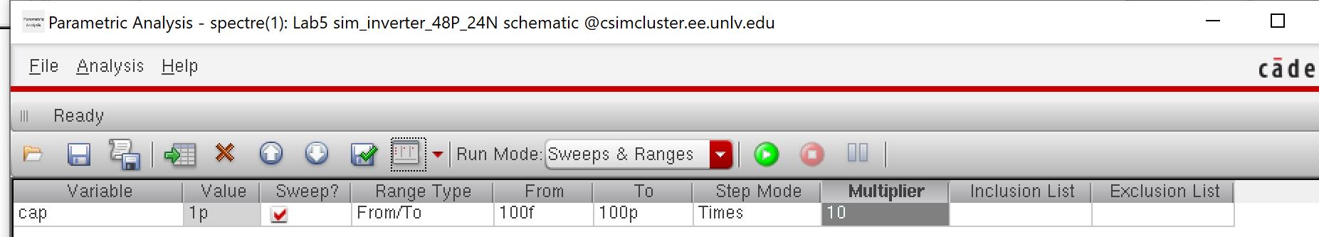
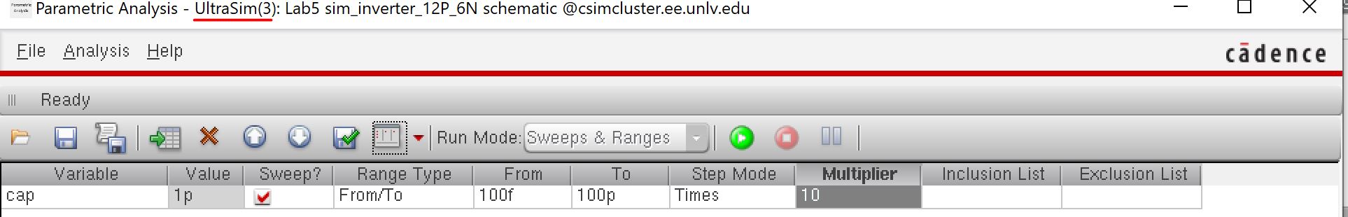
open Parametric Analysis with the Variable cap and input the following information
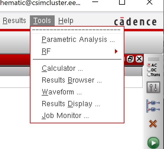
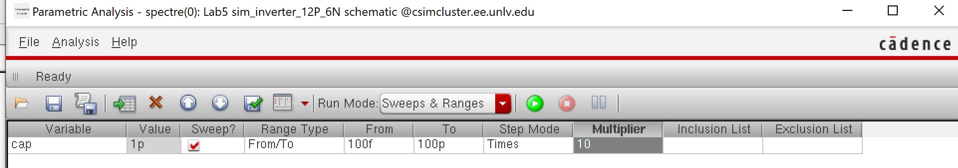
press the green button
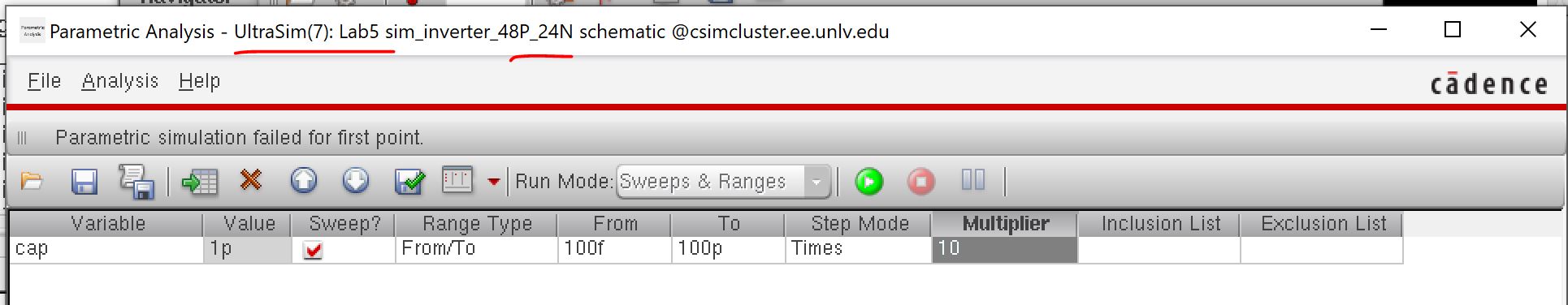
Simulating the 48μ/24μ Inverter the same way we did the 12/6 Inverter
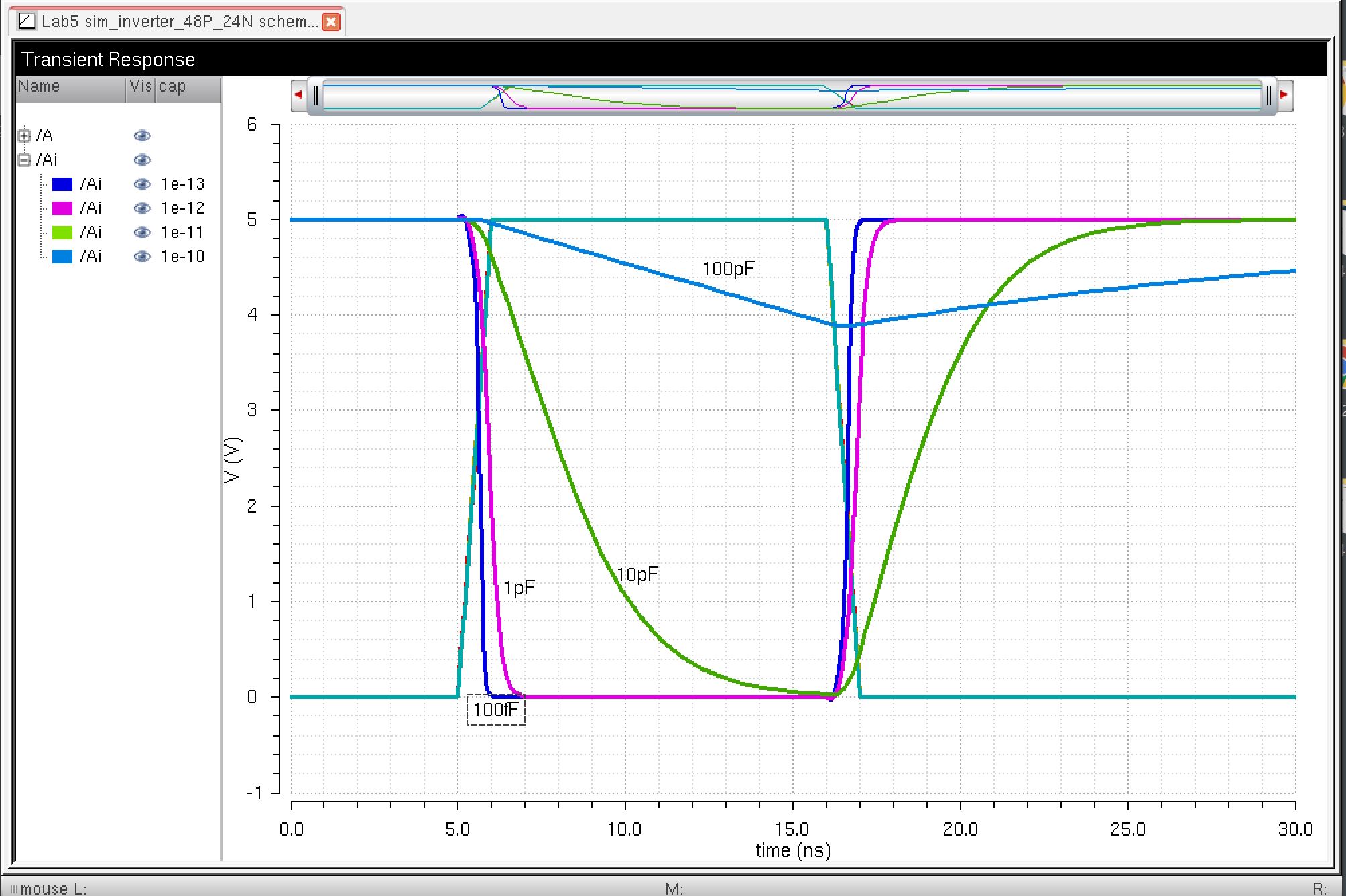
Higher capacitances make the inverter have faster fall times. And bigger MOSFETs also give faster fall times and high gains.
Experiment 4: Simulations with Ultrasim
Setup the following for ultrasim
Press OK
Set the Parametric analysis again and Run (Green Button)
Doing the same for the 48u/24u Inverter
End of Lab
*******************************************************************************************************************
files used in this lab can be downloaded HERE
and lastly I must backup my work
Return to Labs