Lab 4 - ECE 421L 


Authored by Do Le (led2@unlv.nevada.edu)

16th of September, 2020


Lab Description

    The purpose of this lab is to analyze the I-V curves of the MOSFET devices. This includes the NMOS and PMOS transistors.
    The I-V curves of the MOSFET is a three terminal device commonly used as a switch of amplifier; the terminals are labeled
    gate, drain, and source. The I-V curves of the device (the current flows between drain and source) is determined by the voltage
    between drain and source, as well as determined by the voltage between the gate and the source.
 
    To analyze the operations of the MOSFET, a schematic is used and the curves are graphed in simulation.
 
    Additionally, we will create layouts for the NMOS and PMOS devices.


Prelab

    To prepare for the lab, we finished tutorial 2 found here on the CMOSedu website.
    The tutorial explains how to create a MOSFET layout, and how to perform the simulations for the lab.


Lab

Simulating the IV Operation:

    During the first part of the lab, we simulated the I-V curves of the MOSFETs.


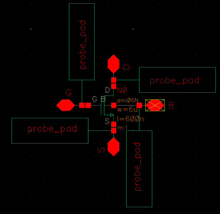
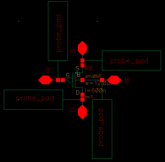
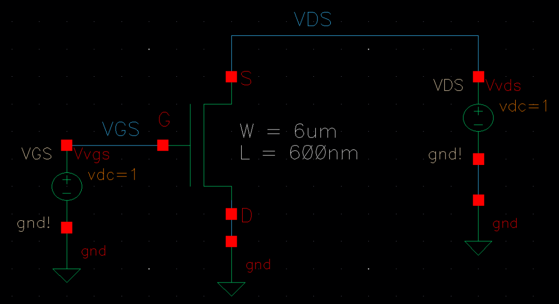
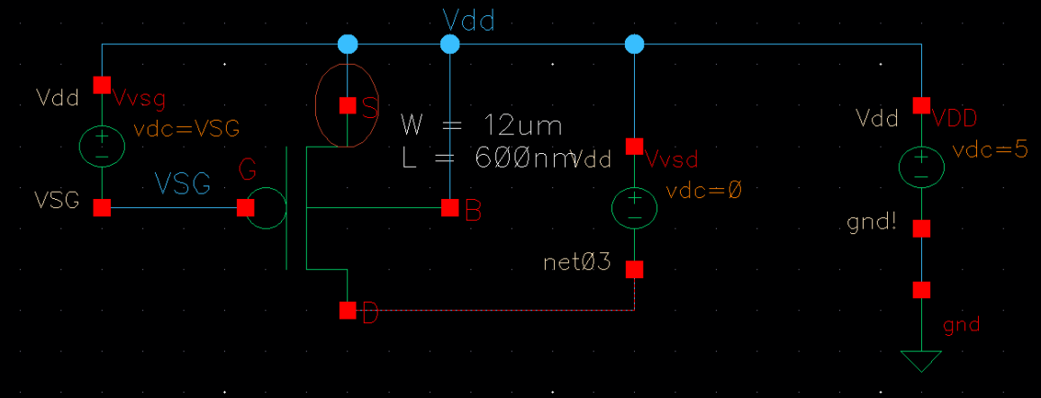
    We used the nmos and pmos available under the NCSU_Analog_Parts library. The NMOS used for simulation

    has a width of 6µm and a length of 600nm. The PMOS used for simulation has a width of 12µm and a length

    of 600nm.


    To simulate our transistors, a circuit is built to set the drain-to-source/source-to-drain voltages and the

    gate-to-source/source-to-gate voltages. The circuit is made as followed:

    For NMOS:

NMOS_IV_Schematic

    For PMOS:

PMOS_IV_Schematic


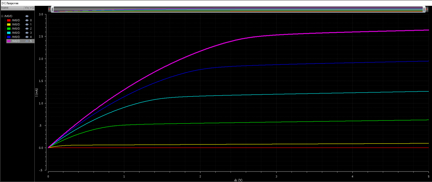
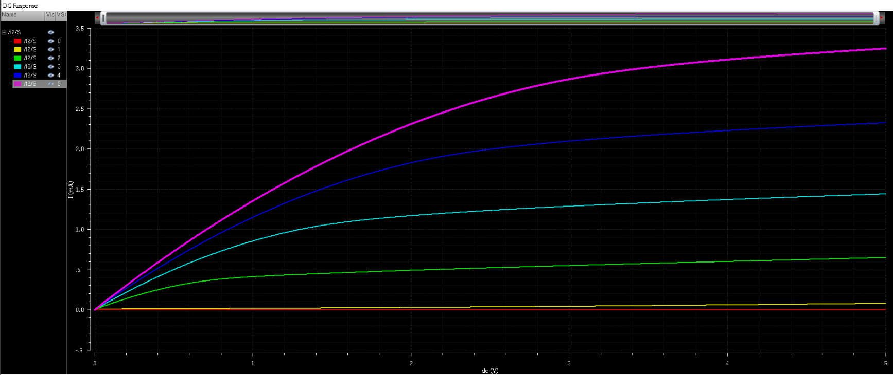
     Now we simulate the drain-to-source current for the NMOS and the source-to-drain current for the PMOS.

    We first start by simulating the currents by sweeping Vds for the NMOS and Vsd for the PMOS, effectively graphing

    Ids/Isd versus Vds/Vsd. This is done from 0V to 5V in 1mV increments, and is done for six different Vgs/Vsg values

    (0V, 1V, 2V, 3V, 4V, 5V, & 6V). The results are shown below.

    For NMOS:

NMOS_Ids_versus_Vds

     For PMOS:

PMOS_Isd_versus_Vsd


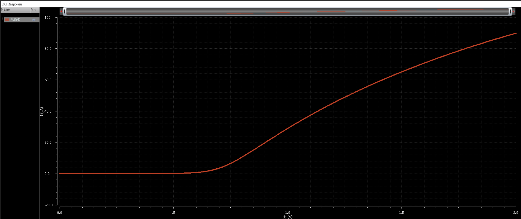
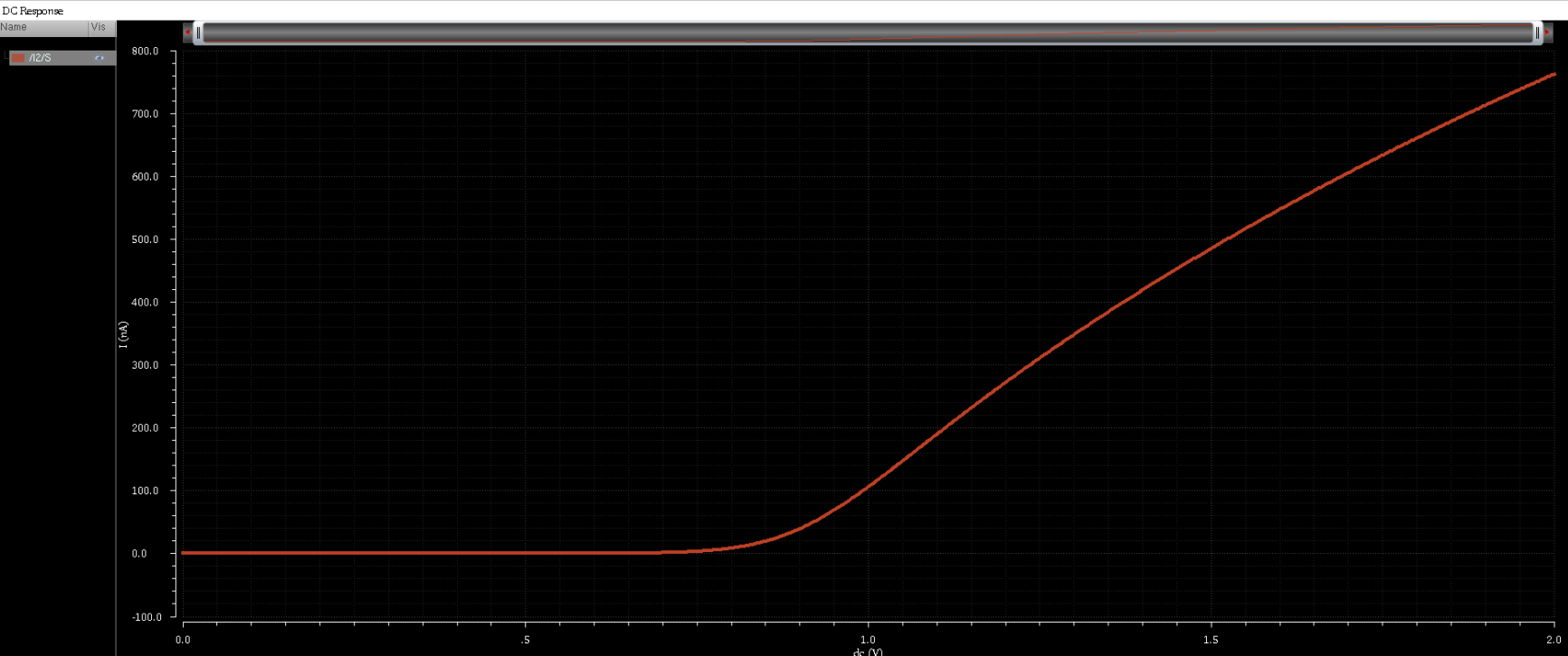
    Now we simulate the currents while sweeping Vgs/Vsg from 0V to 5V in 1mV increments. This time, the voltages Vds/Vsd is

    held at a constant 100mV.

    For NMOS:

NMOS_Ids_versus_Vgs

    For PMOS:


PMOS_Isd_versus_Vsg


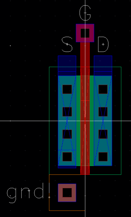
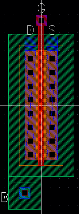
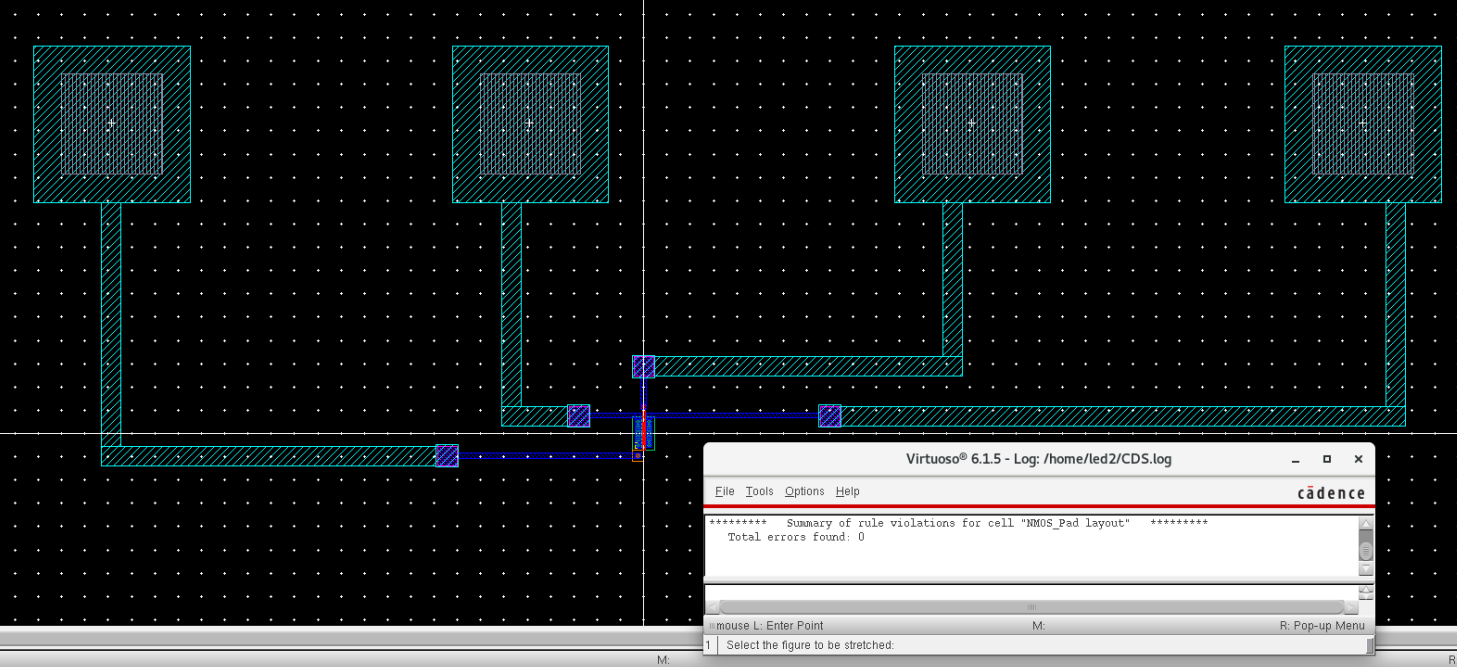
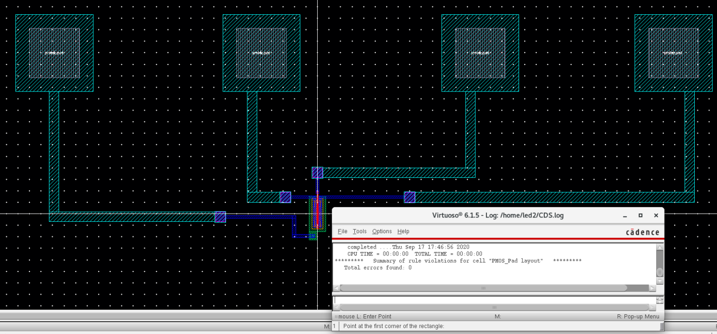
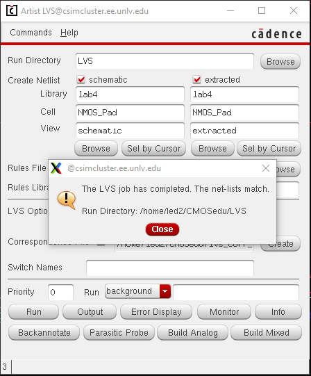
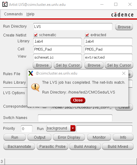
Layout of MOSFET for testing:

    Now we create a layout for the NMOS and PMOS. Our goal is to connect these layouts to test pads in order to test the

    transistors.

 
    We can use the NCSU_TechLib_ami06 library to quickly generate transistors of our desired dimension. The nmos and pmos cells
    have all the layers pre-made. We connect metal1 strips for the pins and label them.
    NMOS:
NMOS_Layout
    PMOS:
PMOS_Layout
     
    We then connected the MOSFETs to pads. Four pads are used, one for the gate, drain, source, and base.
    I stacked a 3x3 m3_m2 via cell atop a 3x3 m2_m1 via cell to reach the metal3 layer, where a pad cell allows
    probes to reach the MOSFETs. A DRC verifies that the MOSFET and pads meet the design rules.
    NMOS:
NMOS_Pad_Layout
    PMOS:
PMOS_Pad_Layout 
 
    Now we create schematics for the pads so that we can perform an LVS.
NMOS_Pad_SchematicPMOS_Pad_Schematic
   
NMOS_LVSPMOS_LVS


Return to led2 lab directory