Lab 8 - ECE 421L
25th of November, 2020
Lab Contributors
Granados Rhyan — granar1@unlv.nevada.edu
• Assisted while drafting lab report.
Le Do — led2@unlv.nevada.edu
• Provided schematics & layouts for:
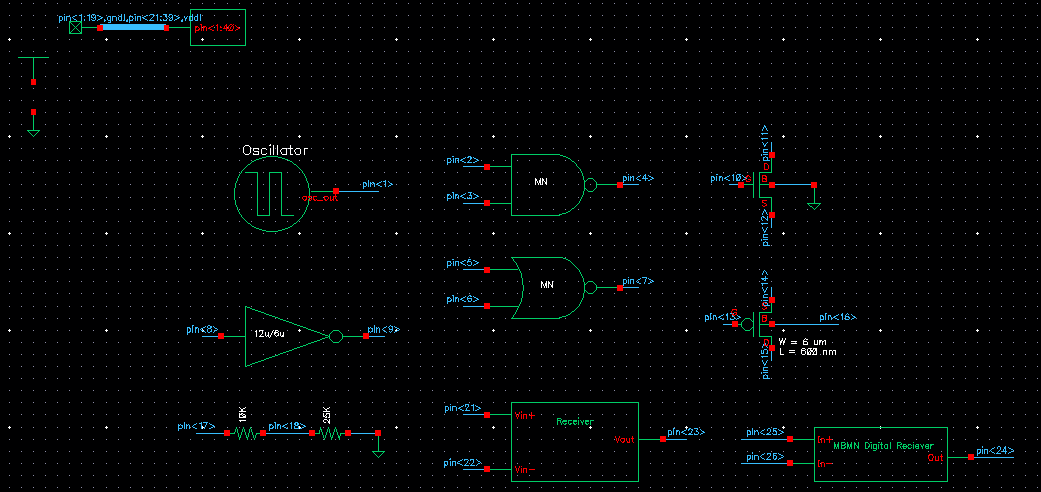
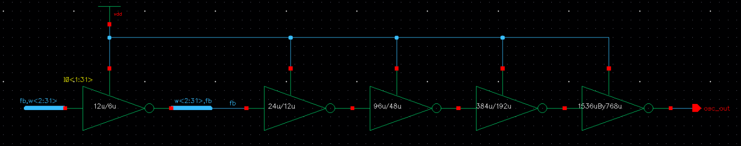
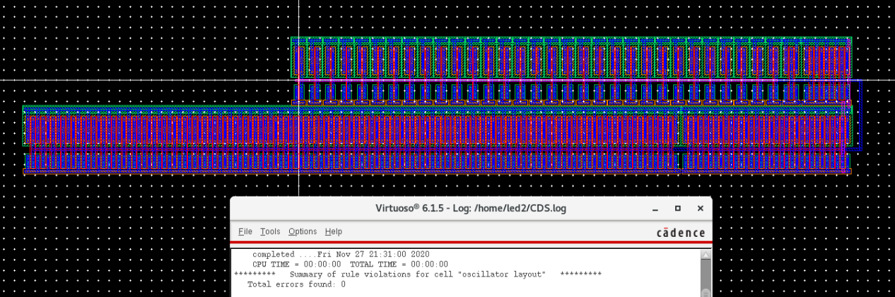
31-stage ring oscillator with buffer
12µm/6µm inverter
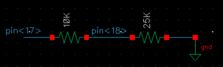
25KΩ N-Well Resistor
Voltage Divider
Lab Project
• Composed top level cell.
• Assisted while drafting lab report.
Nguyen Michael — nguyem9@unlv.nevada.edu
• Provided schematics & layouts for:
6µm/0.6µm NAND & NOR gate
6µm/0.6µm PMOS & NMOS
• Assisted while drafting lab report.
Lab Description
The following lab is about the generation of a test chip used to make real measurements
of IC circuitry. Several circuits and components are implemented in a
pad that is
prepared for fabrication. This is a team effort in which Rhyan, Do, and Michael contribute to
parts of the chip.
Prelab
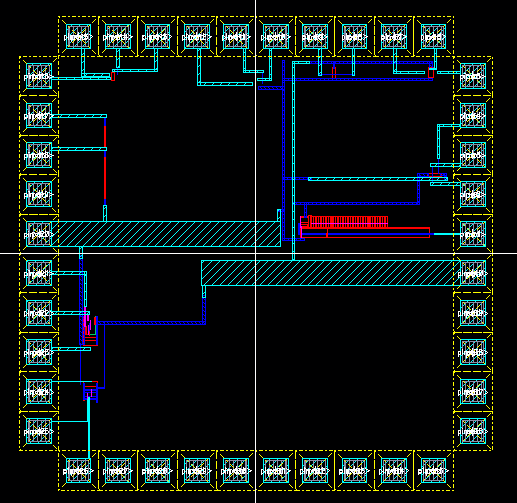
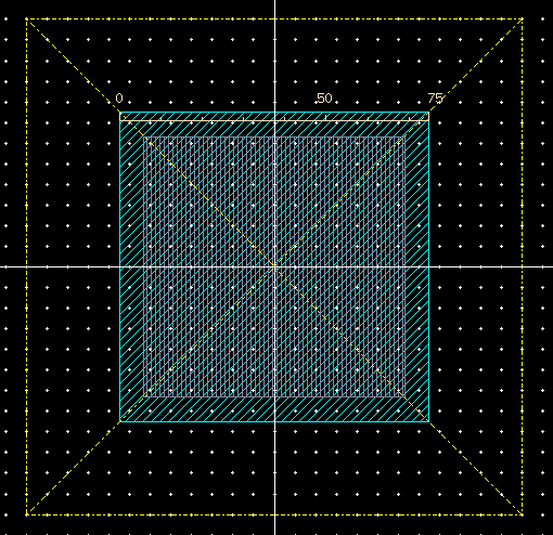
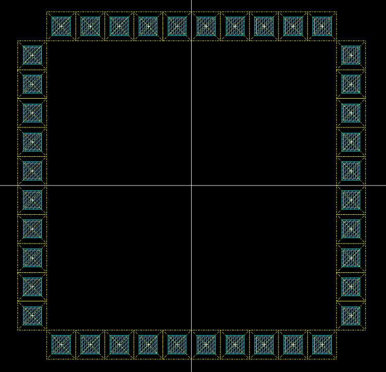
The prelab involves the creation of a 40 pin padframe. The pad frame is made up of 40
75µm x 75µm pads.
The pad consistes of a layer of metal3 with an overglass layer marked above to indicate where the
overglass will be removed during fabrication.
The pad is then formatted to be fabricated on a 75µm x 75µm chip.
The chip has 40 pins including source and ground and takes a square topology
with 10 pins per side. The following is the schematic for the pad.
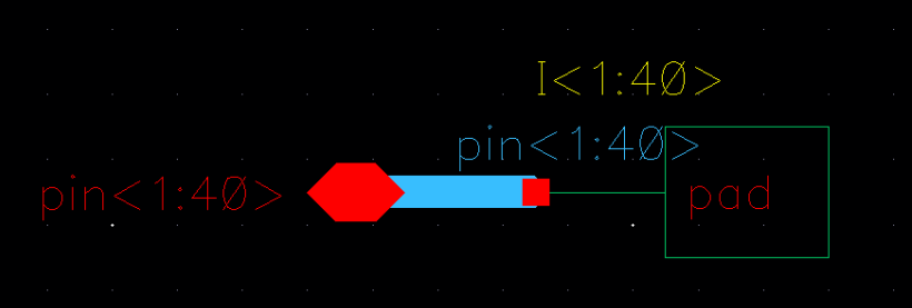
Next is the layout for the bondingpad.
With the bondingpad prepared, an IC circuit is ready to be implemented.
Lab
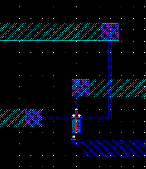
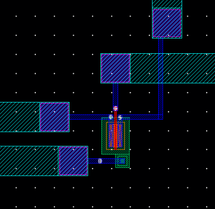
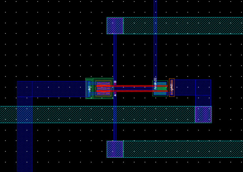
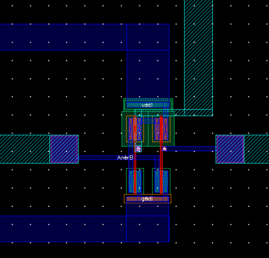
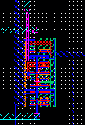
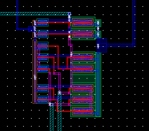
During this part of the lab, components are instantiated and added to the bonding pad.
|
Chip
Pin #
|
Pin Description
|
Comments
|
|
1
|
ocs_out | Ring oscillator output |
| Chip Pin # | Pins Description | Comments |
| 2 | A | Input A |
| 3 | B | Input B |
| 4 | A NAND B | Output A NAND B |
| Chip Pin # | Pins Description | Comments |
| 5 | A | Input A |
| 6 | B | Input B |
| 7 | A NOR B | Output A NOR B |
| Chip Pin # | Pins Description | Comments |
| 8 | A | Inverter Input |
| 9 | Ai | Inverter Output |
| Chip Pin # | Pins Description |
| 10 | NMOS Gate |
| 11 | NMOS Drain |
| 12 | NMOS Source |
| Chip Pin # | Pins Description |
| 13 | PMOS Gate |
| 14 | PMOS Source |
| 15 | PMOS Drain |
| 16 | PMOS Body |
| Chip Pin # | Pins Description |
| 17 | Voltage Divider Source |
| 18 | Voltage Divider Output |
| Chip Pin # | Pins Description | Comments |
| 19 | NoConn | No Connection |
|
20 |
Gnd | Ground pin |
|
40 |
VDD |
VDD pin |
| Chip Pin # | Pins Description | Comments |
| 21 | Project V+ | Project Postitve Input |
| 22 | Project V- | Project Negatitve Input |
| 23 | Project Vout | Project Output |
|
Chip Pin # |
Pin Description |
Comments |
|
25 |
In+ |
Positive Input |
|
26 |
In- |
Negative Input |
|
24 |
Out |
Output |