Lab 5 - EE421L
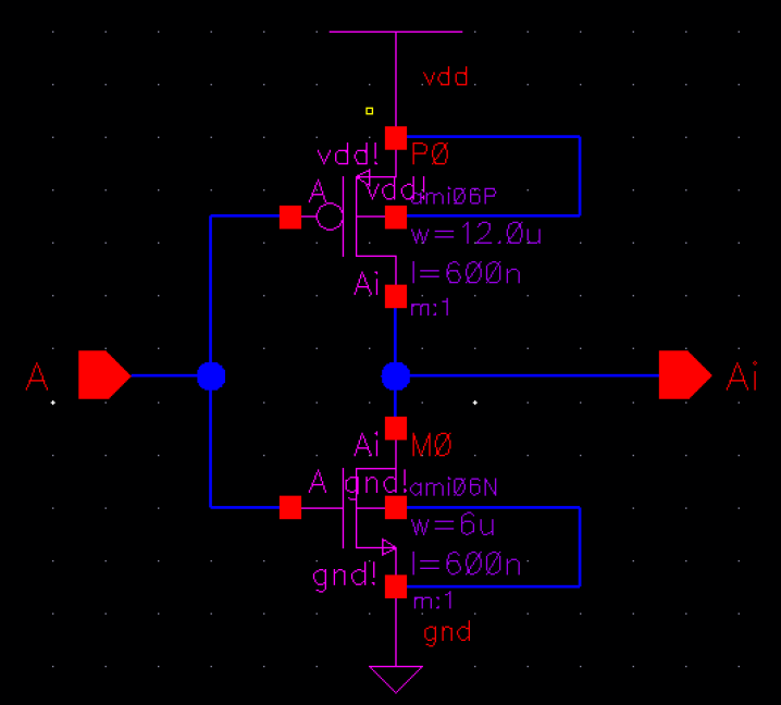
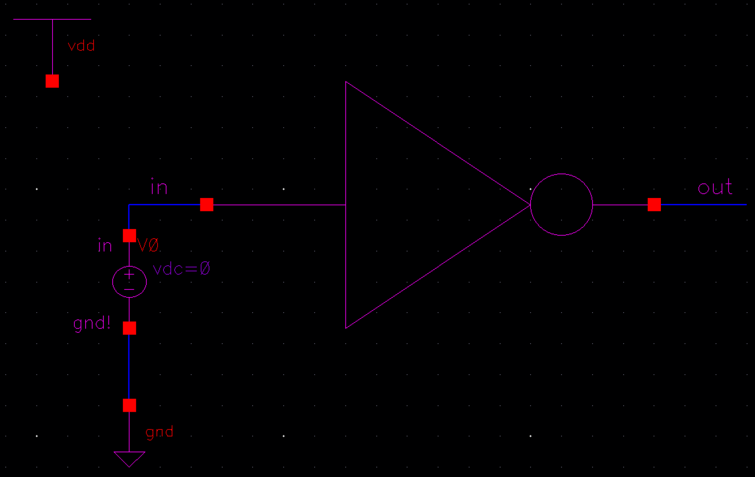
| inverter schematic |
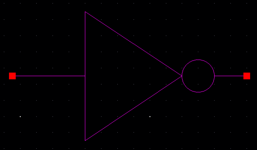
inverter symbol |
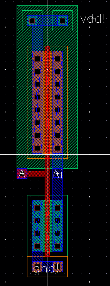
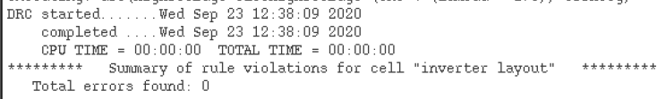
| inverter layout |
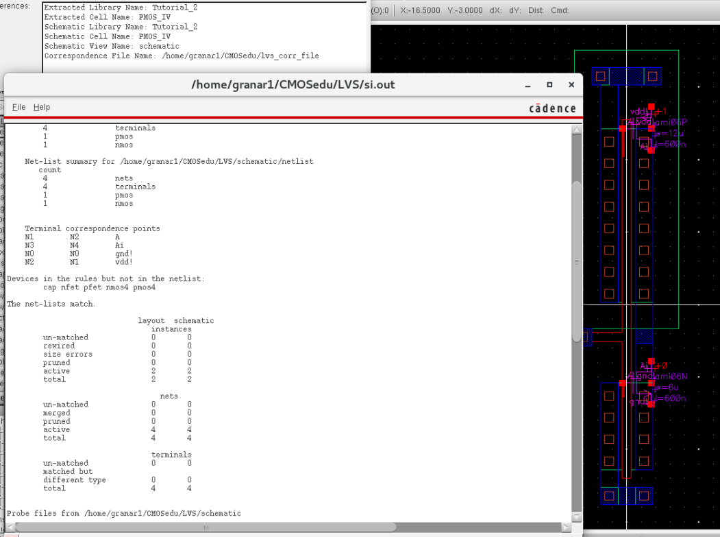
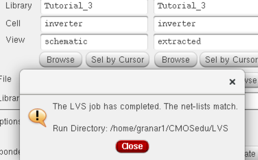
LVS Certification |
 |
 |
The Lab
1) Draft 12u/6u CMOS inverter layout and schematic
| schematic |
layout |
extracted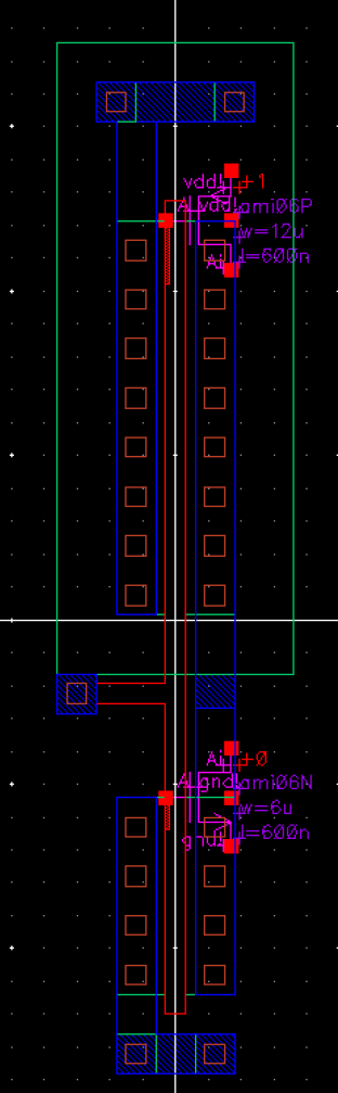 |
symbol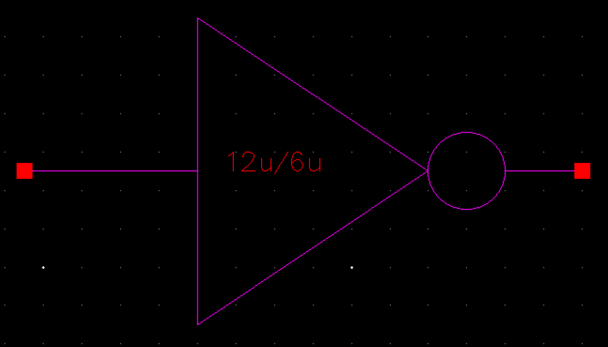 |
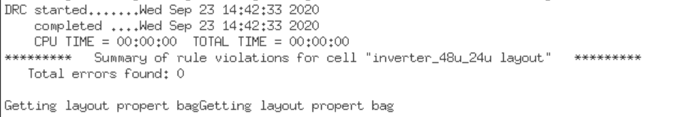
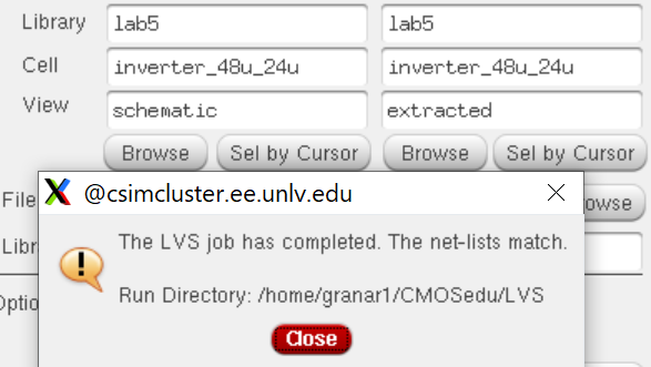
DRC and LVS certification:
 |
 |
2) Draft 48u/24u CMOS inverter layout and schematic
schematic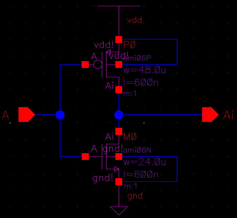 |
layout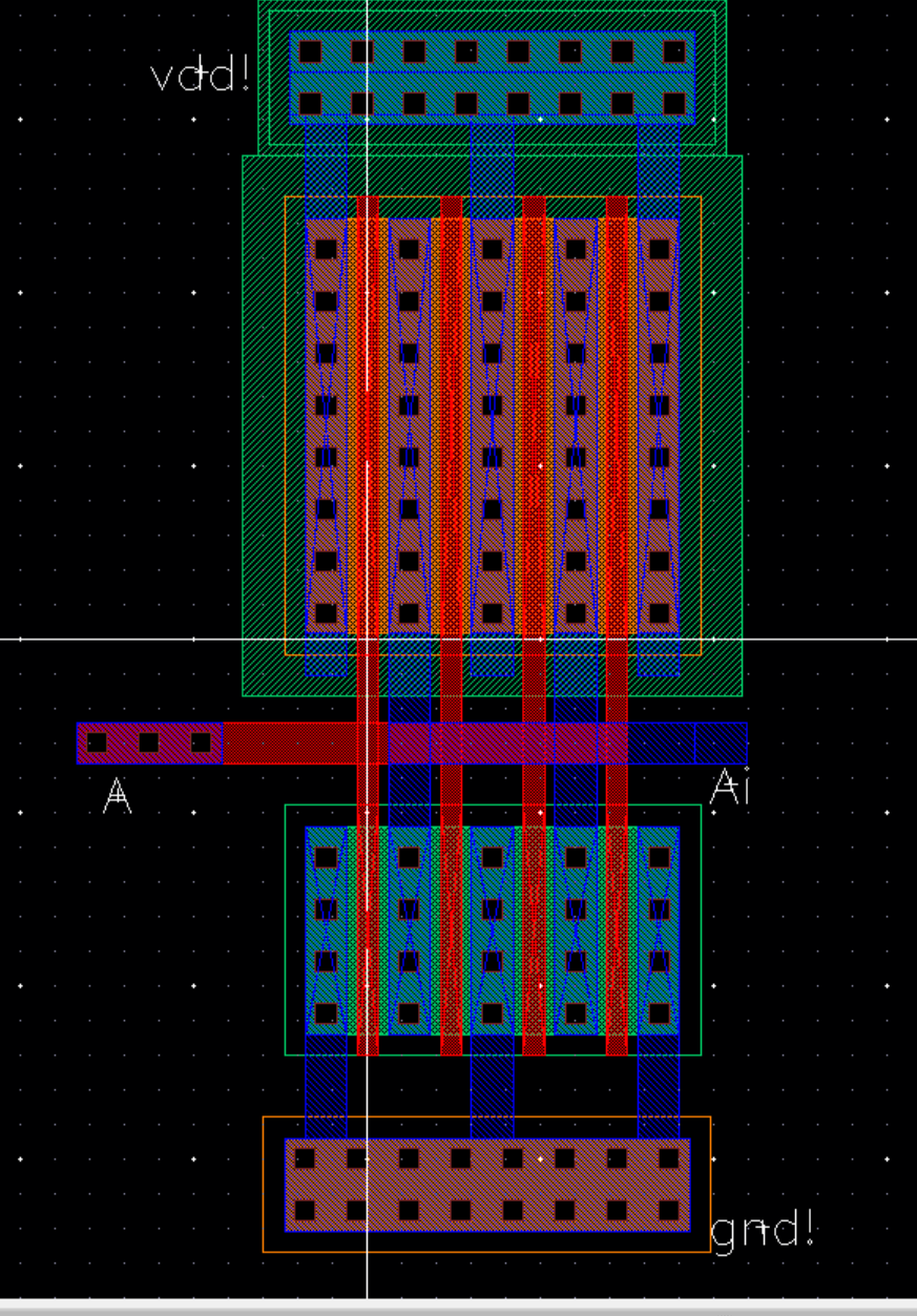 |
extracted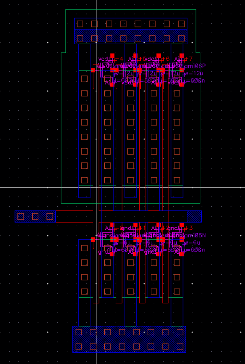 |
symbol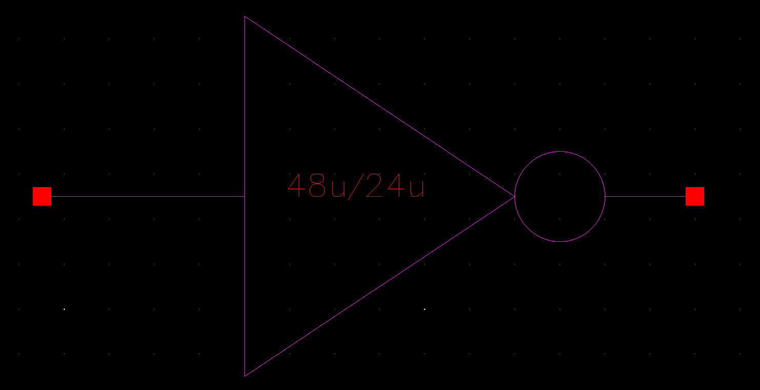 |
 |
 |
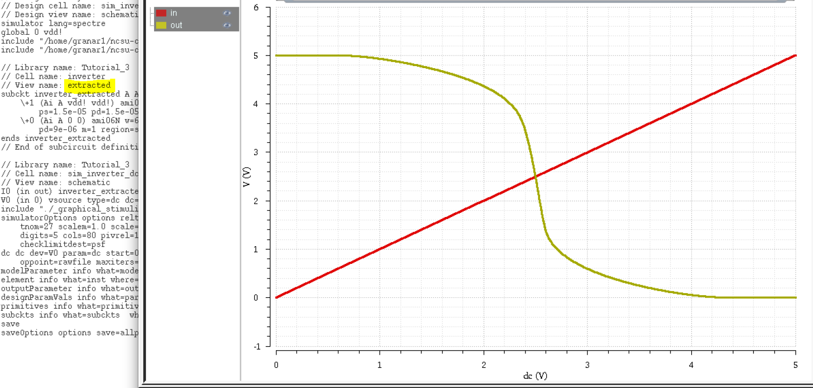
Schematic to be used for simulations:
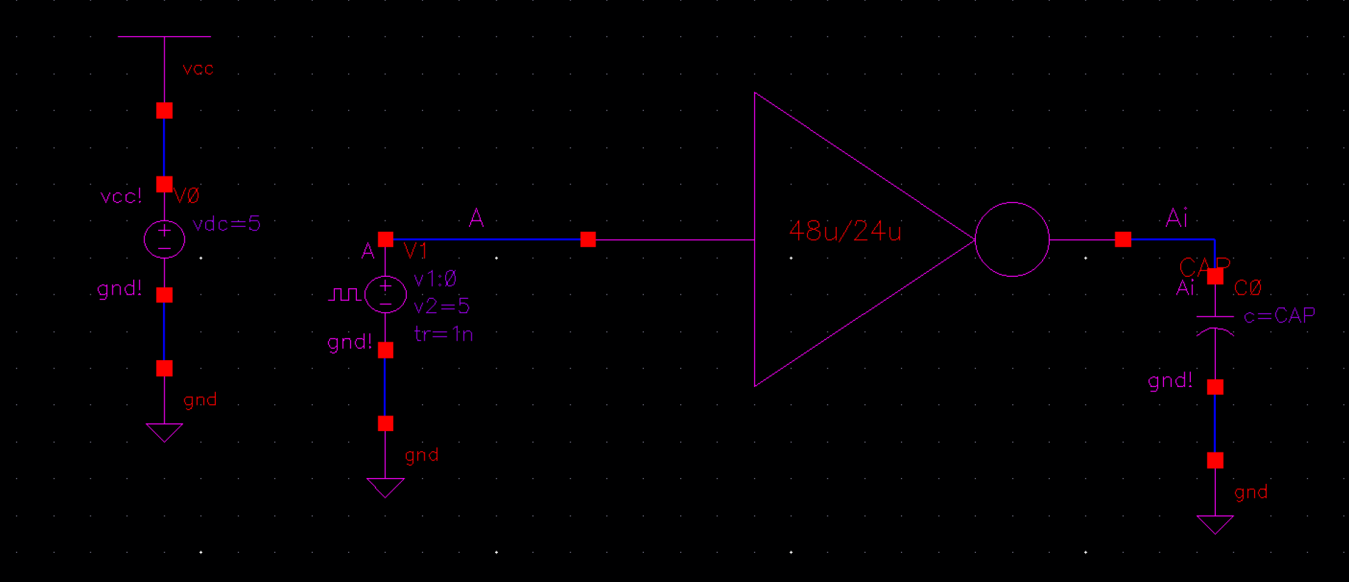
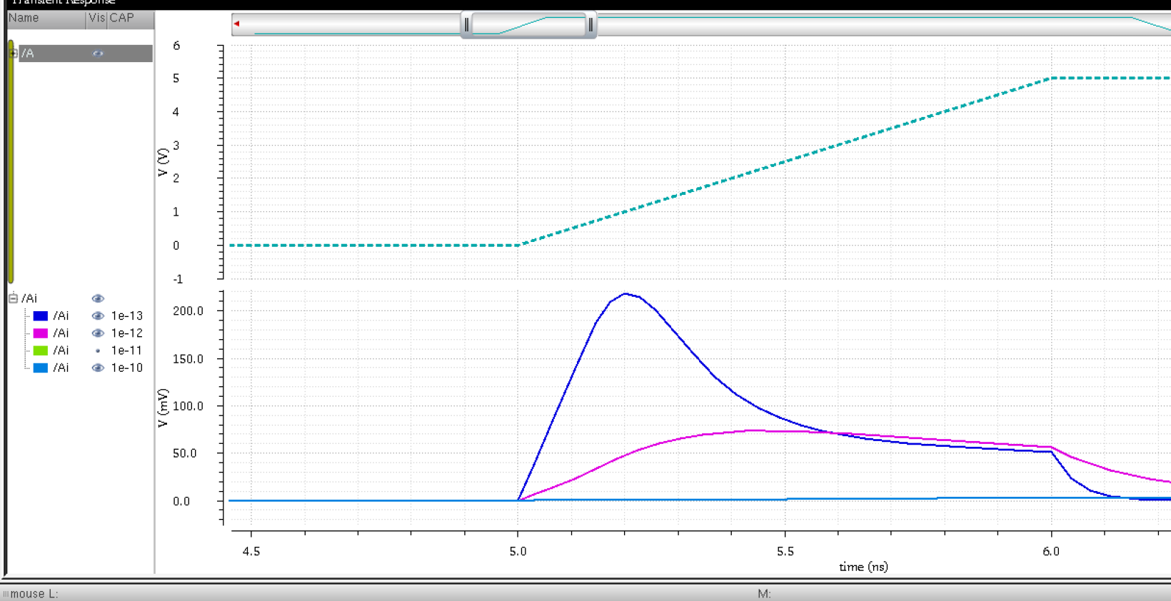
3) Driving a 100 fF, 1 pF, 10 pF, and 100 pF capacitive load with our inverter using Spectre to simulate
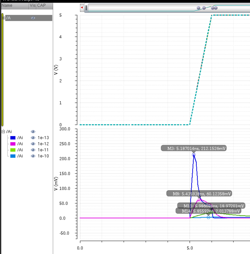 |
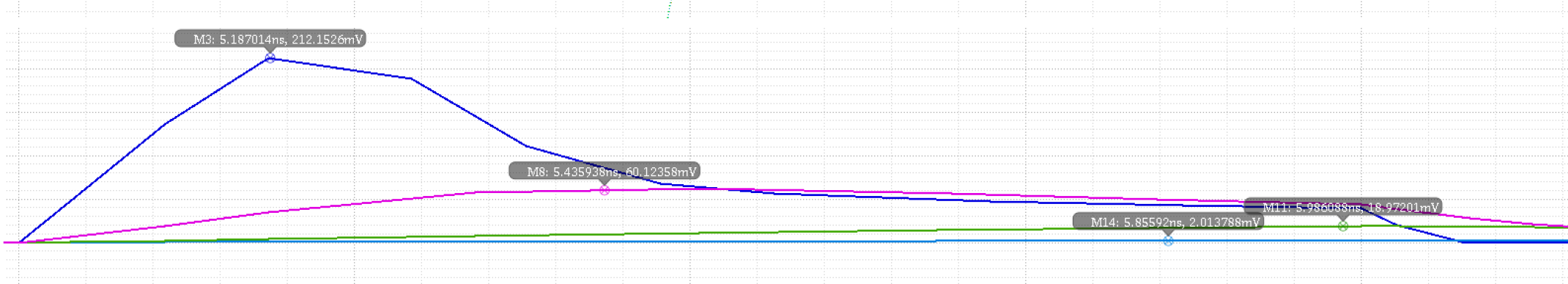 |
File Zip
File Back-up Proof