Lab
X - ECE 421L
Authored
by Ryan Castellano,
October 21, 2020
Lab
description
In this lab, I'll be designing and simulating some basic logic circuits.
Prelab:
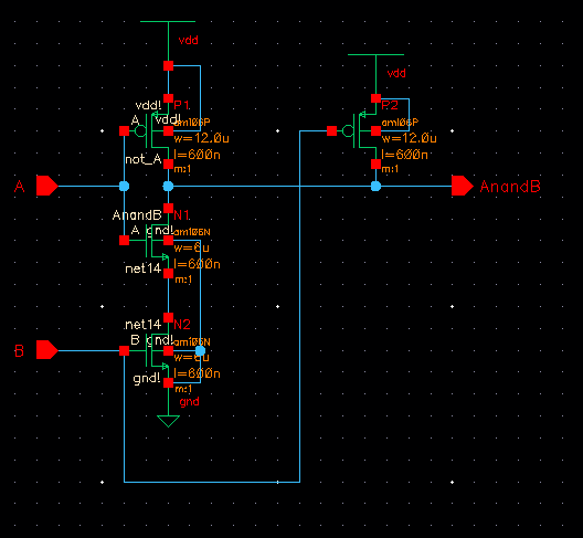
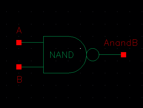
In the prelab, I worked on tutorial 4. I first created the schematic of the NAND gate and created its symbol as shown:
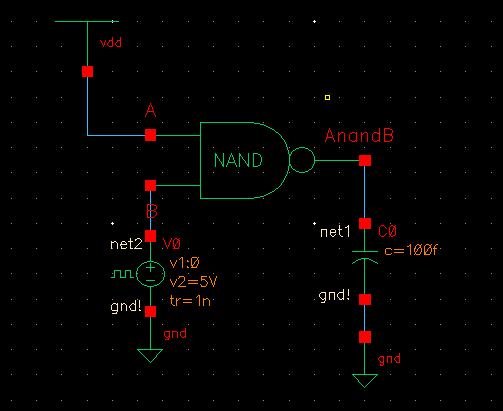
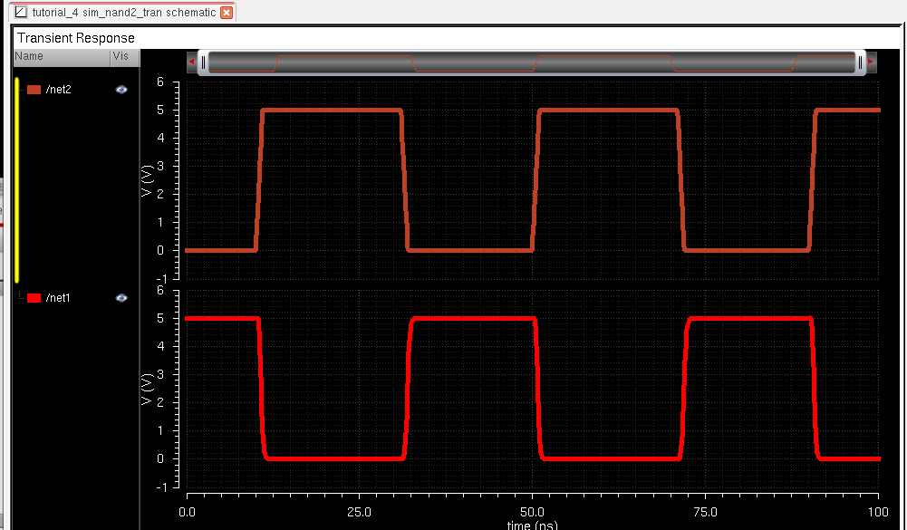
Next, I created the simulator schematic and ran it for the following results:
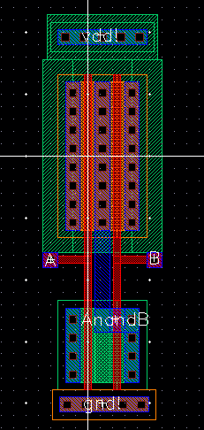
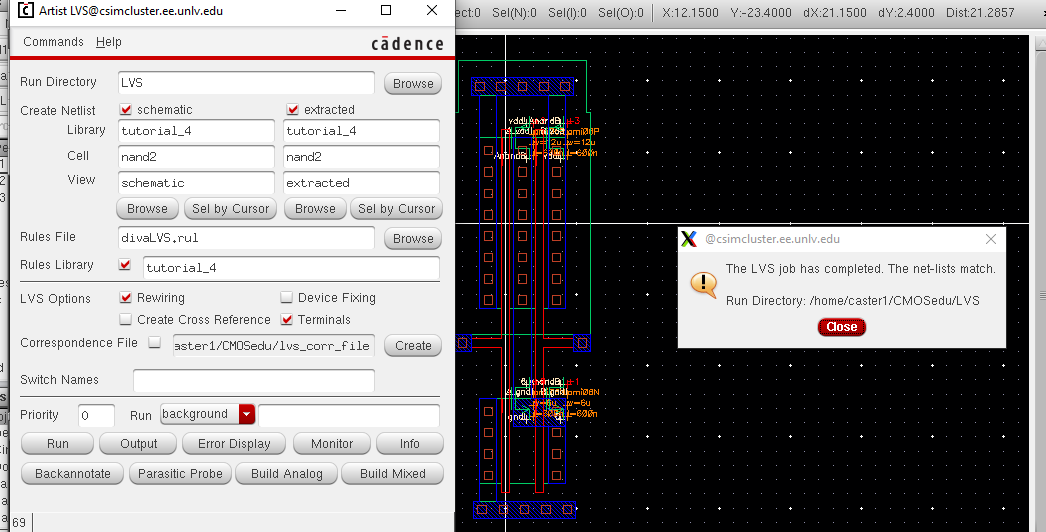
I did the layout next and extracted so I could get the LVS:
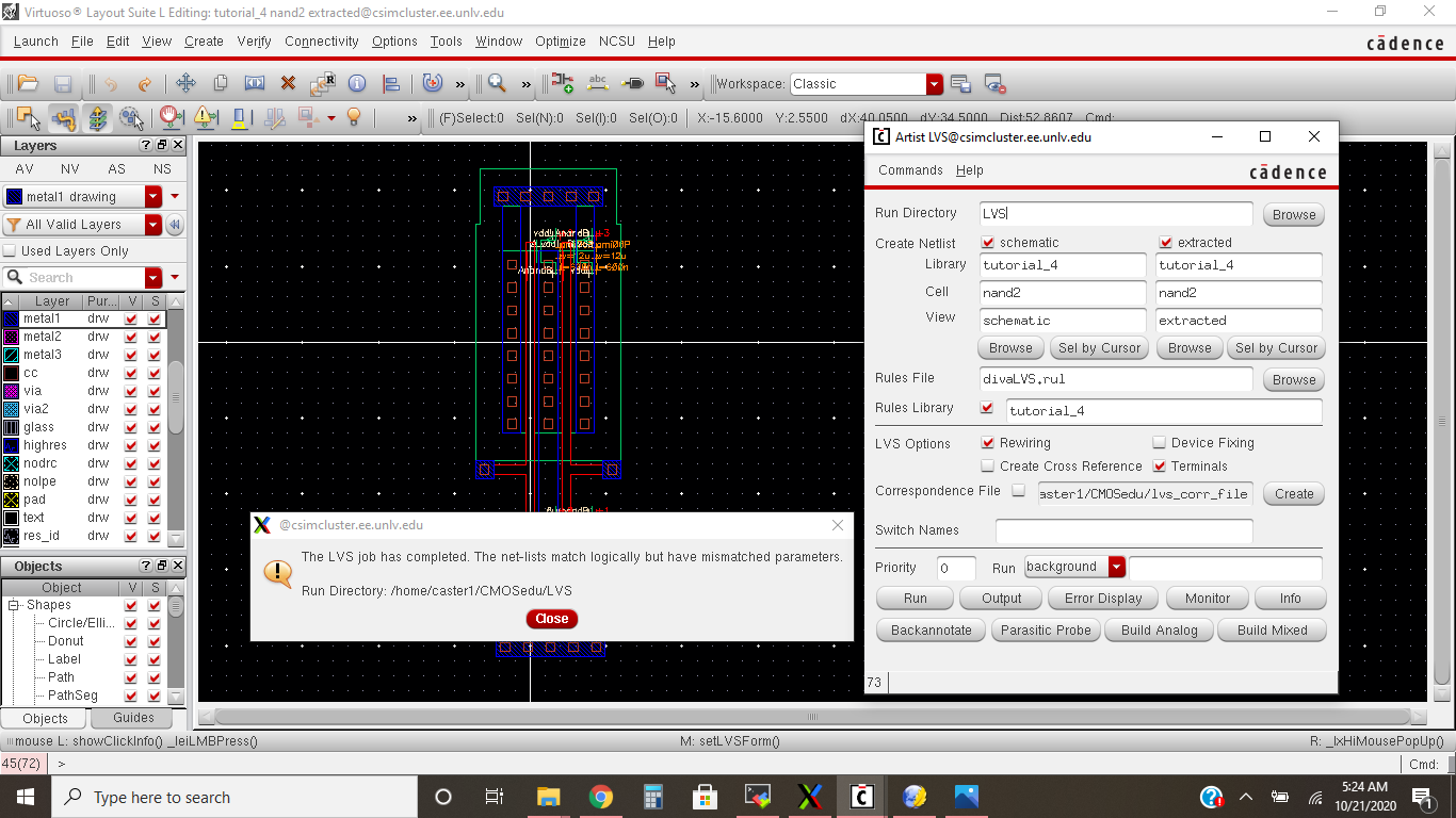
Finally, I changed the LVS rules to get the following error message:
Lab Main Content:
Since the NAND gate was done in the prelab portion, this section will focus strictly on the XOR and the full adder.
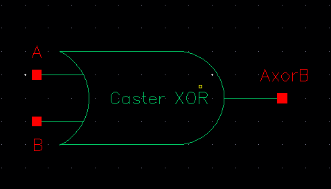
XOR Schematic and Symbol:
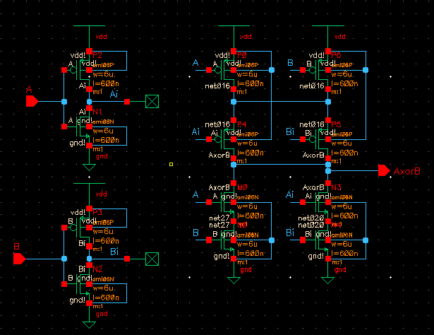
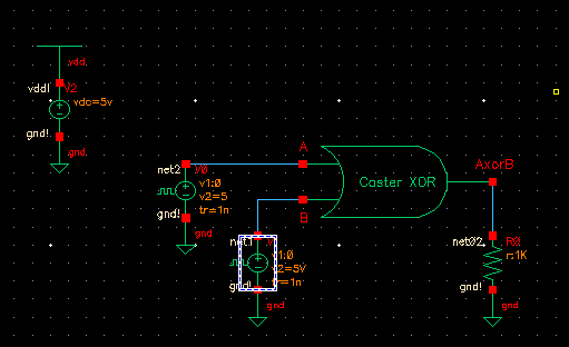
XOR simulator circuit with results:
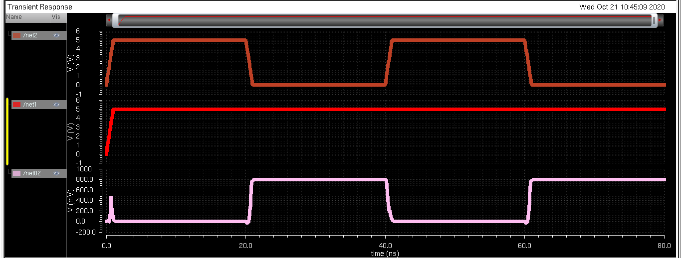
As you can see, the output is high when the inputs are opposites, proving the XOR works.
Layout, DRC, and LVS:
Return to EE 421 Labs