Lab 7 - EE
421L
Email: boloor@unlv.nevada.edu
- Back-up all of your work from the lab and the course.
- Go through Tutorial 5 seen here.
- Read through the entire lab before
starting it.
Tutorial 5
goes through the design and layout of a ring oscillator. This is demonstrated
below.
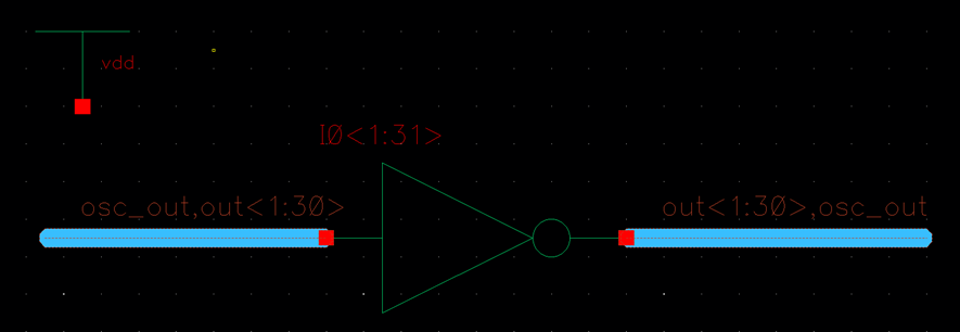
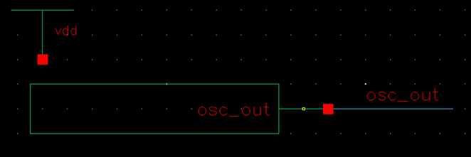
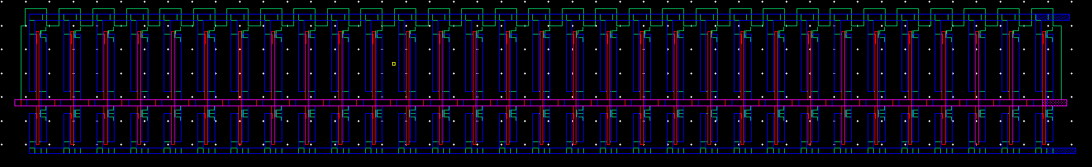
Ring Oscillator:
Schematic:
Note that the
following schematic uses a string of 31 inverters.
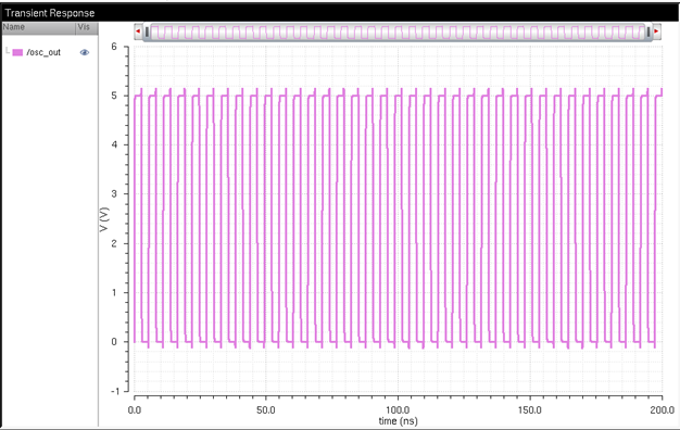
Simulation:
|
|
|
Layout with
Extracted View:
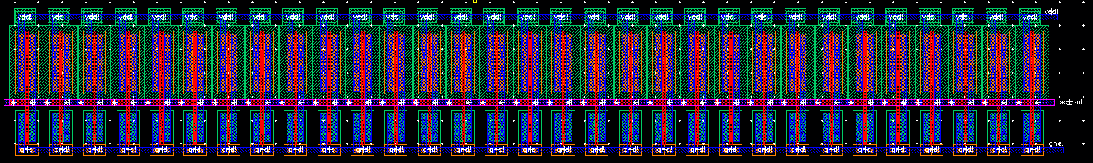
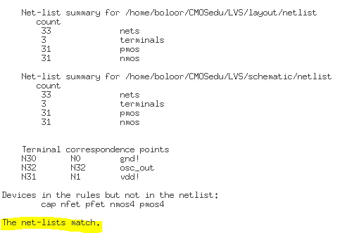
LVS and DRC
Verifications:
![]()
This concludes
the work for Tutorial 5.
The last step
I took in completing the prelab was backing up my work to my Google Drive.
Then, I read through the entirety of lab 7. This concludes the prelab.
Lab Work
·
Create a schematic, symbol and simulations for
a 4-bit word
· Show, in your lab report, how a capacitive load influences the delay and rise/fall times.
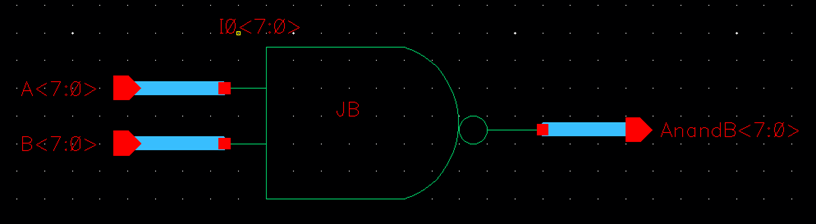
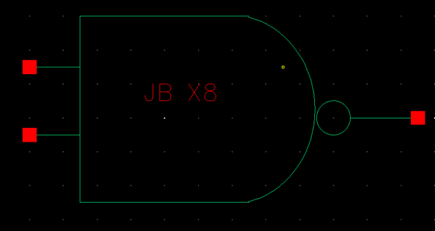
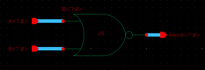
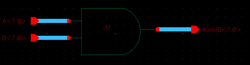
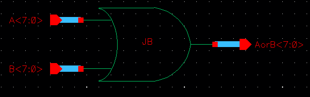
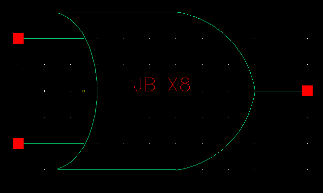
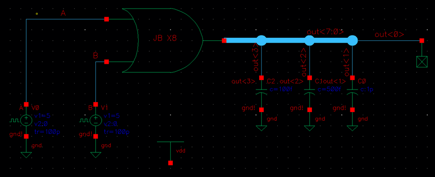
·
Create schematics and symbols for an 8-bit
input/output array of: NAND, NOR, AND, inverter, and OR gates.
o Provide a
few simulation examples using these gates.
·
Next examine the schematics given of a 2-to-1
DEMUX/MUX (and the symbol).
o Simulate the
operation of this circuit using Spectre and explain how it works.
o
Make sure to show, using simulations, how the
circuit can be used for both multiplexing and de-multiplexing.
· Create an 8-bit wide word 2-to-1 DEMUX/MUX schematic and symbol.
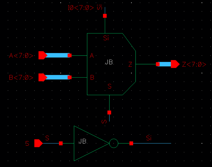
o Include an inverter in your design so the cell only needs one select input, S (the complement, Si, is generated using an inverter).
o Use simulations to verify the operation of your design.
· Finally, draft the schematic of the full-adder seen in Fig. 12.20 using 6u/0.6u devices (both PMOS and NMOS).
· Create an adder symbol for this circuit (see the symbol used in lab6).
· Use this symbol to draft an 8-bit adder schematic and symbol.
o For how to label the bus so the carry out of one full-adder goes to the carry in of another full-adder review the ring oscillator schematic discussed in Cadence Tutorial 5.
o Simulate the operation of your 8-bit adder.
· Lay out this 8-bit adder cell (*note* that this is the only layout required in this lab).
o Show that your layout DRCs and LVSs correctly.
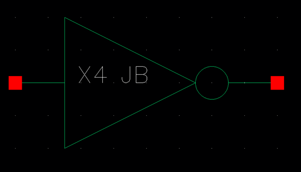
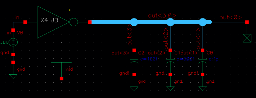
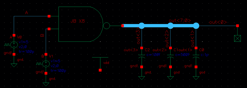
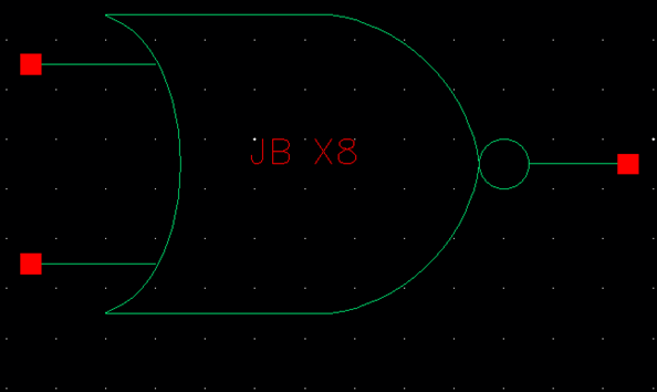
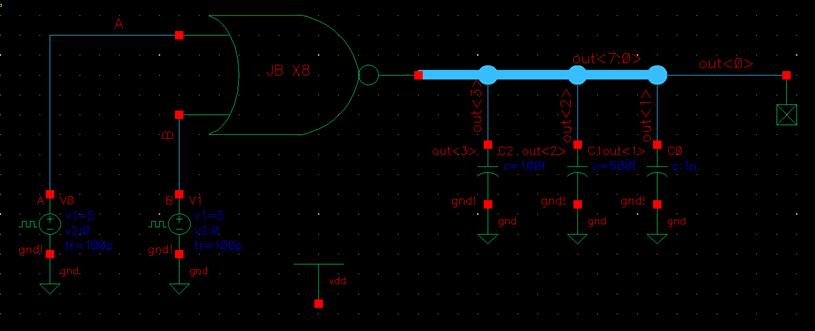
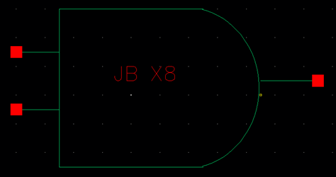
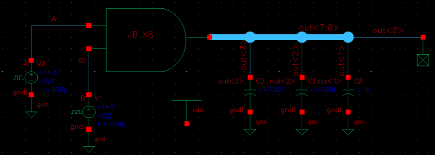
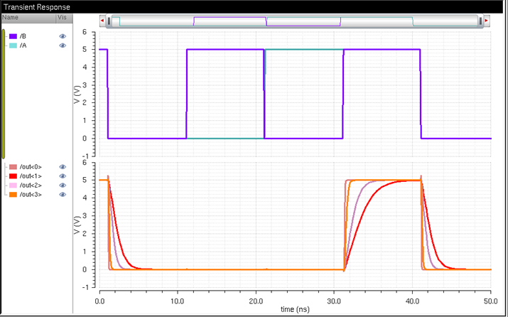
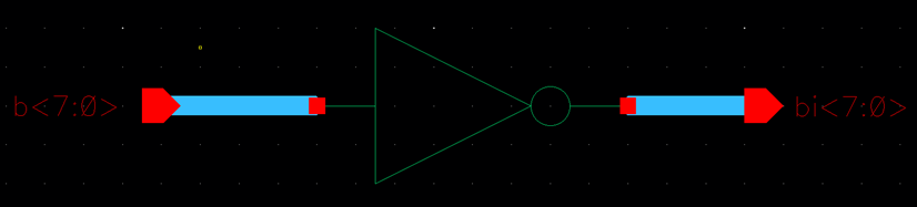
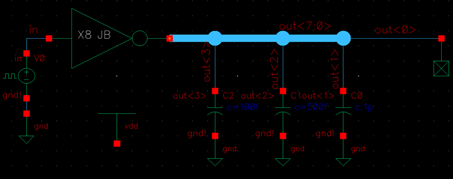
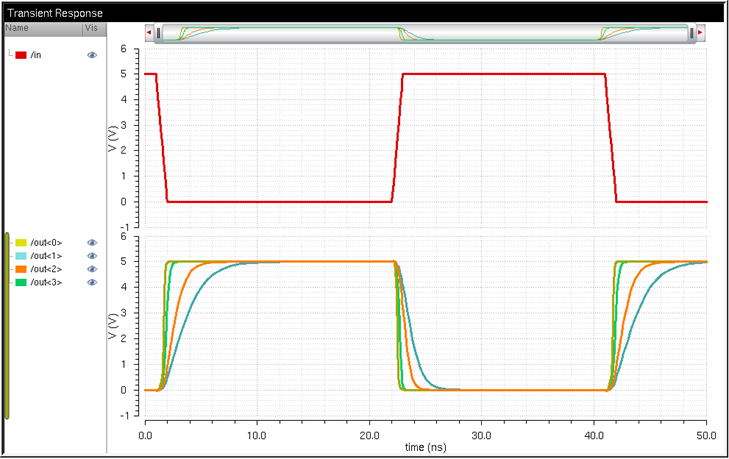
4-Bit Inverter
Schematic:
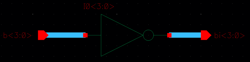
Symbol:
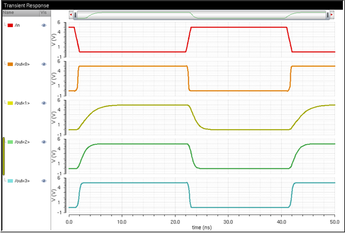
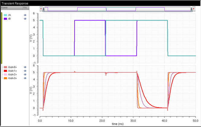
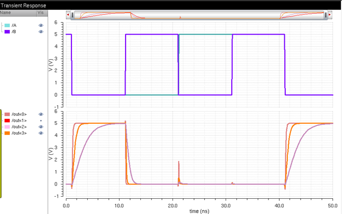
Simulation:
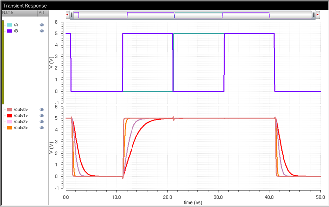
The simulation
clearly shows that as the capacitive load is increased, the rise and fall times
of the output are also increased. To be more
specific, out<3> has a 100fF capacitive load, and its rise and fall times
can compare to out<0>, which has no load. On the other hand, out<2>
and out<1> have a larger capacitance (500fF and 1pF, respectfully), and
the simulation shows that their rise and fall times are noticeably larger.
All of the following gates were simulated using different capacitive
loads to show how larger loads will increase rise and fall times, as was stated
above.
8-bit Input/Output
Array of NAND Gate:
Schematic:
Symbol:
Simulation:
8-bit Input/Output
Array of NOR Gate:
Schematic:
Symbol:
Simulation:
8-bit Input/Output
Array of AND Gate:
Schematic:
Symbol:
Simulation:
8-bit Input/Output
Array of Inverter:
Schematic:
Symbol:

Simulation:
8-bit Input/Output
Array of OR Gate:
Schematic:
Symbol:
Simulation:
2:1 MUX/DEMUX
The operation of the 2:1
MUX and DEMUX is shown below.
MUX: When the S input of the MUX is high, the output Z follows A.
When the S input of the MUX is low, the output Z follows B.
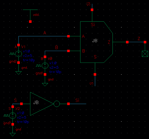
The same symbol was
used for both these simulations, meaning that the same schematic is used for
both multiplexing and demuliplexing. The above images
show that the way it is connected to inputs/outputs determine how the circuit
will act.
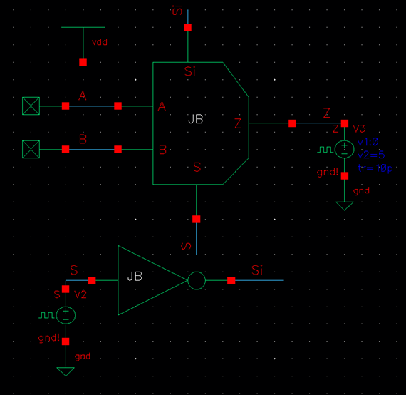
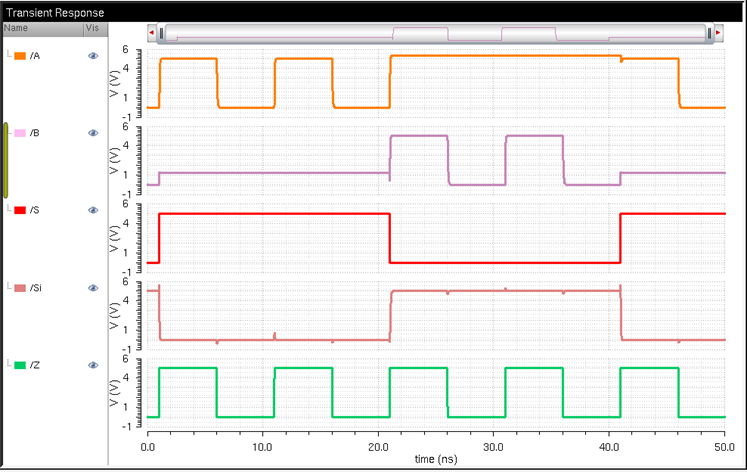
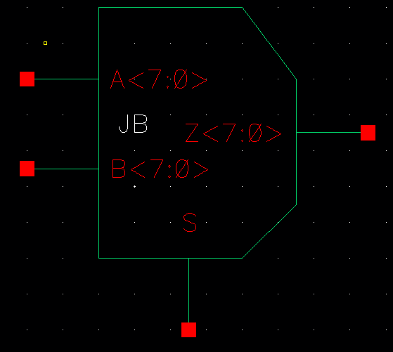
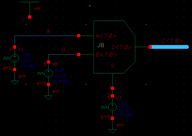
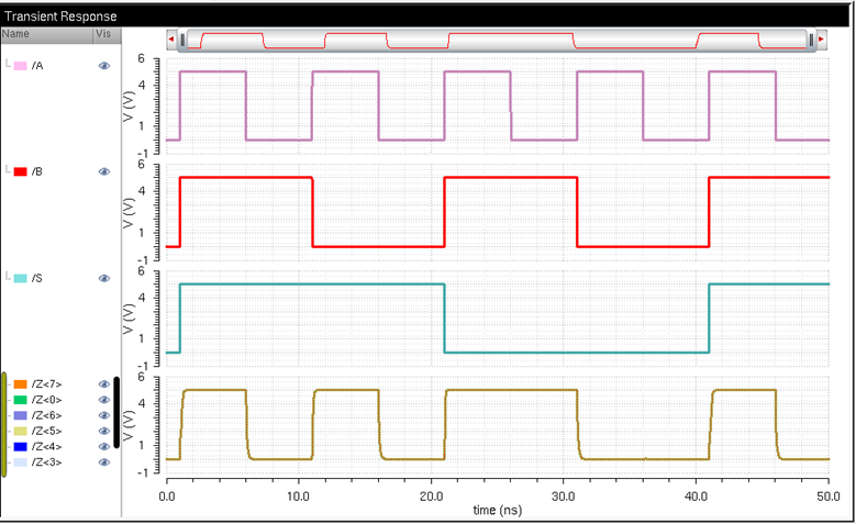
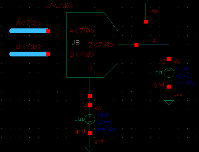
8-Bit 2:1 MUX/DEMUX
Schematic:
Symbol:
Simulation:
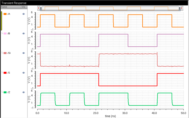
Again, we can see
that for the MUX, When the S input of the MUX is high, all 8 bits of the output
Z follow A. When the S input of the MUX is low, all 8 bits of the output Z follows
B.
MUX:
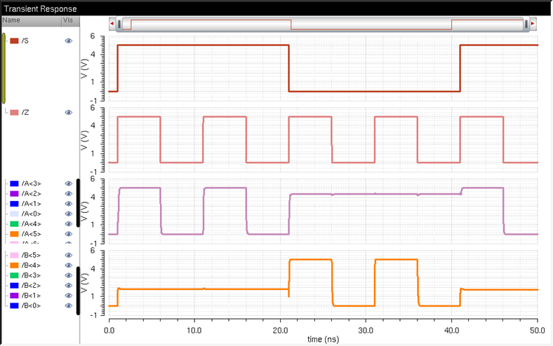
DEMUX:
Again, we can see
that when the S input of the MUX is high, all 8 bits of A is following the
output Z. When the S input of the MUX is low, all 8 bits of B is following the
output Z. When either signal is not following Z, it stays at its last known
value (either high or low).
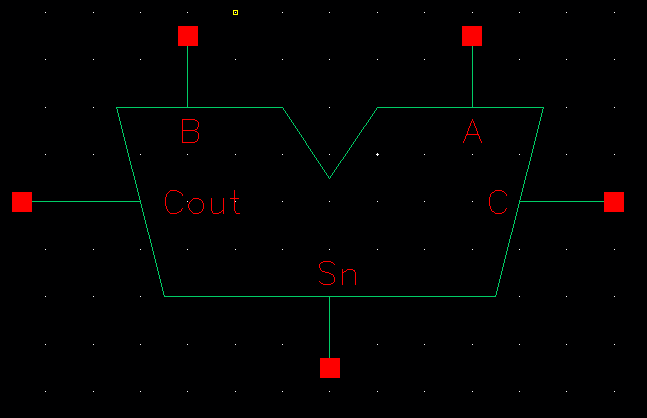
Full Adder:
Schematic:
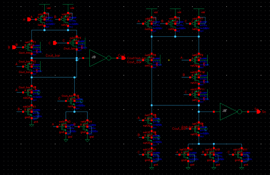
Symbol:
Layout:
Verification:
![]()
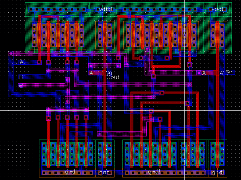
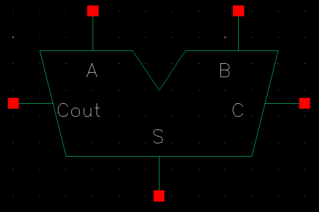
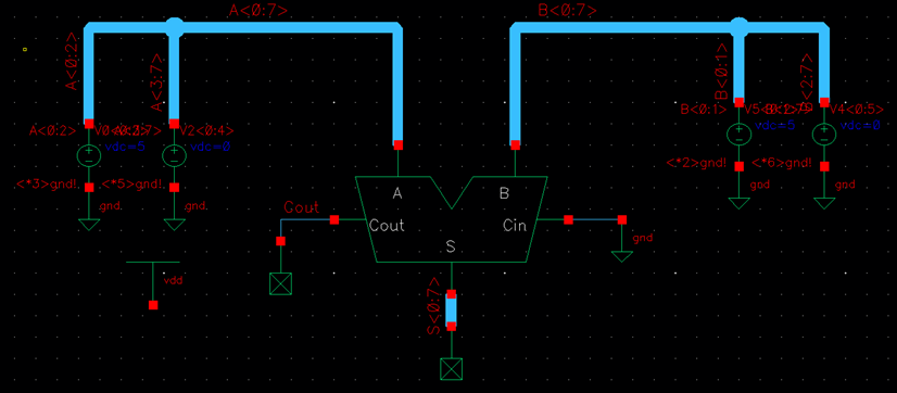
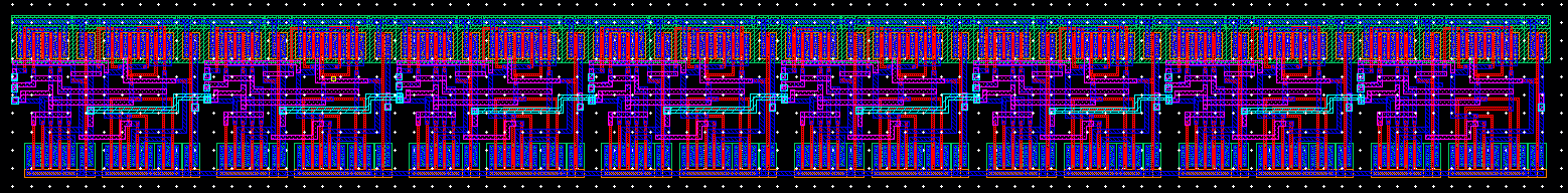
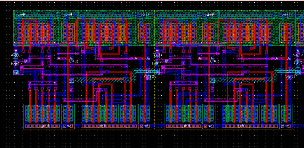
8-Bit Full Adder:
Schematic:
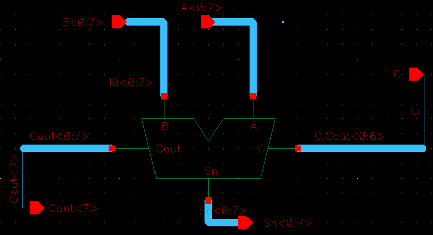
Symbol:
Simulation:
Number being
simulated: A: 00000111 = 7
B: 00000011 = 3
S: 00001010 = 10
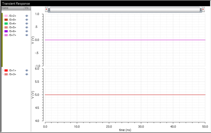
The full adder is
working as expected.
Layout with Extracted
View:
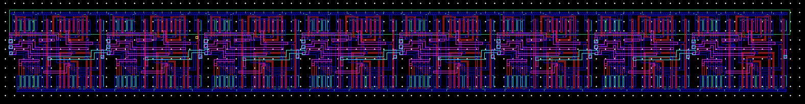
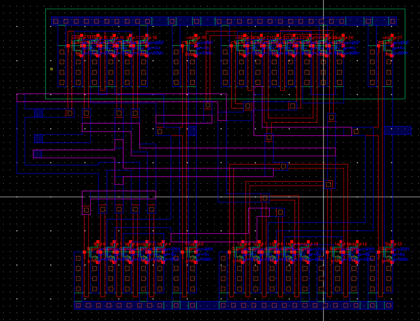
Zoomed in section of
the layout to show connections between Cout and Cin:
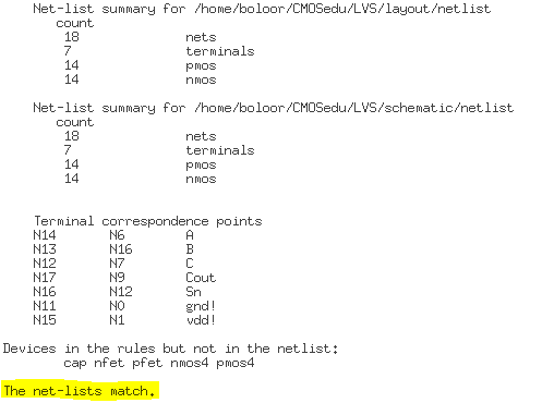
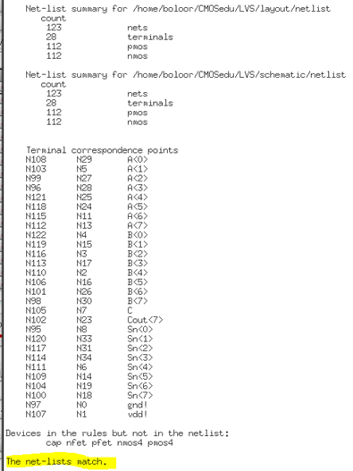
LVS and DRV Verifications:
![]()
The last step I took
in completing the lab was backing up all my work to my Google Drive.