Email: boloor@unlv.nevada.edu
- Back-up
all of your work from the lab and the course
(shown in all previous labs).
- Go
through Cadence
Tutorial 4 seen here.
Cadence Tutorial 4 goes through the design, simulation, and layout
of a CMOS NAND gate.
Design of CMOS NAND Gate
The NAND gate has the following truth table:
|
Input A |
Input B |
Output |
|
0 |
0 |
1 |
|
0 |
1 |
1 |
|
1 |
0 |
1 |
|
1 |
1 |
0 |
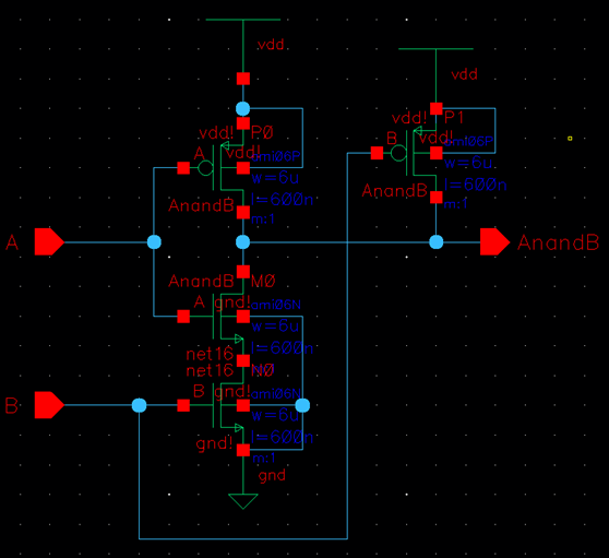
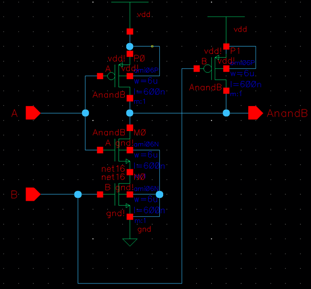
The CMOS NAND gate consists of two PMOS and two NMOS transistors,
shown below.
Simulation of CMOS NAND Gate
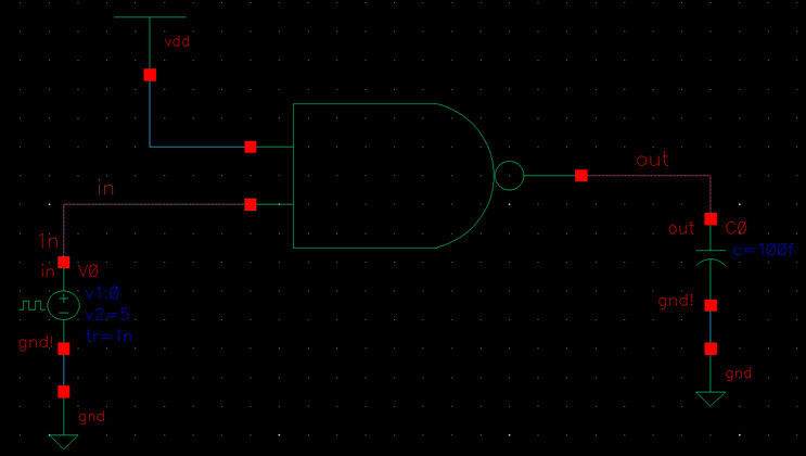
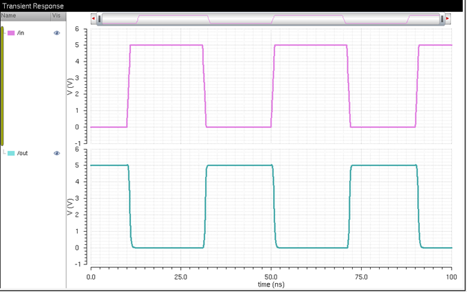
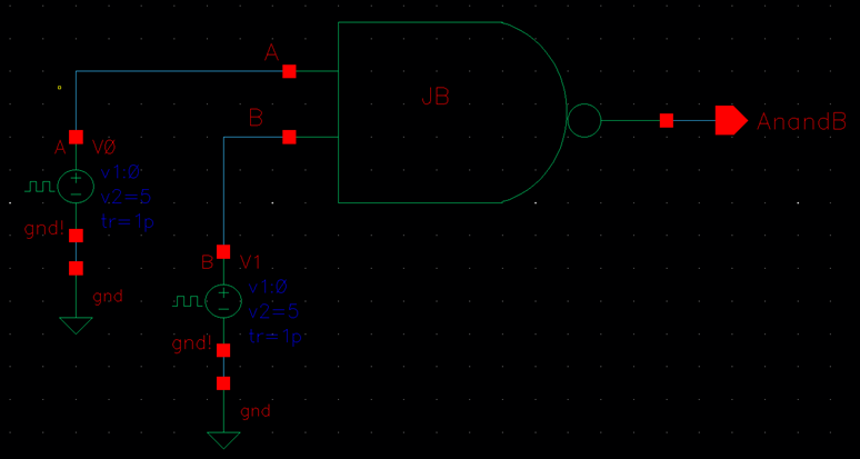
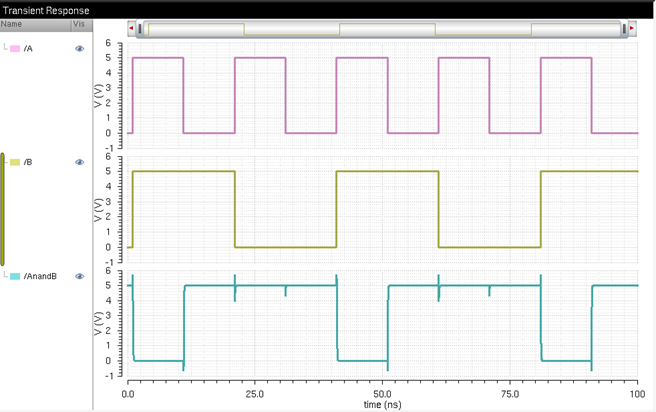
The following schematic shows the schematic drafted to test the
NAND gate, as well as its simulated results. When operating correctly, a NAND
gate should output high unless both of its inputs are high. Since the top
terminal of the NAND gate is tied high, the output changes with the pulse shown
in the bottom terminal. When this pulse is high, both terminals of the NAND are
high, so the output is low. When this pulse is low, only one terminal of the
NAND is high, so the output is low. The logic gate is working correctly.
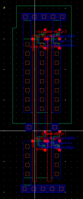
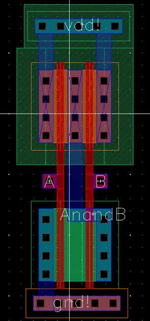
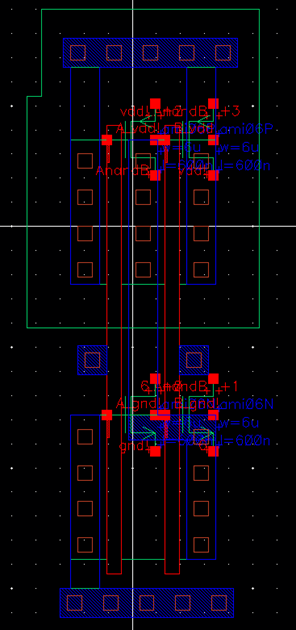
Layout of CMOS NAND Gate
The layout and extracted views of the NAND gate are shown below,
along with their DRV and LVS verification.
|
|
|
|
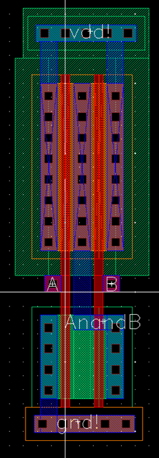
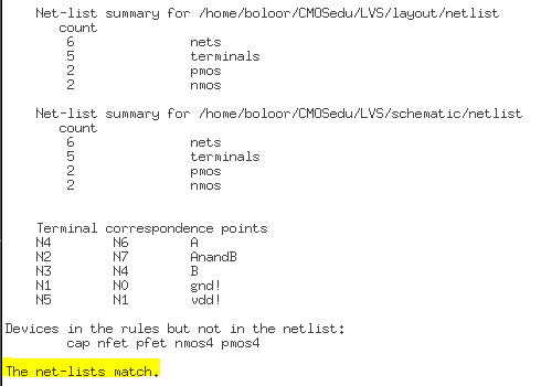
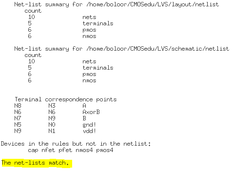
Note that the tutorial leads us through designing a NAND gate
whose PMOS devices are 12u/600n in the layout, but 6u/600n in the schematic.
Though the LVS will still show verification, comparing device sizes can be
added to the parameters that the LVS checks by going to NCSU > Modify LVS
Rules > Compare FET parameters. The following LVS message will appear after
the size parameters are added:
![]()
The last step I took
for the prelab was backing up my work. This concludes Tutorial 4, as well as
the prelab.
Lab Work:
- Draft the schematics of a
2-input NAND gate (Fig. 12.1), and a 2-input XOR gate (Fig. 12.18) using
6u/0.6u MOSFETs (both NMOS and PMOS)
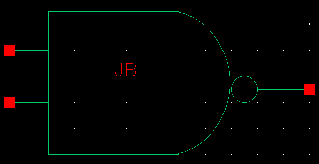
- Create layout
and symbol views for these gates showing that the cells DRC and LVS
without errors
- ensure that
your symbol views are the commonly used symbols (not boxes!) for these
gates with your initials in the middle of the symbol
- ensure all
layouts in this lab use standard cell frames that snap together
end-to-end for routing vdd! and gnd!
- use
a standard cell height taller than you need for these gates so
that it can be used for more complicated layouts in the future
- ensure gate
inputs, outputs, vdd!, and gnd! are all
routed on metal1
- Use cell names
that include your initials and the current year/semester
- Using Spectre simulate the logical operation of the gates
for all 4 possible inputs (00, 01, 10, and 11)
- comment on
how timing of the input pulses can cause glitches in the output of a
gate
- Your html lab
report should detail each of these efforts
- Using
these gates, draft the schematic of the full adder
- Create a symbol for this full-adder
- Simulate, using Spectre, the
operation of the full-adder using this
symbol
- Layout
the full-adder by placing the 5 gates end-to-end
so that vdd! and gnd!
are routed
- full-adder inputs and outputs can be on metal2 but not
metal3
Designing the 2-Input NAND Gate:
The truth table for the NAND gate was shown in the prelab.
Simulation:
The simulation below
clearly follows the truth table for the NAND gate – the output is high for all
inputs except when both inputs are high. Glitches can be seen in the output
of the simulation; they can be attributed to the fact that the input signals
are pulses. The glitches occur during the small rise/fall time of these pulse
signals, as the inputs at those picoseconds are not perfect high/low values.
Layout with
Extracted View and LVS / DRC Verifications:
|
|
|
|
Designing the 2-Input XOR Gate:
The XOR gate has the following truth table:
|
Input A |
Input B |
Output |
|
0 |
0 |
0 |
|
0 |
1 |
1 |
|
1 |
0 |
1 |
|
1 |
1 |
0 |
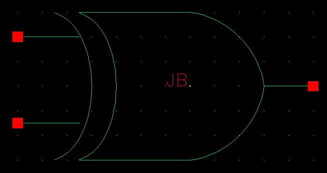
Schematic and Symbol:
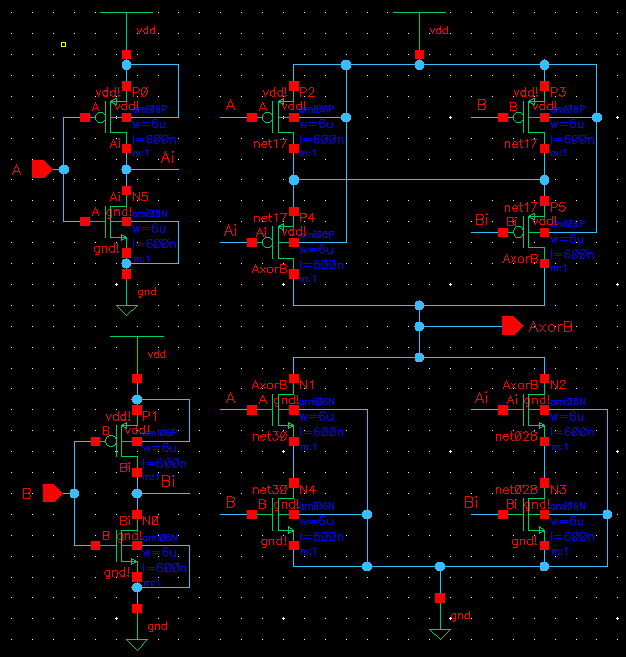
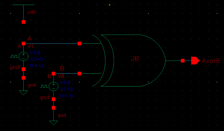
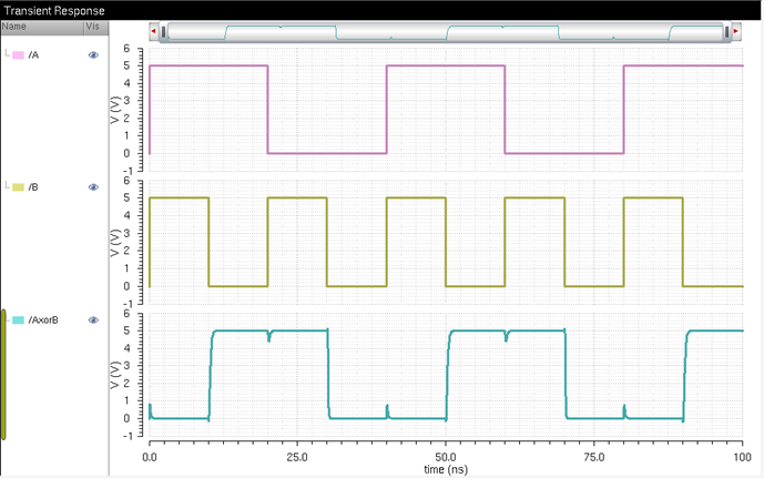
Simulation:
The simulation below clearly follows the truth table for the XOR
gate – the output is high when the inputs are not the same. Glitches can be
seen in the output of the simulation for the same reasons mentioned earlier -
the gate is not reading a clear value at those moments.
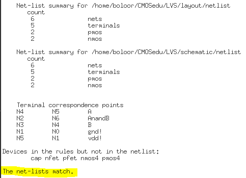
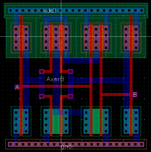
Layout with Extracted View and LVS / DRC Verifications:
|
|
|
|
|
|
|
|
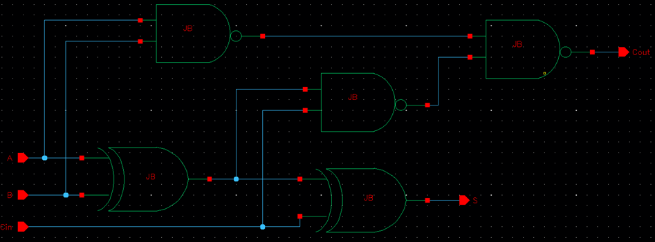
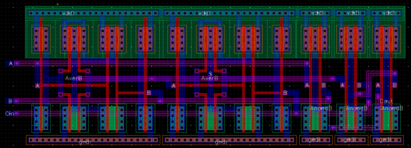
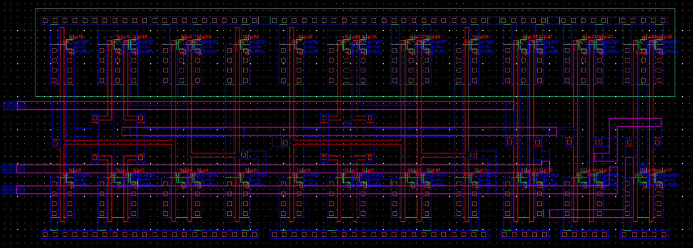
Designing the Full Adder:
The full adder
was drafted using the NAND and XOR gates shown above. It has the following
truth table:
|
A |
B |
Cin |
S |
Cout |
|
0 |
0 |
0 |
0 |
0 |
|
0 |
0 |
1 |
1 |
0 |
|
0 |
1 |
0 |
1 |
0 |
|
0 |
1 |
1 |
0 |
1 |
|
1 |
0 |
0 |
1 |
0 |
|
1 |
0 |
1 |
0 |
1 |
|
1 |
1 |
0 |
0 |
1 |
|
1 |
1 |
1 |
1 |
1 |
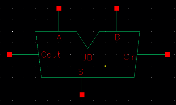
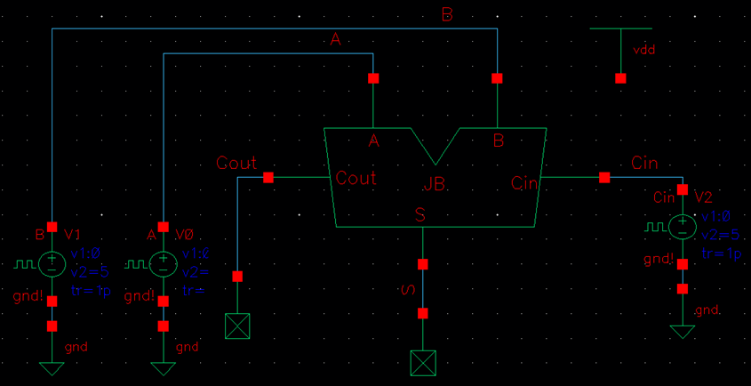
Schematic and Symbol:
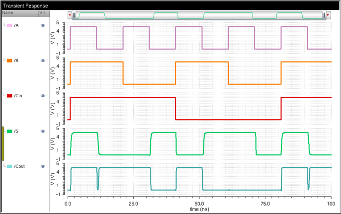
Simulation:
The simulation below resembles the information shown in the truth
table above – the sum of the three inputs is added and then represented by Sum
and Cout. Again, the glitches seen in the output
of the simulation are due to the full adder not reading clear high/low values
at the rise and fall times of the input pulses.
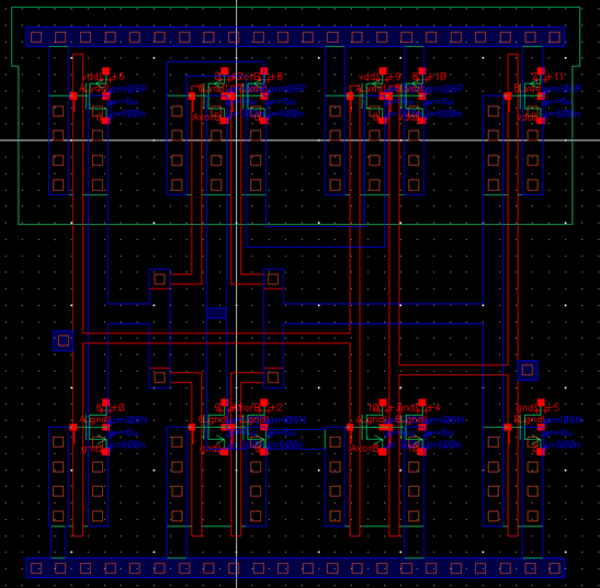
Layout with Extracted View and LVS / DRC Verifications:
![]()

Lastly, I backed up all my work
to my Google Drive.
This concludes lab 6.