Lab 5 - EE
421L
Email: boloor@unlv.nevada.edu
·
Back-up all of your work from the lab and
the course.
·
Go through Tutorial
3 seen here.
All of my lab work thus far has been
backed up, as shown in previous reports.
Tutorial 3 goes
through the design, layout, and simulation of a CMOS inverter. The following
images show each of these steps.
Design of CMOS
inverter:
![]()
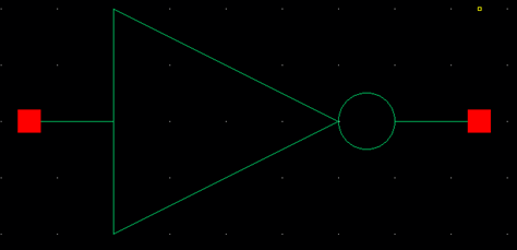
Internal schematic for the inverter Inverter symbol created
Layout of CMOS
inverter:

Inverter layout Inverter layout extracted view
Simulation of CMOS
inverter:
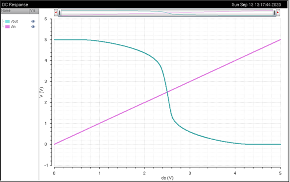
The inverter performs as expected – the output is high when the
input is low and vice versa. Note that the simulation for the extracted view
was the same as the simulation for the schematic above.
To conclude the
prelab, I backed up my work up to my Google drive again.
- Draft
schematics, layouts, and symbols for two inverters having sizes of:
- 12u/6u (= width of the PMOS / width of the NMOS with
both devices having minimum lengths of 0.6u)
- Your
schematics should have two pins, e.g., A and Ai
- Your layouts
should have 4 pins: A, Ai, vdd!, and gnd! (note
how lowercase letters are used for power and ground)
- Your lab
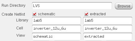
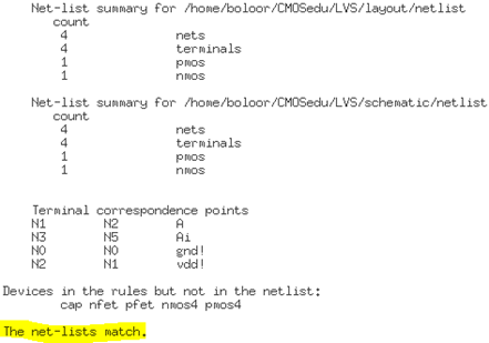
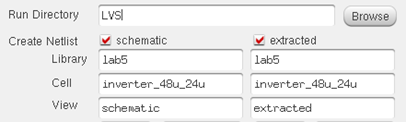
reports should document your efforts and results including showing that
the extracted layouts and schematics LVS correctly
- Zip up these
cells in a directory: lab5_jeb
- Using SPICE simulate the
operation of both of your inverters showing each driving a 100 fF, 1 pF, 10 pF, and 100 pF capacitive load
- Comment, in
your report, on the results
- Use
UltraSim (Cadence's fast SPICE simulator for
larger circuits at the cost of accuracy) and repeat the above
simulations
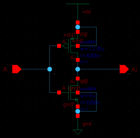
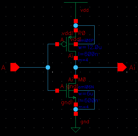
The 12u/6u Inverter:
Note that this design closely followed the one made for the
prelab. Also note that the design has two pins on the schematic (A and Ai), and
four pins on the layout (vdd!, gnd!, A, Ai).
Design of 12u/6u
inverter:
![]()

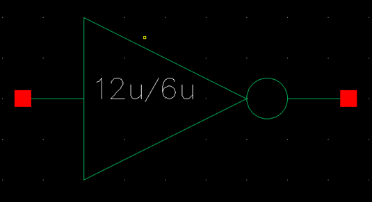
Internal schematic for the inverter Inverter symbol created
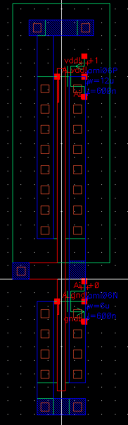
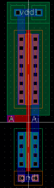
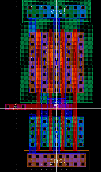
Layout of 12u/6u inverter
(with verification):
|
Inverter
layout |
Inverter layout extracted view |
DRC and LVS verification |

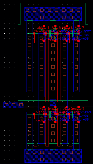
The 48u/24u Inverter:
Note that this design
uses a device multiplier (m) of 4, meaning 4 MOSFETS are used in parallel when
specified. Also note that the layout still has the same four pins mentioned
above.
Design of 48u/24u
inverter:
![]()
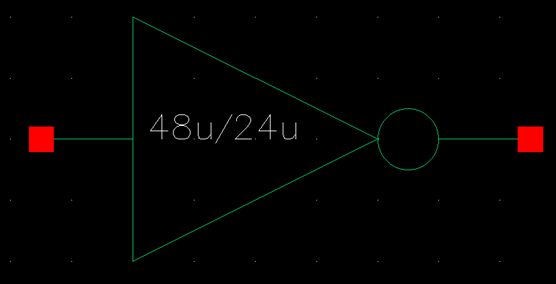
Internal schematic for the inverter Inverter
symbol created
Layout of 48u/24u
inverter (with verification):
|
Inverter
layout |
Inverter layout extracted view |
DRC and LVS verification |

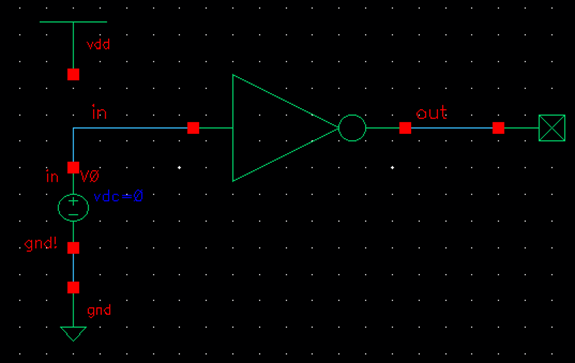
12u/6u Inverter SPICE
Simulations
The following snip
shows the schematic that I drafted to simulate the results of different
capacitive loads on the 12u/6u inverters output.
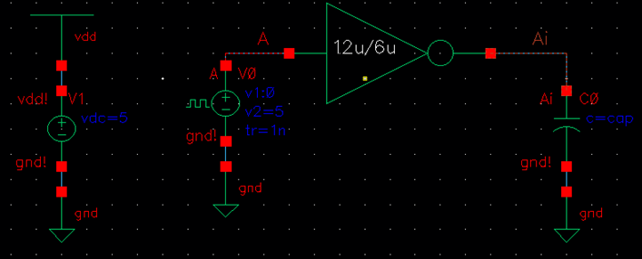
This lab required use
of both Spectre and UltraSim
SPICE simulators. UltraSim is faster than Spectre and therefore useful for larger circuits. The
faster speed comes at the cost of accuracy. Since this is a relatively
small circuit, the difference in accuracy goes mostly unnoticed.
Transient using Spectre Transient using UltraSim
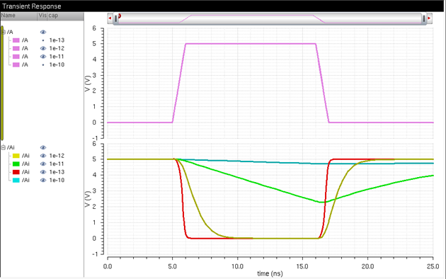
As stated previously,
we expect an inverter to output high when its input is low, and output low when
its input is high. The different output waves created under different capacitor
loads shown here can be explained using knowledge of the basic operation of a
capacitor. As the capacitor load value is increased, the time it takes for it
to charge and discharge also increases. The 100fF and 1pF loads perform
correctly. However, the 10pF load is on the boarder of high and low
(unreliable) and the 100pF load is outputting high, meaning that this inverter
cannot handle loads of 10pF or greater.
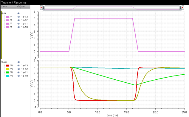
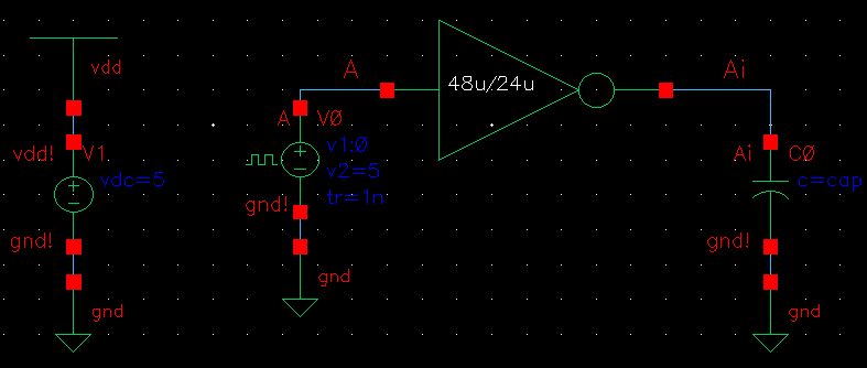
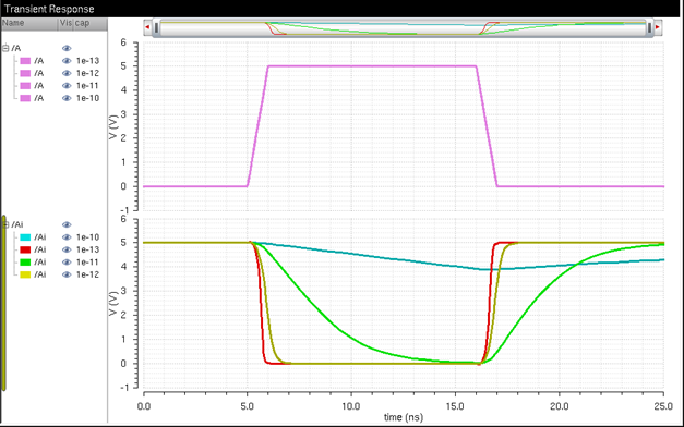
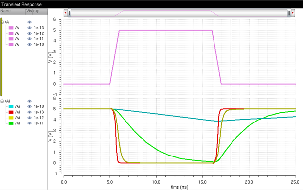
48u/24u Inverter SPICE
Simulations
The
following snip shows the schematic that I drafted to simulate the results of
different capacitive loads on the 48u/24u inverters output.
Transient using Spectre Transient Using UltraSim
The most noticeable difference
that occurs in output when making the inverter bigger is that it can handle
capacitive loads better. To be more specific, the outputs shown here have the
same load values has the outputs shown above for the smaller inverter, but this
one is performing better. The 100fF and 1pF load outputs are responding
correctly to the inputs in a smaller amount of time. Additionally, the 10pF
capacitor is outputting the correct value (low), which contrasts the smaller
design. So, this inverter can perform correctly with a load that is one order
of magnitude greater than the smaller inverter (10pF).
The last step I took in this lab was backing up all my work to my
Google Drive, as shown in all previous labs. This concludes the lab.