Lab 4 - EE
421L
Email: boloor@unlv.nevada.edu
Prelab:
Back-up
all of your work from the lab and the course.
- Read
through this lab before starting it.
- Go
through Tutorial 2
seen here.
- In
the simulations in this lab the body of all NMOS devices (the substrate)
should be at ground (gnd!) and the body of all
PMOS devices (the n-well) should be at a vdd! of
5V.
Tutorial two walks through how to
create the schematic and layout of an NMOS and PMOS transistor, as well as how
to create their corresponding IV curves.
The following
images show the layout of my NMOS (left) and PMOS (right):
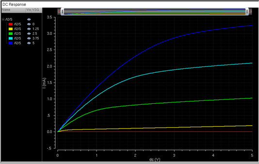
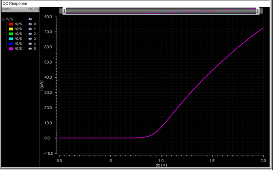
The next images show the IV curves that the extracted views of these
transistors create. The NMOS on the left and the PMOS on the right. They check
out as the correct VGS/VSG IV curves.
- Generate
4 schematics and simulations (see the examples in the Ch6_IC61 library, but note that for the PMOS body should be at vdd! instead of gnd!):
- A schematic for simulating ID v. VDS of an NMOS
device for VGS varying from 0 to 5 V in 1 V steps while VDS varies from 0
to 5 V in 1 mV steps. Use a 6u/600n width-to-length ratio.
- A schematic for simulating ID v. VGS of an NMOS device
for VDS = 100 mV where VGS varies from 0 to 2 V in 1 mV steps. Again use a 6u/600n width-to-length ratio.
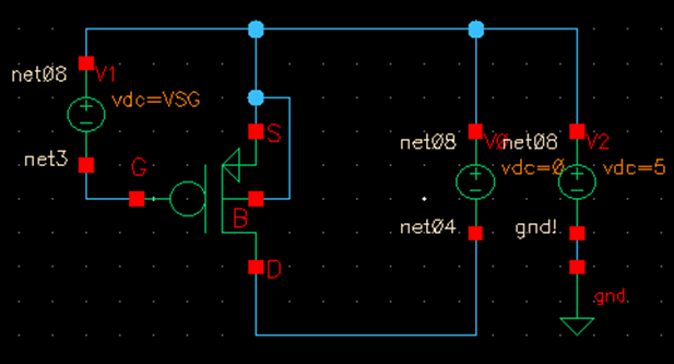
- A schematic for simulating ID v. VSD (note VSD not VDS)
of a PMOS device for VSG (not VGS) varying from 0 to 5 V in 1 V steps
while VSD varies from 0 to 5 V in 1 mV steps. Use a 12u/600n
width-to-length ratio.
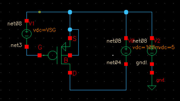
- A schematic for simulating ID v. VSG of a PMOS device
for VSD = 100 mV where VSG varies from 0 to 2 V in 1 mV steps. Again, use
a 12u/600n width-to-length ratio.
- Lay
out a 6u/0.6u NMOS device and connect all 4 MOSFET terminals to probe pads
(which can be considerably smaller than bond pads [see MOSIS design rules] and directly
adjacent to the MOSFET (so the layout is relative small).
- Show your layout passes DRCs.
- Make a corresponding schematic so you can LVS your
layout.
- Lay
out a 12u/0.6u PMOS device and connect all 4 MOSFET terminals to probe
pads.
- Show your layout passes DRCs.
- Make a corresponding schematic so you can LVS your
layout.
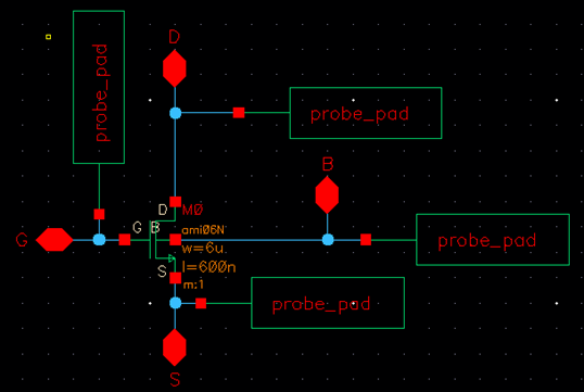
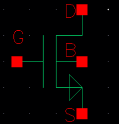
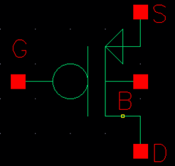
To begin, I made schematics and symbols for the NMOS and PMOS
with probe pads, shown below. I made these according to the design parameters –
the NMOS is 6u/600 and the PMOS is 12u/600 width to length.
![]()
![]()
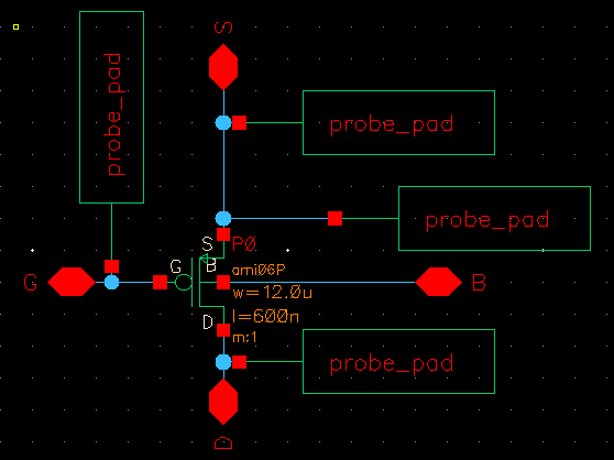
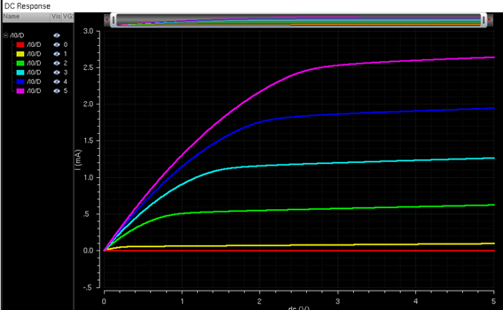
Schematics and Simulations to Test the NMOS and PMOS
Note
that the first two simulations are NMOS transistors that use a 6u/600n
width-to-length ratio, and the last two simulations are PMOS transistors that
use a 12u/600n
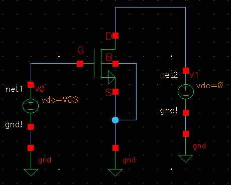
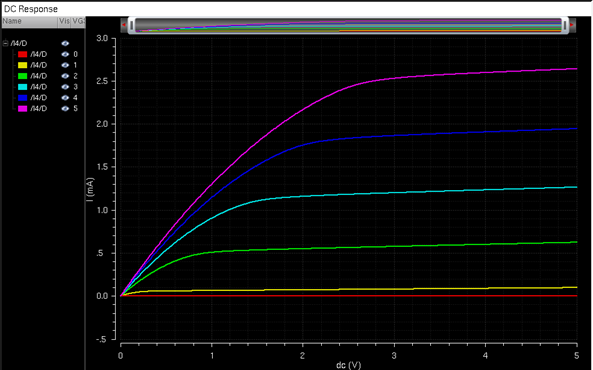
A schematic for
simulating ID v. VDS of an NMOS device for VGS varying from 0 to 5 V in 1
V steps while VDS varies from 0 to 5 V in 1 mV steps:
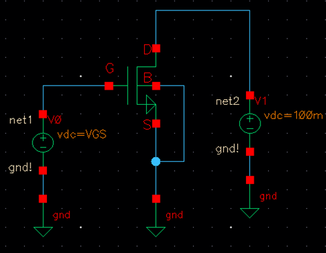
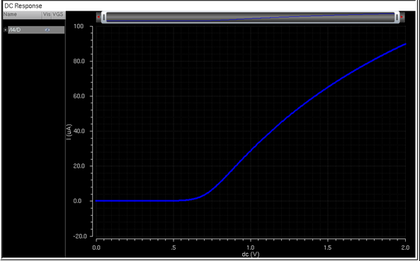
A schematic for
simulating ID v. VGS of an NMOS device for VDS = 100 mV where VGS varies from 0
to 2 V in 1 mV steps:
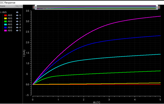
A schematic for
simulating ID v. VSD (note VSD not VDS) of a PMOS device for VSG (not VGS)
varying from 0 to 5 V in 1 V steps while VSD varies from 0 to 5 V in 1 mV
steps:
A schematic for
simulating ID v. VSG of a PMOS device for VSD = 100 mV where VSG varies from 0
to 2 V in 1 mV steps:
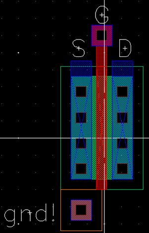
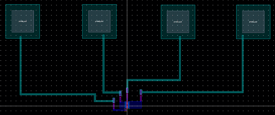
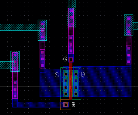
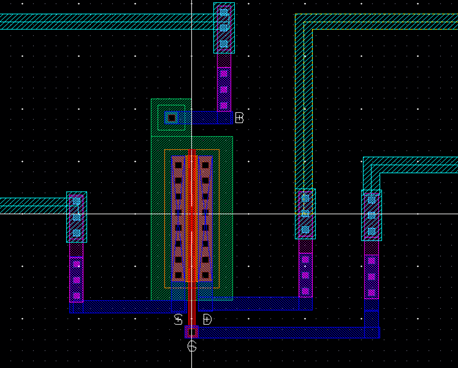
Layout of a 6u/0.6u NMOS Device with Probe Pads
Next, I created a layout for the NMOS
and PMOS with probe pads. These layouts were made by connecting the metal1
layer of the drain, gate, source, and body to metal2 using vias. These are then
connected to metal3 (again, using vias), which connects to the layer the pads
are on.
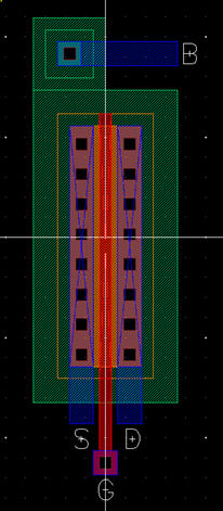
The following images
show the full layout of the NMOS as well as a zoomed in version without the
pads:
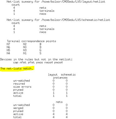
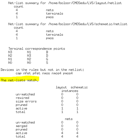
Proof that the NMOS design passes DRC and LVS verifications:
DRC:
![]()
LVS (compared to schematic with pads):
Layout of a 6u/0.6u NMOS Device with Probe Pads
The following images show
the full layout of the PMOS as well as a zoomed in version without the pads:
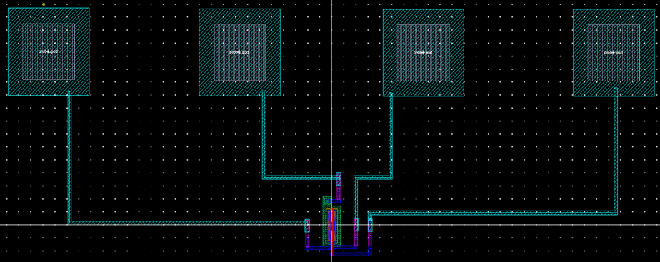
Proof that the PMOS
design passes DRC and LVS verifications:
DRC:
![]()
LVS (compared to schematic with pads):
This concludes the lab work.