Final Project – Design, Simulation, and Layout of a Times Four (x4)
Clock Multiplier
EE 421L Digital IC Design
Schematics Due: 11/13/19 at 11:30am
Layout and Documentation Due: 11/20/19 at
11:30am
Last Edited on
11/19/19 at 10:23pm using Word
Go To Simulations Using The
Current Starved Inverters…
Go To How to Improve Initial
Design…
Go To Part II – Layout of the Times
Four (x4) Clock Multiplier
Click here to see the final layout.
Click here to
download EE421L_FinalProject.zip
For this
project, a circuit will need to be designed to take in a 9-11 MHz input clock
signal and generate a frequency between 36-44 MHz clock signal.
This circuit
is a x4 Multiplier, where the output clock frequency is the input clock
frequency multiplied by 4.
For simplification,
the input clock will have a 50% duty cycle.
How are we
able to generate a pulse that is faster than our input?
For this, we
will look at an XOR gate.
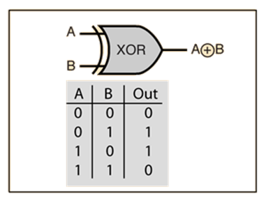
Figure 1, An XOR gate, with Truth
Table
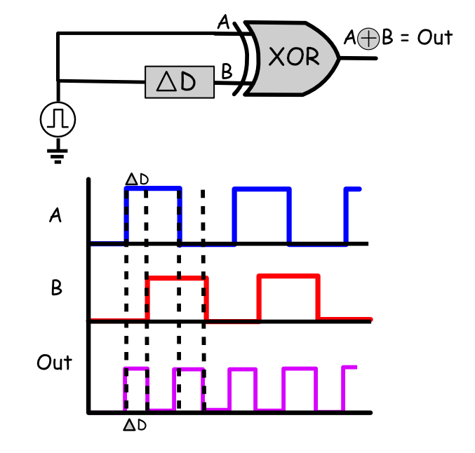
Figure 2, A Representation of how the
frequency can be doubled using an XOR gate.
If we get a
genuinely nice delay ΔD, we can then use the XOR gate to generate a pulse
that is double the input frequency (since the XOR only outputs during a
rise/falling edge of the input signal, and there are 2 of these events every
period, or 2/T = 2ƒ).
After we get
this doubled frequency, we will then use the output in another XOR gate to
double the doubled-input frequency (so times 4).
--------------------------------------------------------
Part I: Schematics and Design
Discussions
To multiply
the frequency by four, we will first look at how to multiply the input
frequency by two using the XOR gate.
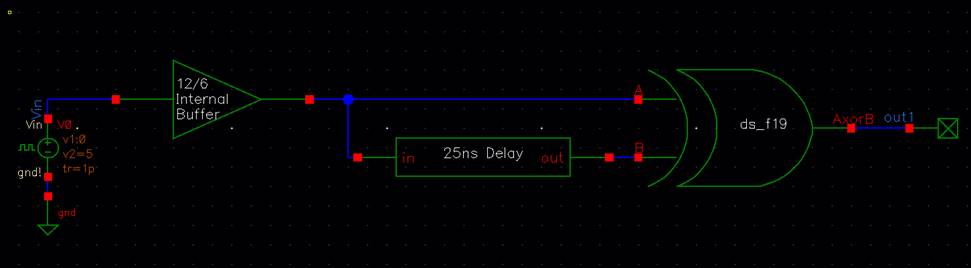
Figure 3, the first stage x2
Multiplier
Note, the
reason for the beginning buffer is so that just in case the rise time of the
input is not fast enough, we can buff the incoming signal so that it can be
processed into the XOR gate and delay.
The buffer in
the beginning are two 12u/6u inverters.
We will be
designing at an input frequency of 10 MHz (a period of 100ns or a 50ns/50ns
duty cycle).
The delay of
the 2nd input of the XOR gate should be around 25ns.
Here is the
delay block:
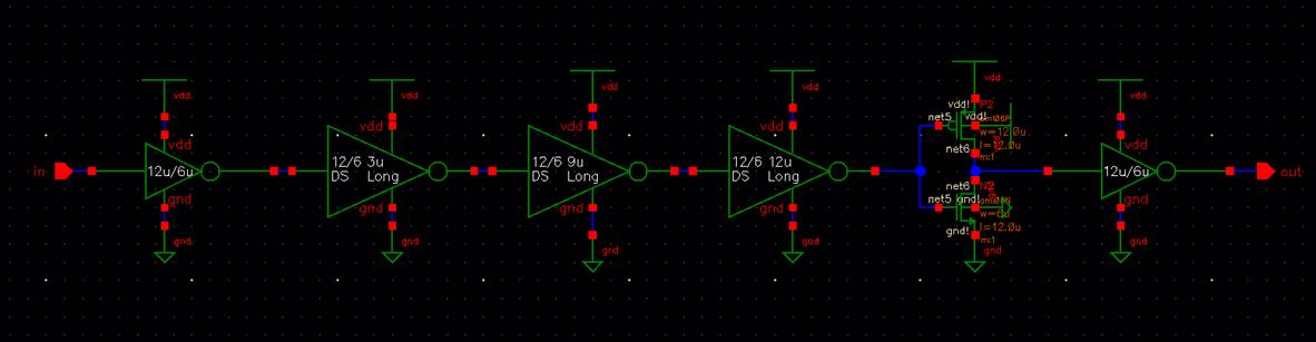
Figure 4, the Delay block that will
delay the input by around 25ns.
For this, we begin
with one 12u/6u inverter (using minimum length), and we have 4 long inverters,
with each inverter having a longer length than the previous inverter.
I chose this
progression because of how the input capacitance was affecting each inverter. I
made it to where the larger lengths were first, but then the RC delay length of
the signal would be cut down tremendously, and thus there was too much
capacitance at the beginning stage. With this topology, each stage will have a
steady increase of total capacitances so that we can propagate the full length
of the signal.
Schematic of
the first long inverter:
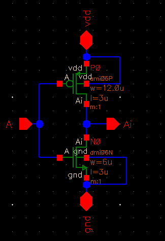
Figure 5, Schematic of a Long Inverter
- 12u/6u, Length of 3u
Idea of the
total capacitances:
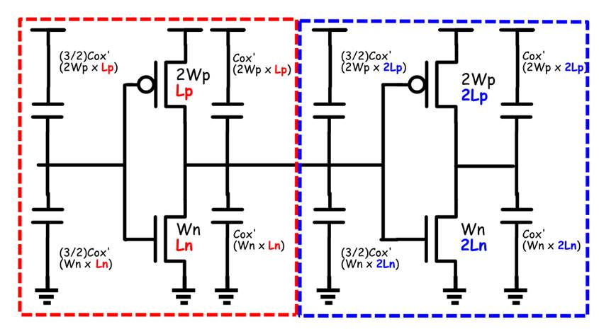
Figure 6, The Capacitances of the Long
Inverters.
In Figure 6,
as you can see, as we increase the length of L, we also increase the
capacitance of both the input and output of the long inverter.
This is why I placed a small “pre-buffer” at the beginning of
the delay, so that this capacitance does not affect the first
input of the XOR gate.
Also, with
increasing the length, the effective resistances of the long inverters
increase.
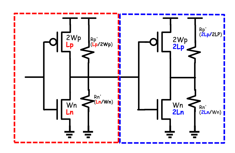
Figure 7, The Effective Resistances of
the Long Inverters.
Changing the
lengths will surely increase the capacitances, thus having a longer delay as
the signal propagates from one inverter to the next. However, the effective
resistance goes up, which will also increase delay, but will change the
strength of the MOSFETs to where the actual length of the input will change.
This topology of using a few long length inverters instead of a bunch of
regular 12/6 inverters will save on layout, however we
will need to then consider the RC delays of both the PMOS and NMOS and design
to where there is an equal amount of delay for when either MOSFET is turned on.
Looking at the
end of the delay:
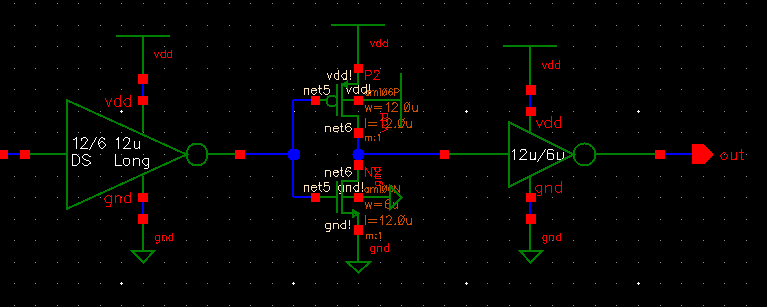
Figure 8, an Inverter with no symbol,
followed by a regular 12/6 inverter
We have an
inverter with no symbol. This is used so that we can finely tune our delay to
whatever we need it to be.
The inverter
at the end is used to buff up the signal, and so that the output as a small
output capacitance so that it can be used to feed into the input of the XOR
gate.
Output of the first XOR Gate,
input 1 (Red), Delayed input 2 (Green), Doubled frequency output (Orange)
Now, lets look
at the output of the first XOR gate with this delay block:
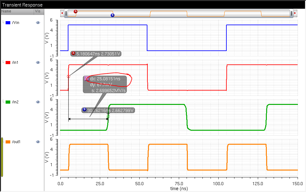
Figure 9, the Output of the XOR gate (Orange), and showing Input 1 (Red) and delayed Input 2 (Green).
This shows
that our XOR gate is doubling the frequency. Now, we will use this output of
the XOR gate to feed into another XOR gate.
Below we have
the following circuit:
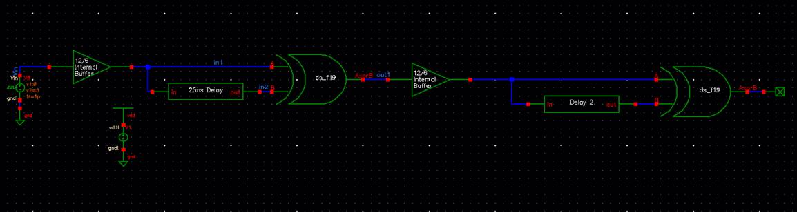
Figure 10, the x4 Frequency Multiplier
Circuit
The output of
the first XOR gate will feed into a 12/6 buffer, similar to
what we had in the beginning of the circuit so that our first XOR gate can
process the signal.
By analogy, we
can think of the 2nd stage XOR as the 1st stage XOR but
with a different input frequency:
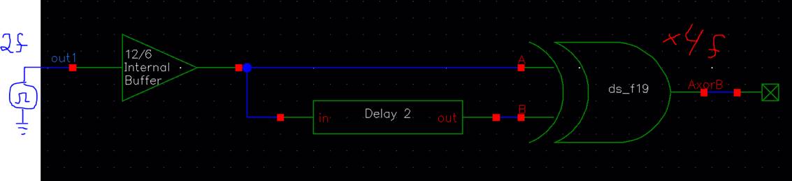
Figure 11, Simple view of the 2nd
Stage XOR Gate. Note its similarity to the 1st Stage XOR Gate.
The output of
Stage 1 is a 20 MHz signal (50ns or 25ns/25ns Duty Cycle). Therefore, our 2nd
delay should be around 12.5ns.
Here is the 2nd
delay:
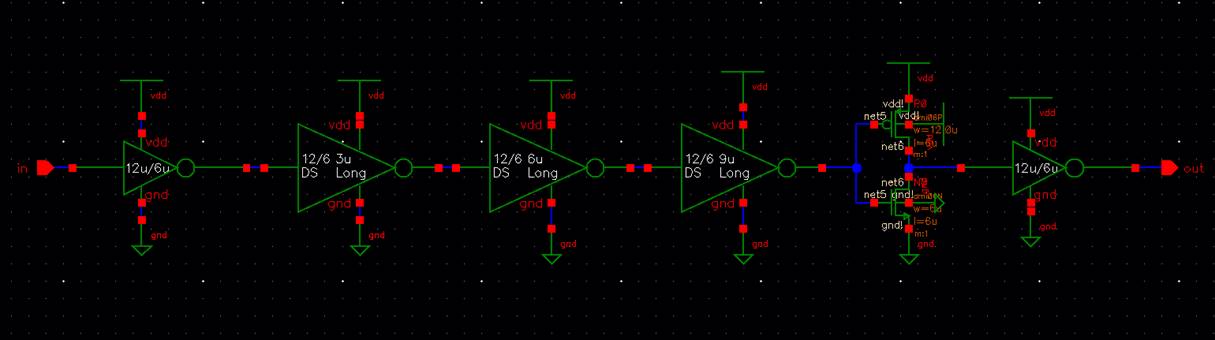
Figure 12, The 2nd Delay
block. Note its similarity to the first delay block, but with a different
Length size.
In this delay
block, we have a similar topology to that of the first delay block, but the
lengths are smaller and do not increase dramatically as the first delay.
We could have
implemented less inverters with larger lengths, but then our RC time constant
will be much slower in the middle and the input signal will not propagate fully
into the circuit and the output signal will not be a 50/50 duty cycle.
Output of the second XOR Gate,
input 1 (Red), Delayed input 2 (Green), Doubled frequency output (Dark Red)
Looking at the
output of the 2nd XOR Gate:
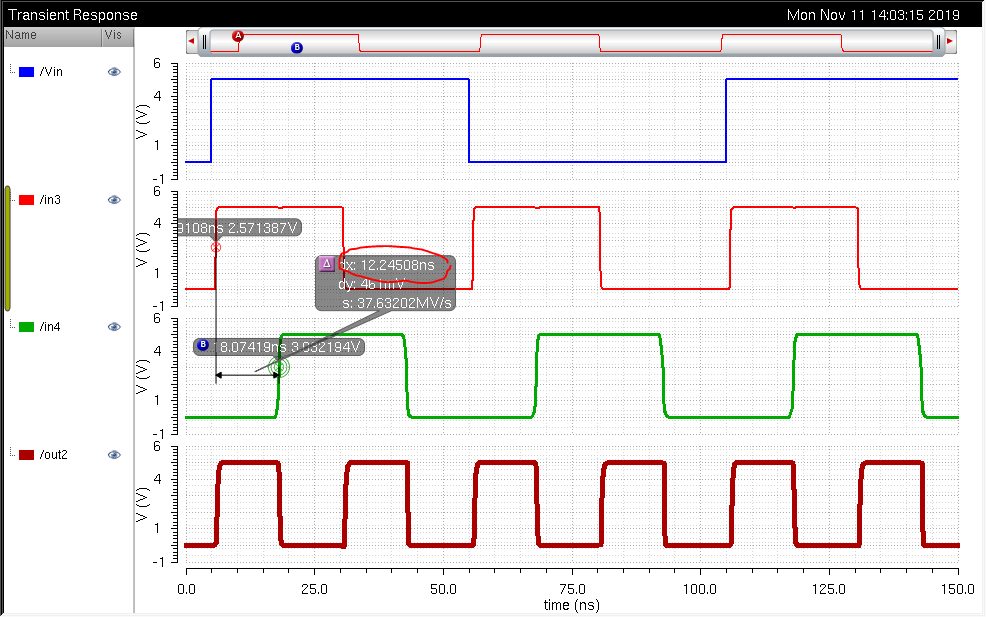
Figure 13, The Output of the 2nd
XOR gate (Dark Red), with Input 1 (Red) and the delayed Input 2 (Green).
Here, we can
see that we get our delay, and therefore, our XOR gate is doubling the doubled
input frequency (so x4).
Creating a
cell view for our x4 frequency multiplier:
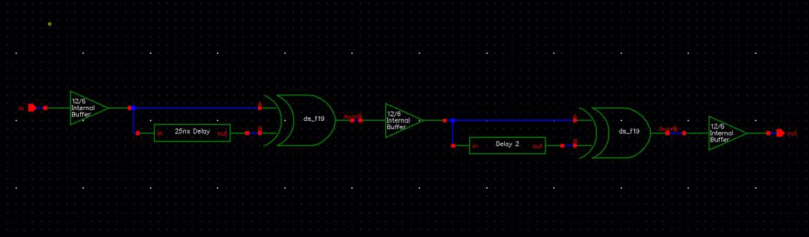
Figure 14, The x4 Frequency Multiplier
Schematic View

Figure 15, The x4 Frequency Multiplier
Symbol View
---------------------------------------------------------------------------------------------------
Here is the
following simulation circuit:
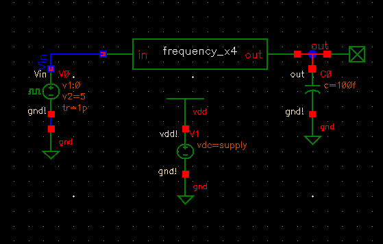
Figure 16, The x4 Frequency Simulation
Circuit
Input Frequencies at Different
VDD Power Supply Voltages:
Testing at
different input frequencies and using the Parametric Analysis Tool to change
our voltage supply in the ADE:
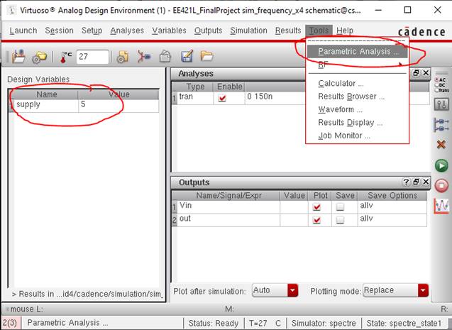
Figure 17, my ADE Setup
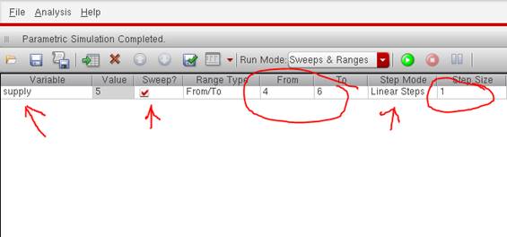
Figure 18, Using the Parametric
Analysis Tool
9MHz:
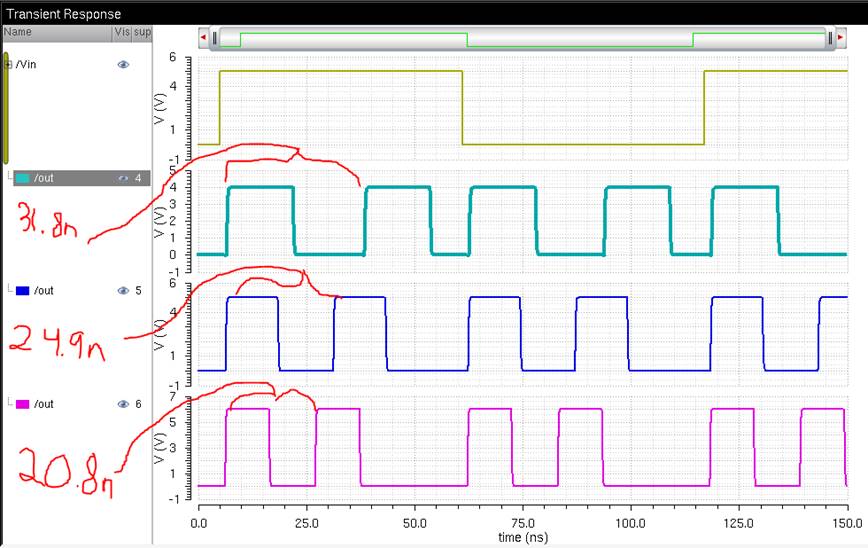
Figure 19, Input Frequency = 9 MHz,
With changing Voltage Supply (4V Turquois, 5V Blue, 6V Magenta)
10MHz:
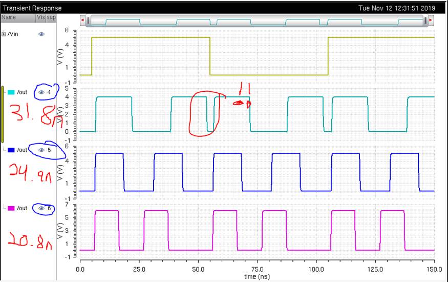
Figure 20, Input Frequency = 10 MHz,
With changing Voltage Supply (4V Turquois, 5V Blue, 6V Magenta)
11 MHz:
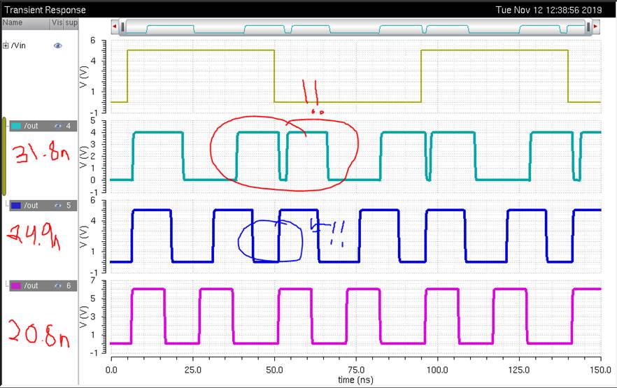
Figure 21, Input Frequency = 11 MHz,
With changing Voltage Supply (4V Turquois, 5V Blue, 6V Magenta)
|
Input
Frequency = 9MHz |
4V |
5V (Ideal) |
6V |
|
9 MHz
(110ns) |
31.4 MHz |
40.1 MHz |
48.1 MHz |
|
10 MHz
(100ns) |
31.4 MHz |
40.1 MHz |
48.1 MHz |
|
11 MHz
(90ns) |
31.4 MHz |
40.1 MHz |
48.1 MHz |
Looking at
this, as the voltage supply voltage changes from 4V to 6V, with lower supply
voltages, we get a “slower” frequency at the output of our x4 frequency multiplier.
This is due to having less current flowing from VDD! to GND! With the supply
voltage at 4V (Turquois), our output
is at a “lower” frequency, but if the input frequency is too fast, the signal
overlaps to the next period of the input frequency.
With the
supply voltage at 6V, our output is a “higher” frequency (Magenta), but at lower frequencies, you see
that we do not have a good duty cycle.
At the nominal
voltage of 5V (Blue), the signals
are sitting at a good middle ground of 40.1 MHz.
Before we
proceed, we have a problem.
The delays are
NOT a function of our input
frequency.
For this, we
will want a delay that can change depending on what our input frequency is.
---------------------------------------------------------------------------------------
How to Improve our Initial Design:
Suppose we
modify the delays to have a Current Staved Inverter.
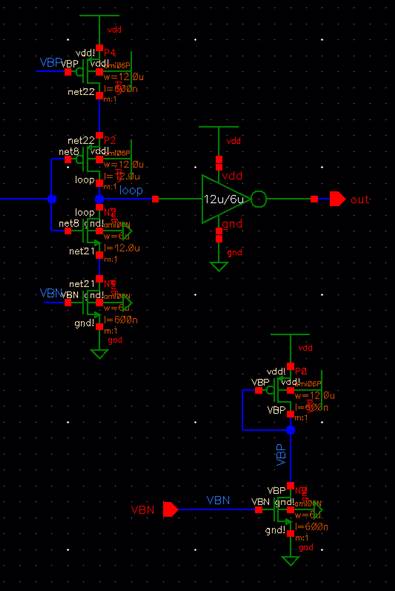
Figure 22, Modifying the first delay
block with Current-Starved Inverters
A Current
Starved Inverter is basically an inverter, but the current from VDD! to GND! is
limited, or “starved”, and the current in the inverter will change, thus
changing the delay.
If there is
little current in the inverter, then the circuit behaves as if there is less
power, therefore, the inverters gets slow.
If there is
lots of current in the inverter, the circuit may just behave as a regular
inverter.
Here is a
quick figure of the Current Starved Inverter:
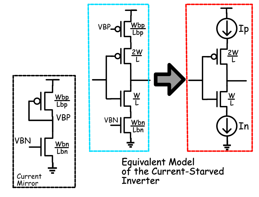
Figure 23, The Current Starved
Inverter Equivalent Model
For this, we
have a small current-mirror that will take in a bias voltage, VBN, for the NMOS
and output a bias voltage, VBP for the PMOS and these will drive the current
mirrors above and below the inverter.
We will then
modify our frequency multiplier and delay blocks so that they will have this
new bias voltage input.
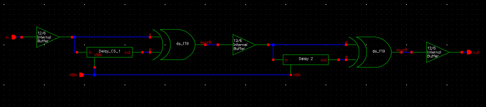
Figure 24, Modifying the Frequency
Multiplier with voltage-controlled Delays.
The 2nd
delay block will be designed to take in the same bias voltage as the first
delay block.
Delay 1 Simulation: Input Frequency
At 10 MHz, Sweeping VBN
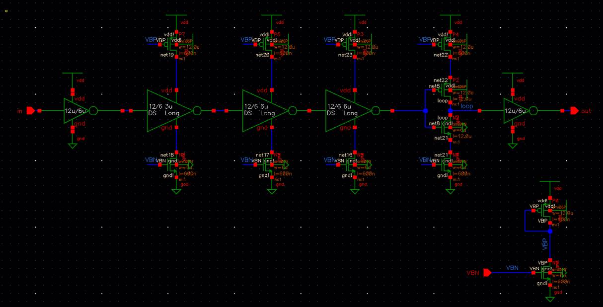
Figure 25, Delay Block 1 with current
starved Inverters
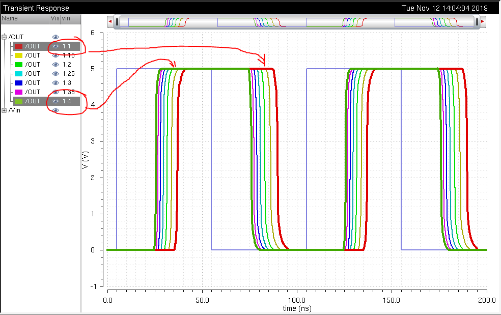
Figure 26, Looking at the delays as
the input bias voltage sweeps from 1.1V to 1.4V.
From this we
can say as we sweep the bias voltage, we get larger delays with lower VBN (aka,
the inverter is being “starved” of current).
From 1.1V to
1.4V, we will be ok if we have our bias voltage swing +/-100mV. We will then
design so that our bias voltage is high so we can have a linear bias input
voltage.
By analogy, we
will also do the same with the 2nd delay block but considering that
we will take in the same high input voltage as used in delay block 1.
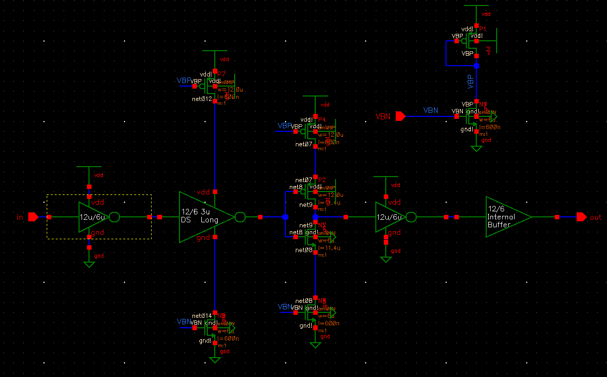
Figure 27, Delay Block 2 with
Current-Starved Inverters
Question: Where do I connect
the body of the NMOS and PMOS of the Current-Starved Inverters?
For this
special case, we will tie the body of the PMOS to the Source of the PMOS, and
the body of the NMOS to the Source of the NMOS.
This will then
reduce the Source-Body effect, and our Threshold Voltage will stay relatively
low. We could connect the bodies of the PMOS and NMOS to VDD! and GND!, respectively, but then the Threshold Voltage will
increase and we can run at a possibility that the inverters will switch on
correctly.
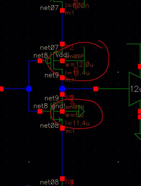
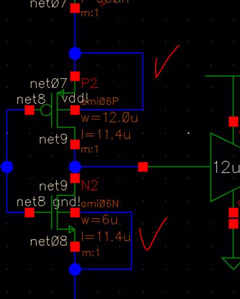
Figure 28 and 29, Connecting the bodies
of the PMOS and NMOS to their respective Sources.
Simulation with The Current-Starved Inverters:
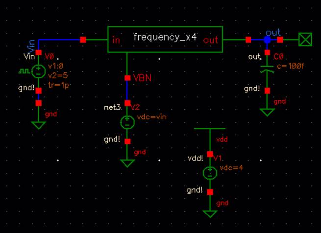
Figure 30, The x4 Frequency Multiplier
with the Current-Starved Inverters.
9 MHz: VBN =
1.15V
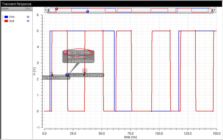
Figure 31, Sim Showing Current Starved
Inverters, Delay ≈ 14.4ns
10 MHz: VBN =
1.25V
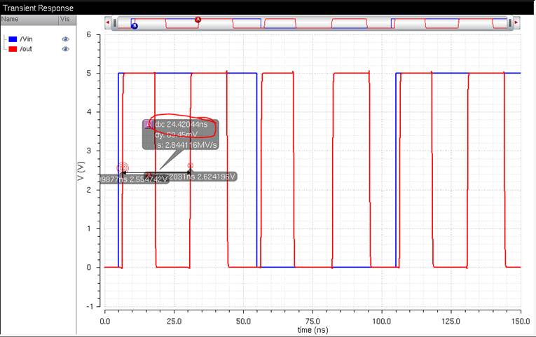
Figure 32, Sim Showing Current
Starved Inverters, Delay ≈ 12.3ns
11 MHz: VBN =
1.35V
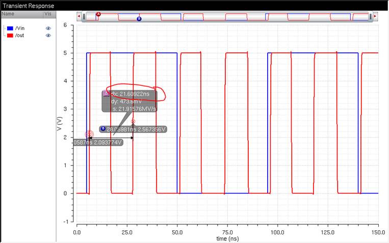
Figure 33, Sim Showing Current Starved
Inverters, Delay ≈ 7.2ns
For The Supply Voltage = 5V (Ideal)
|
Bias Voltage
VBN |
Input
Frequency |
Output
Frequency |
Delay |
|
1.15V |
9 MHz |
34.8 MHz |
14.4ns |
|
1.25V |
10 MHz |
40.9 MHz |
12.3ns |
|
1.35V |
11 MHz |
46.3 MHz |
7.2ns |
This shows that
the Current Starved Inverters work and are changing the delays so that we can
try to have a 50% duty cycle.
Changing the Power Supply:
For the change
in power supply (And using the same Bias Voltages from above):
9 MHz (110ns
period): VBN = 1.15V
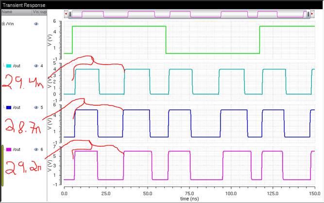
Figure 34, Input Frequency = 9 MHz,
Voltage Supply (4V Turquois, 5V Blue, 6V Magenta), Using Current Starved (CS) Inverters
10 MHz (100ns
period): VBN = 1.25V
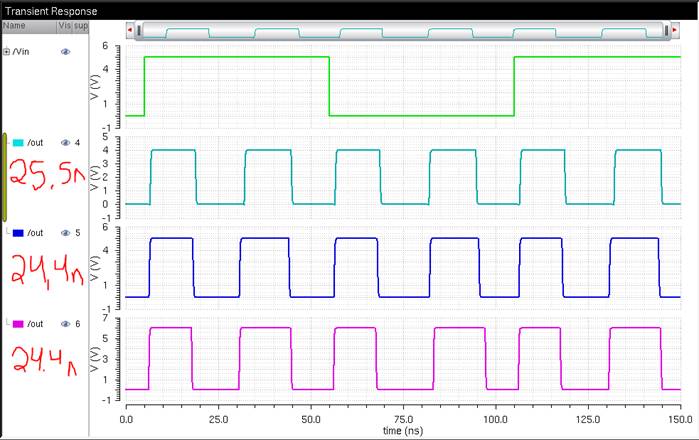
Figure 35, Input Frequency = 10 MHz,
Voltage Supply (4V Turquois, 5V Blue, 6V Magenta), With CS Inverters
11 MHz (90ns period):
VBN = 1.35V
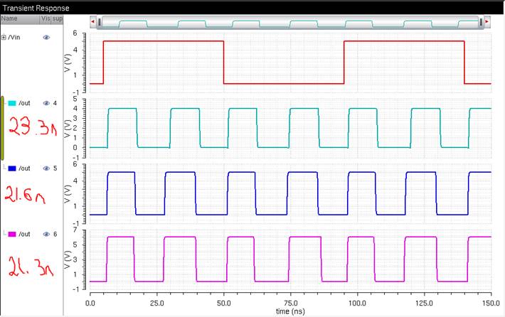
Figure 36, Input Frequency = 11 MHz,
Voltage Supply (4V Turquois, 5V Blue, 6V Magenta), With CS Inverters
|
Input Frequency |
Bias Voltage |
Supply
Voltage |
||
|
VBN |
4V |
5V |
6V |
|
|
9 MHz
(110ns) |
1.15V |
34 MHz |
34.8 MHz |
34.2 MHz |
|
10 MHz
(100ns) |
1.25V |
39.2 MHz |
40.9 MHz |
40.9 MHz |
|
11 MHz
(90ns) |
1.35V |
42.9 MHz |
46.2 MHz |
46.9 MHz |
This finally
concludes that the Current-Starved Inverters are changing the delays, and
consequently the output frequency.
Conclusions Part I:
The XOR gate can
be used to double the input frequency by taking the input signal and XOR the
signal with a delayed version of itself.
Using the
delays of the inverters can help with a specific frequency, however, these
delays are constant with different input frequencies.
A Change in
the power supply with a regular inverter delay can keep delays consistent, but
even with a different constant voltage supply, the delays will be constant with
different input frequencies.
The Current-Starved
Inverter is one take at changing the delays by “starving” the delay inverters
of current, consequently slowing down the inverter.
The negative
of this approach is you will need double the transistors, thus, using more
power. Also, the input bias voltage will output nonlinear delays.
There is a
discussion found in Chapter 19 of CMOS – Circuit Design, Layout, and
Simulations – 4th Edition regarding linearizing the current, and
thus linearizing the delays.
Here is a
quick figure on how to linearize the current in the CS Inverter:
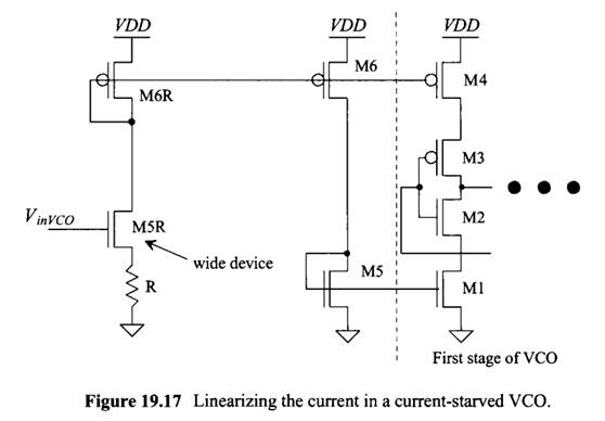
Figure 37
Based on the
Square-Law, the Current is a function of the square of VGS.
Looking at
M5R, if made much wider compared to the rest of the circuit, the VGS will be
more independent of the Input Bias Voltage and more on Vthn.
This will then
try to linearize the current in our current mirror and thus, the delays could
be linear with respect to the Input Bias Voltage.
This concludes
Part I of the Final Lab Project.
------------------------------------------------------------------
Part II: Layout of the Times
Four (x4) Clock Multiplier
For this design,
we will stick with our Current Starved Inverters in our final layout design.
Note! Please, if you are a future student
reading this, the biggest tip is to create a cellview
for everything, even a small NMOS connected to VDD!
We will have
the following circuit:
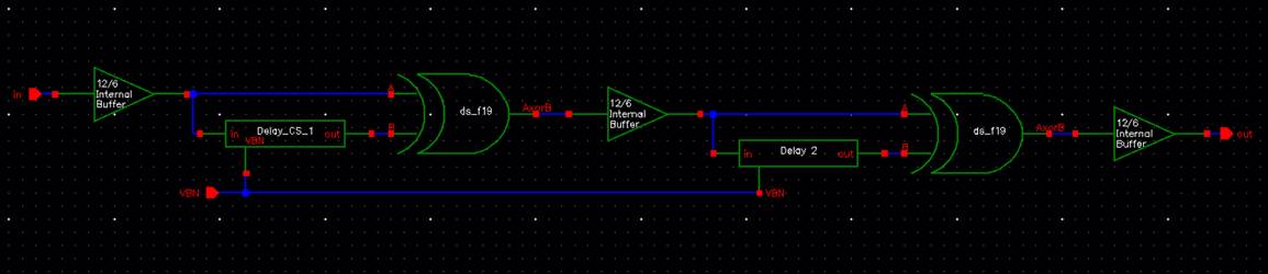
Figure 38, The Times Four (x4) Clock
Multiplier
However, for simplicity
and to make Layout-to-Schematic verification easier, we will have the following
simple circuit:
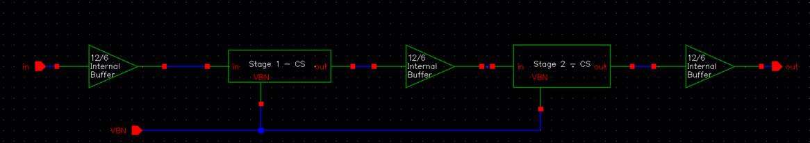
Figure 39, The Times Four (x4) Clock
Multiplier, Simple View
In this schematic,
every block has a single input, therefore, the final layout will be very
simple.
Here is Stage
1, using Current Starved Inverters:
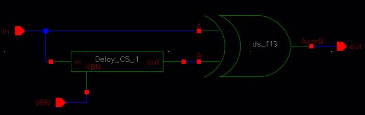
Figure 40, The First Stage Block
Schematic
The layout for
this circuit will be complicated, but will be much
easier to debug since we are focusing on just this section, and not an entire circuit.
Symbol of the
first delay block:
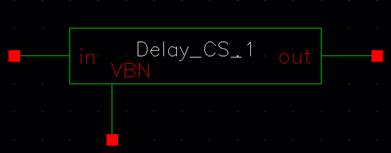
Figure 41, The First Delay Block, with
Current Starved Inverters, Symbol View
Here is the
layout of the first delay block, using Current Starved Inverters:
Figure 42, The Layout of the First
Delay Block Using Current Starved Inverters, High
Resolution x5 (Click on Image or “High Resolution x5 for Higher Resolution)
We made the
gap in between the PMOS (top) and NMOS (bottom) big so that we can plan ahead for future layouts.
The lighter
pink 1x3 rectangles connecting the gates of the L = 600nm CMOS devices are the
gates of the current mirrors.
The Long L Devices
are the big red rectangles.
The input pin
is “in”, output pin is “out”, the input bias voltage pin for the current
mirrors is “VBN”. All pins are on metal 1.
Question: Why am I not connecting
the bodies of the Long Length Inverters to their sources?
To change the
potential of the body of a PMOS, consider the following:
Figure 43, Long Length PMOS with
different body potential
This is our
Long Length Device with a different body potential.
As shown, the
N-Wells will be at different potentials and will need to be separated a certain
distance.
This will then
make our overall layout much larger than it should be and wastes space.
Using a
Source-Body PMOS will reduce the body effect, but will
use lots of layout.
Having the
N-Well connected to VDD! will add a body effect, but
can be considered negligible.
Now, we can
use this delay block to connect to our XOR gate.
Here is the
first stage block of our x4 clock multiplier:
Figure 44, The First Stage Block,
Symbol View
Here is the
Layout of the First Stage Block:
Figure 45, The First Stage Block
Layout View, High Resolution x4
In the
beginning is our delay block. The XOR gate is at the far right of the layout
(smaller PMOS device).
There is a metal
2 wire from the beginning of the delay all the way to the first input of the
XOR gate.
The second
input of the XOR gate comes from the output of the delay block.
The input bias
voltage pin is called “VBN”. Note, VBN is a pin that will always need to be
wired.
Verification of the First
Stage:
So usually
there will be Design Rule Checks (DRCs) and Layout-To-Schematic (LVS) tests.
All cellviews discussed previously have passed both DRC and
LVS.
We will do a big
DRC and LVS check for the first stage (just to make sure the first half of the
circuit works).
DRC of the
First Stage Block:
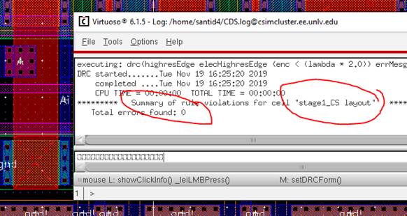
Figure 46, DRC of the First Stage
Block, Passes DRC
Extracted:
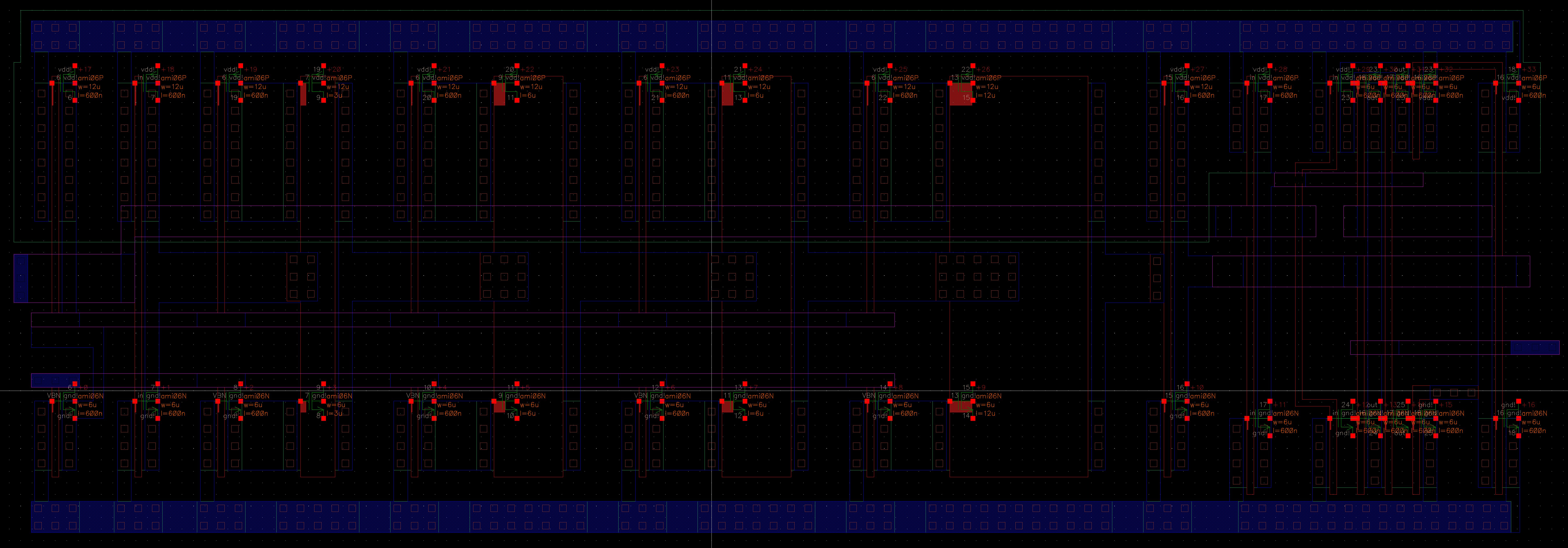
Figure 47, Extracted View of the First
Stage Block, High Resolution x5
LVS:
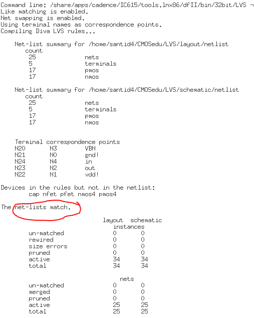
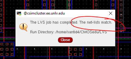
Figure 48 and 49, LVS Output file and LVS Passing.
From this,
since this first stage passed all DRC and LVS verifications, all cell views
used within the first stage should passively pass all tests.
Moving on to
the Second Stage Block:
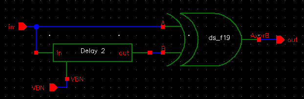
Figure 50, Second Stage Block
Schematic
Now, Looking
at the second delay, with Current Starved Inverters:
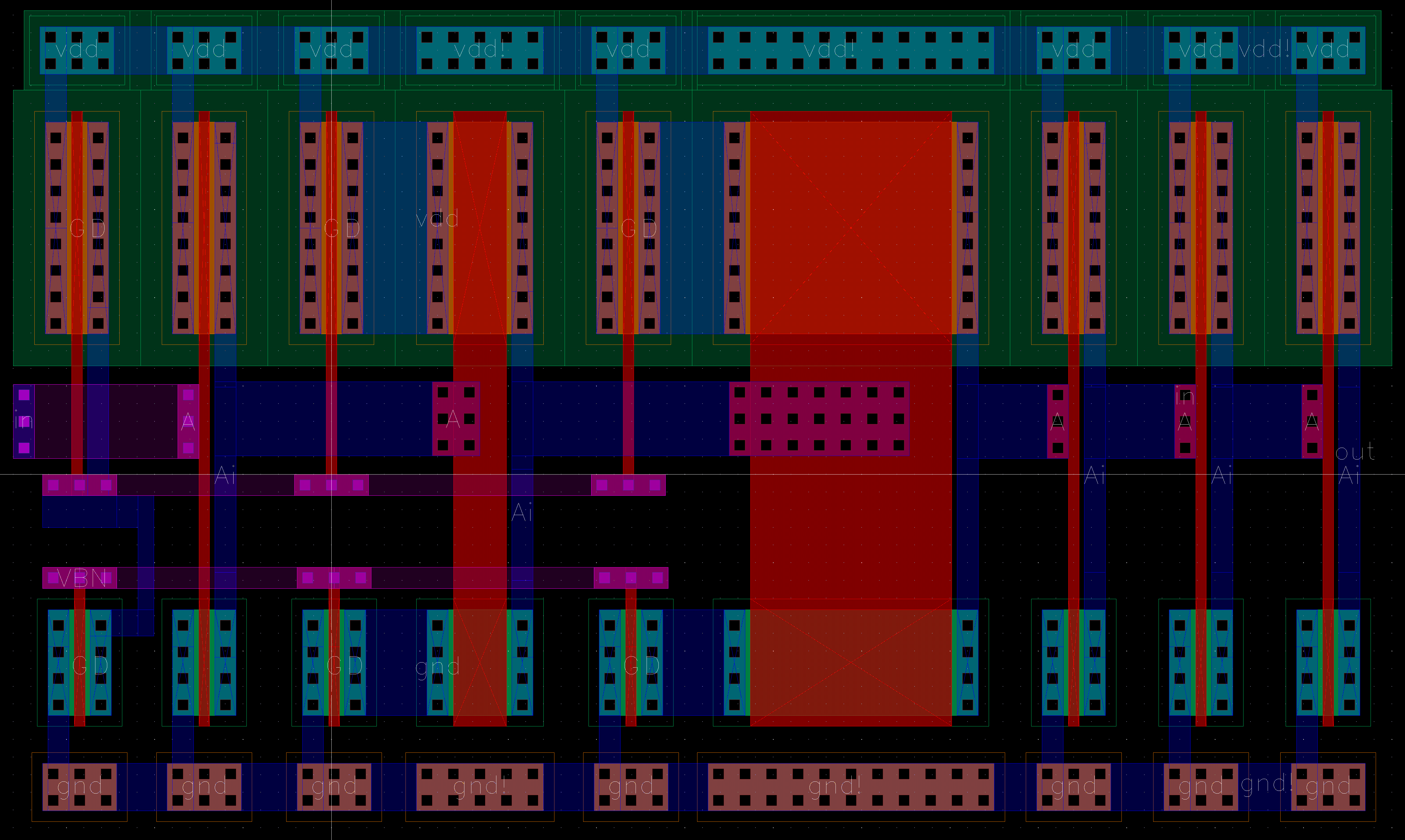
Figure 51, The Second Delay Block,
With Current Starved Inverters, Layout View, High
Resolution x4
Symbol View:
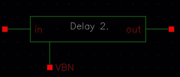
Figure 52, The Second Delay Block,
With Current Starved Inverters, Symbol View
Here is the
Second Stage Layout:
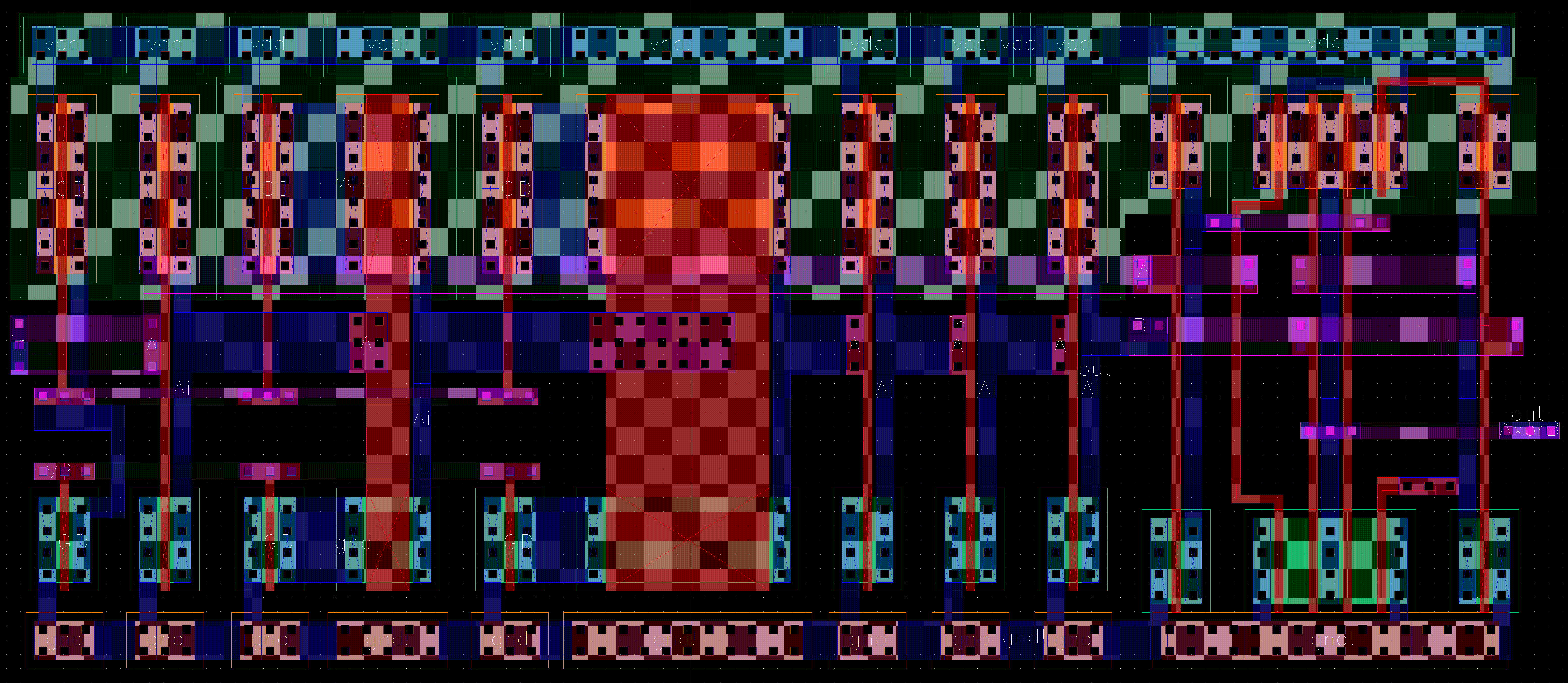
Figure 53, The Second Stage Block,
With Current Starved Inverters, Layout View, High
Resolution x4
Note that it
looks similar to the First Stage Block.
The Input pin
is “in”. The Output Pin is “out”. The Input Bias Voltage Pin (Center Left) is
“VBN”.
Yes, we can
label the pins the same names as other blocks. Instantiating these blocks will
ignore the pins.
Symbol View:
Figure 54, The Second Stage Block,
With Current Starved Inverters, Symbol View.
Now that
everything has been designed, lets put it all together.
Revisiting our
simple Times Four (x4) Clock Multiplier:
Figure 55, The Times Four (x4) Clock
Multiplier, Schematic View, High Resolution
x4
Since
everything has been created (the buffers and stages), it will be very easy to
connect everything together.
Layout View Of the Times Four (x4) Clock Multiplier:
Figure 56, The Times Four (x4) Clock
Multiplier, Layout View, High Resolution x6
Symbol View:
Figure 57, The Times Four (x4) Clock
Multiplier, Symbol View.
DRC of the
entire Clock Multiplier Circuit:
Figure 58, DRC of the Times Four (x4)
Clock Multiplier, Passes DRC.
Extracted
View:
Figure 59, The Times Four (x4) Clock
Multiplier, Extracted View, High
Resolution x6
LVS:
Figure 60 and 61, Output File and
Passing LVS.
Since the LVS
of the entire circuit passes, consequently, the entire hierarchy of the circuit
(all blocks, inverters) will passively pass DRC and LVS tests.
Final Simulation:
We will rerun
a simulation using the extracted schematic.
For this, we
will redo the 9MHz Clock with changing power supply.
Opening up the simulation circuit (Clock is 110ns period):
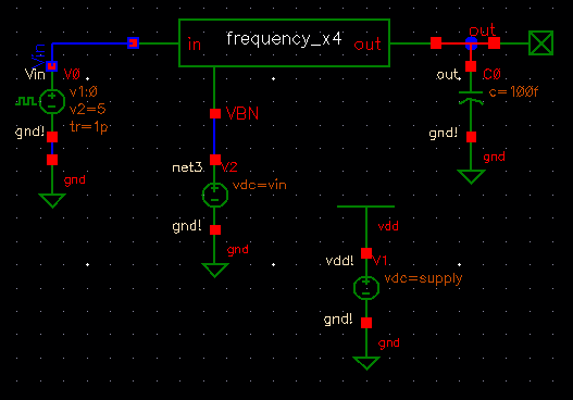
Figure 62, Simulating the Times Four
(x4) Clock Multiplier at 9MHz, with variable supply.
Launching the
Analog Design Environment, loading a previous state, and clicking Setup -> Environment:
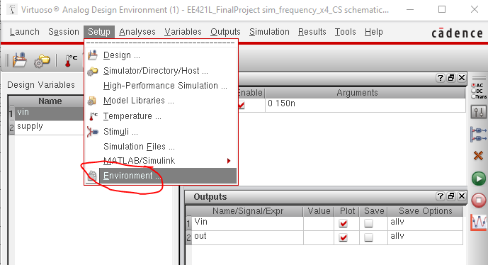
Figure 63, Menu of the ADE, Setting up
the Environment
In the
Environment Window, placing the word “extracted” in front of “schematic”:
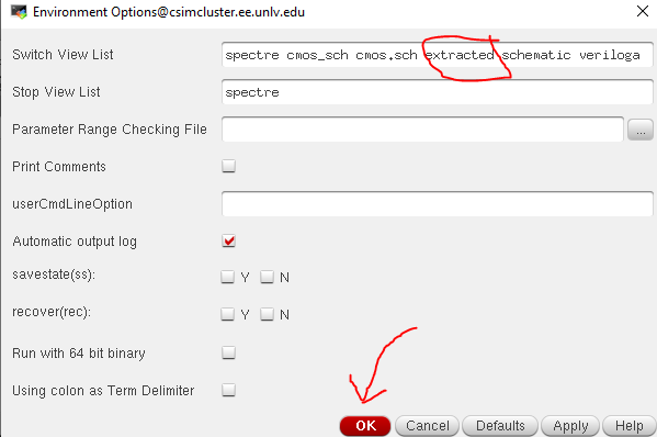
Figure 64, Setting up the Environment
to run the Extracted view of our Clock Multiplier
Setting vin
(VBN) to 1.15V, and doing a parametric analysis of the supply voltage:
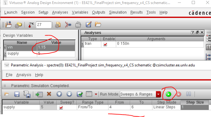
Figure 65, Setting up the Parametric
Analysis on our Extracted circuit:
Results:
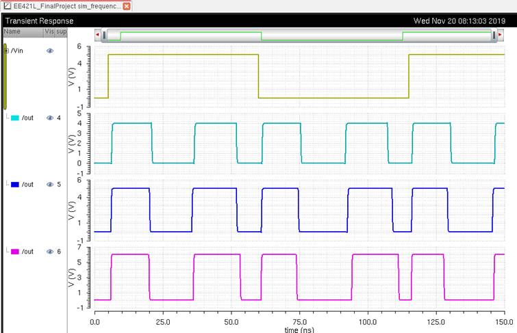
Figure 66, Simulation of the Extracted
Circuit, Input Frequency = 9 MHz, VBN =1.15V, Voltage Supply (4V Turquois, 5V Blue, 6V Magenta), Using Current Starved (CS) Inverters
Now to prove
that we have ran the extracted view, in the ADE, Simulation -> Netlist ->
Display:
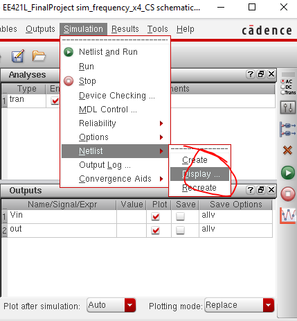
Figure 67, Steps to view if we ran the
Extracted View
Results:
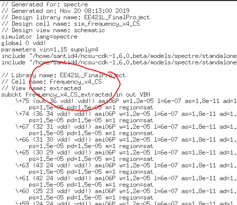
Figure 68, Proof that the Extracted
View Ran!
Now, we will download
the entirety of the project, “EE421L_FinalProject.zip” and you can view the files
here.
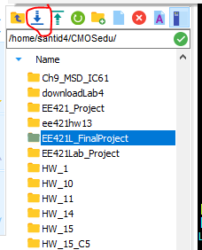
Figure 69, Nice.
Conclusions II:
For the lab
layout, we got to see the positives of creating many cell views, in which all
the rule checks and verifications worked out much easier and faster.
The only
negative with this approach is that layouts will not be optimized, and there
are some instances that could have merged into a compact form.
For the bodies
of the long length inverters, those have been changed so that the bodies of all
PMOS/NMOS devices are connected to VDD!/GND!,
respectively, so that the layout will be smaller and compact.
For this
class, the body effect can be considered negligible, however, it plays a role
when going into analog design.
This ends part
II of the final lab project, and of the report.
------------------------------------------------------------------------