Lab 7 – Using Buses and Arrays in the Design of Word Inverters, Muxes, and High-Speed Adders
EE 421L Digital IC Design
Lab Date: 10/23/19 Due: 11/06/19
Last Edited on
11/05/19 at 11:02am using Word
We will first
look through Tutorial 5 and learn how to create a Ring Oscillator using buses.
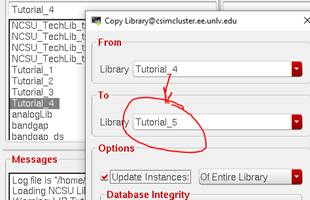
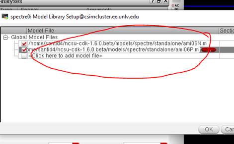
Copying
Tutorial_4 to a new library, Tutorial_5:
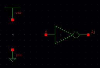
Creating a new
schematic cell, ring_osc, with one inverter:
Pressing bindkey c (copy), clicking on the Inverter, and then pressing F3:
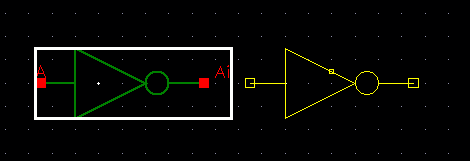 (Copying)
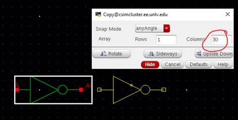 (Press F3, type 30, Click on exact area as
shown)
(Press F3, type 30, Click on exact area as
shown)
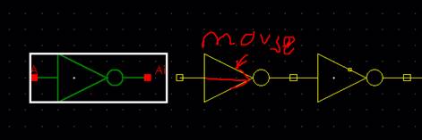 (Drag mouse to the right)
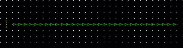
Repositioning
the first inverter to get the following:
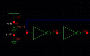
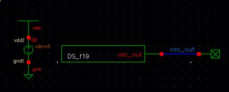
Placing labels
and the DC Voltage supply:
Now, setting
up the ADE L:

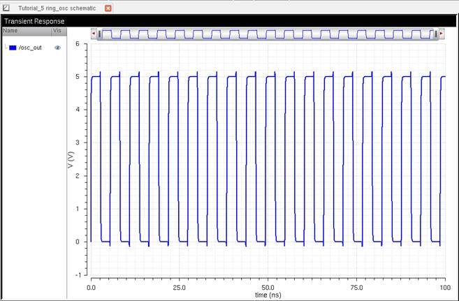
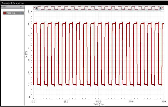
Results:
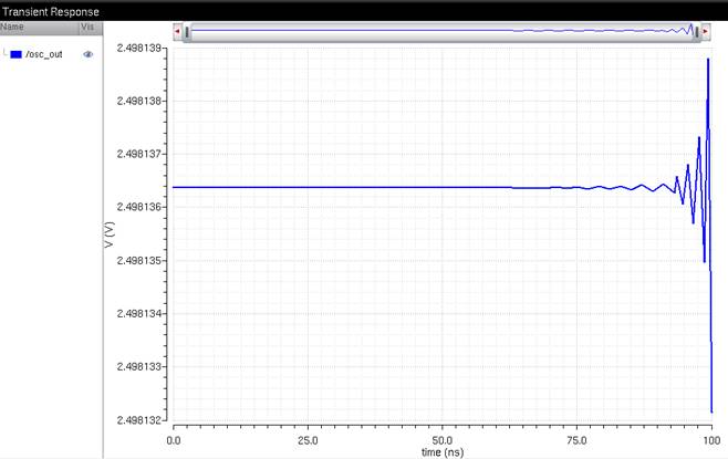
Noise will
kick start this circuit. If we want to get this circuit to work, we will set
the initial condition at the input of the first inverter to 0.
In the ADE,
Simulation -> Convergence Aids -> Initial Condition:
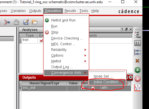
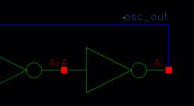
Set the Node
Voltage to 0, then click on the label “osc_out”
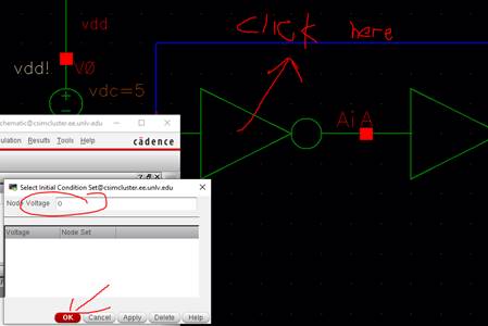
If you see the
following, then the initial condition is set.
Check and save, and rerun the simulation.
Close the ADE.
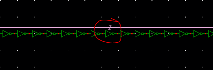
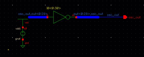
With the same
schematic, we will make this ring oscillator look neater.
Delete all of the inverters except the first inverter.
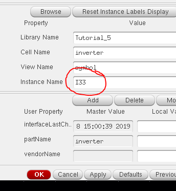
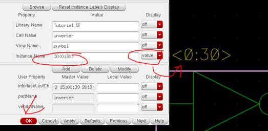
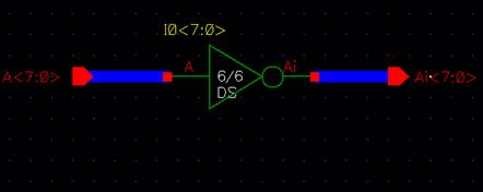
Change the name
of the inverter to I0<0:30> (or I0<1:31>).
Using bindkey Shift+W to create a wide
wire, place this bus wire on the input and output of the inverter.
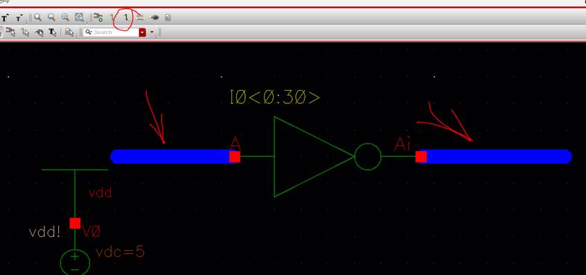
Use labels to
connect the bus wires together.
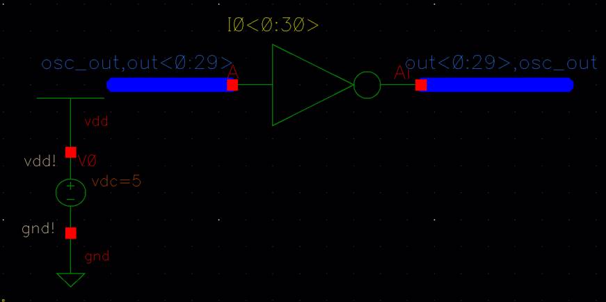
The first
label is the input of the first inverter I0<0>.
The 2nd-31st
input labels are the inputs to Inverters I0<1:30>
The 1st-30th
output labels are the outputs of Inverters I0<0:29>
The 31st
output label is the output of the 31st inverter I0<30>
Close all cell
views.
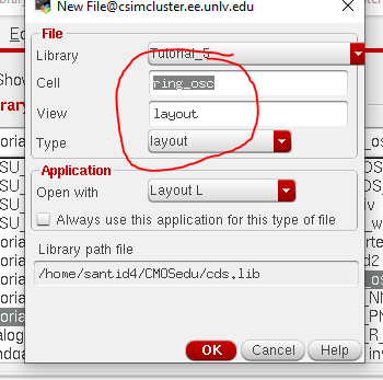
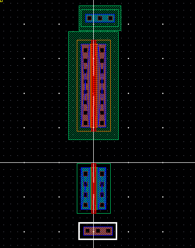
Now, creating
a layout for our ring oscillator:
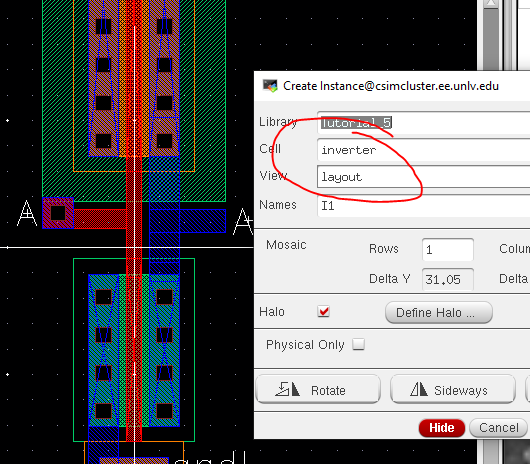
Instantiating
our inverter layout:
For this
special tutorial, we will do this from scratch and make our ring oscillator a
bit smaller.
Instantiating
a 6μm/600nm NMOS and 12μm/600nm PMOS, with ntaps
and ptaps:
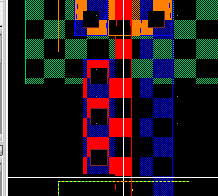
Connecting the
gates together with a poly rectangle, also connecting the right side metal1
layers:
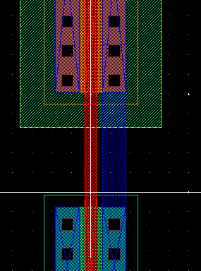
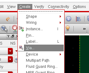
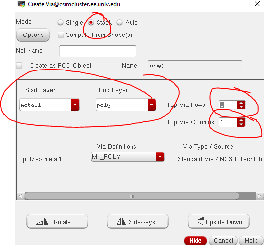
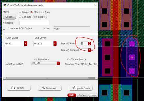
Going to
Create-> Via, and instantiating a m1 to poly contact:
Now copy and
paste this NMOS and PMOS once
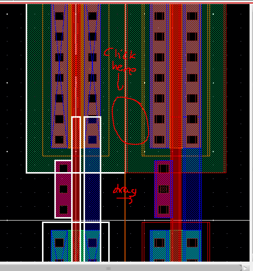
Now, lets wire
these inverters up as follows:
NOTE: Make sure to make the m1 wires
connecting from the MOSFET to vdd!/gnd! are a little longer. This
will save much headaches if you do need to make the inverter a bit “taller”.
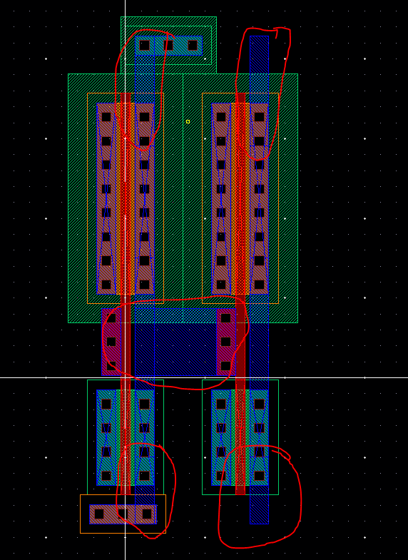
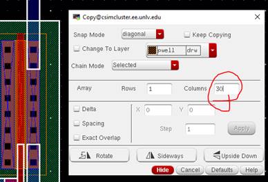
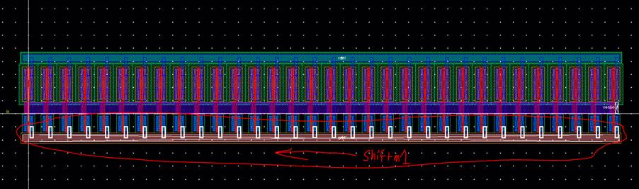
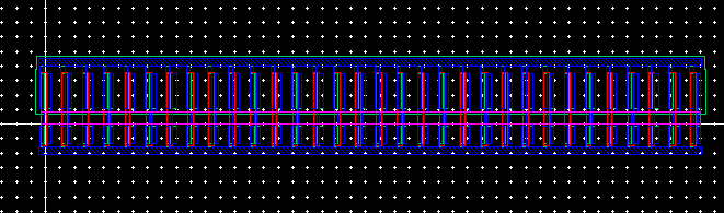
Copying and
pasting the 2nd inverter another 29 times using F3:
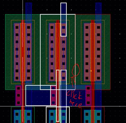
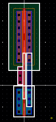
DRC:
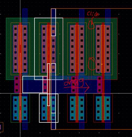
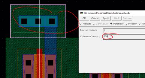
Clicking on
the ntap/ptap and pressing bindkey q, size up the number of columns to fit all of the inverters together. You may need to keep changing
the columns to fit your needs.
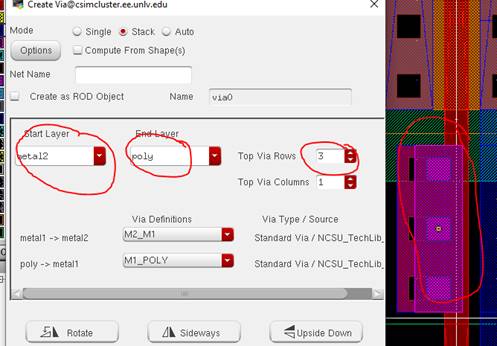
Recalling that
the output of the last inverter is the input of the first inverter, instantiate
a 3x1 (3 rows, 1 column) m1_m2 via at the output of the final inverter, and
then instantiate a 3x1 m2_poly via at the input of the first inverter.
Output of last
inverter:
Input of first
inverter:
Draw a metal2
rectangle from the output of the final inverter to the input of the first
inverter:
Creating pins
for vdd!,
gnd!, and osc_out all on m1
(Note, osc_out is an output, while the others are
input/outputs):
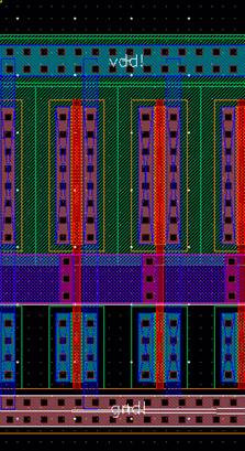
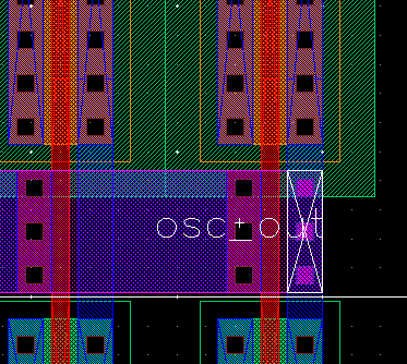
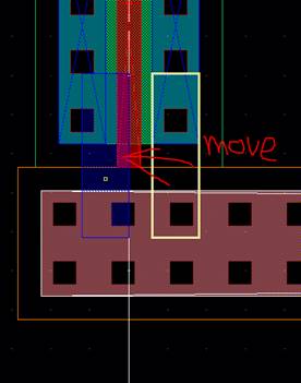
Realizing that
the NMOS and PMOS metal1 rectangle is on the wrong side (should be on the left)
and pressing bindkey m (move).
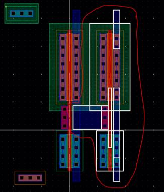
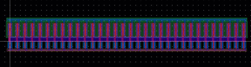
Final layout: 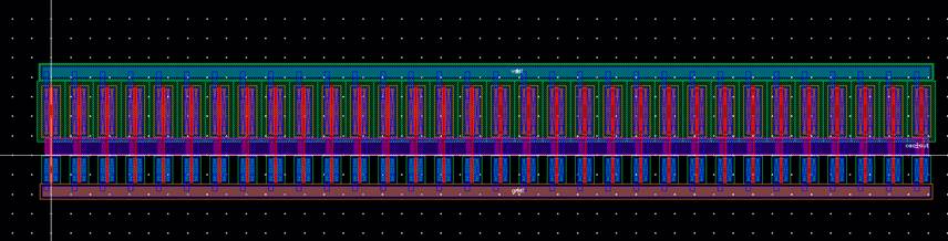
DRC:
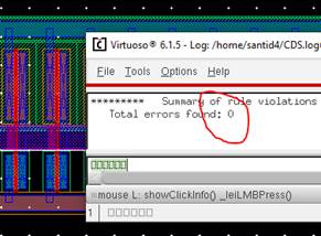
Save all.
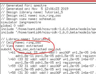
Extract:
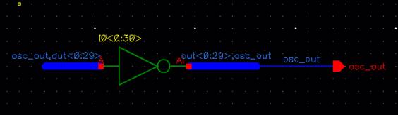
Recalling that
we need to have a pin, osc_out in our schematic:
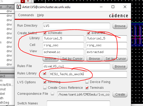
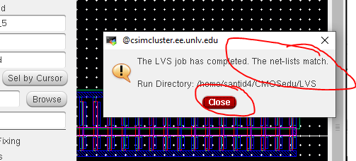
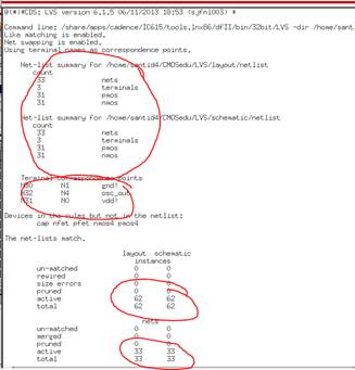
LVS:
Close all cell
views.
Creating a
symbol for our ring oscillator schematic:
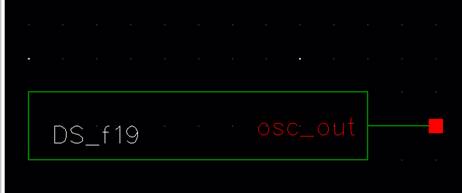
Creating a
schematic, sim_ring_osc:
We will resimulate the ring oscillator as we have done before.
Setting up the
initial condition of 0 at osc_out, and setting up the
ADE and plotting the output:
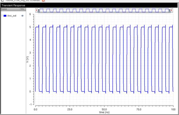
Now, lets
simulate the layout. Since the LVS passed (the extracted view’s nodes match the
schematic view’s nodes), we should get the same output.
Setting up the
ADE to simulate the extracted view (Setup -> Environment)
:
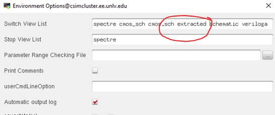
Checking that
it ran the extracted view (Simulation -> Netlist -> Display):
This concludes
the prelab.
--------------------------------------------------------
Experiment 1: Creating a 4-bit
word inverter, with simulation:
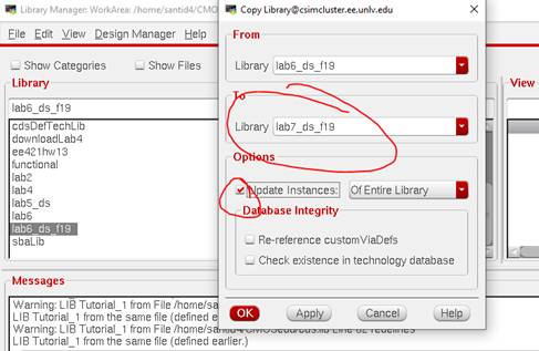
Copying lab6’s
library to a new library, lab7_ds_f19:
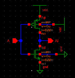
For this lab,
we will need 6u/600n PMOS/NMOS inverters.
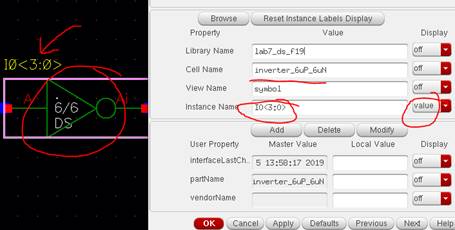
Creating a
cell, inverter_6uP_6uN:
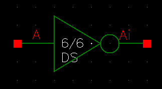
Symbol:
Creating a
cell, inverter_4_bit, with symbol:
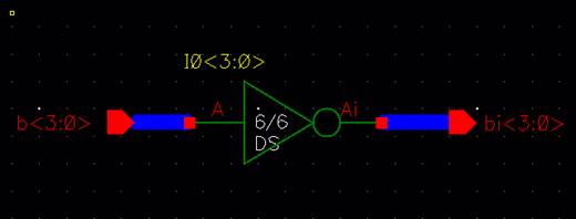
Symbol View:
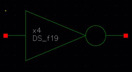
Creating a
schematic, sim_inverter_4_bit_DS_f19:
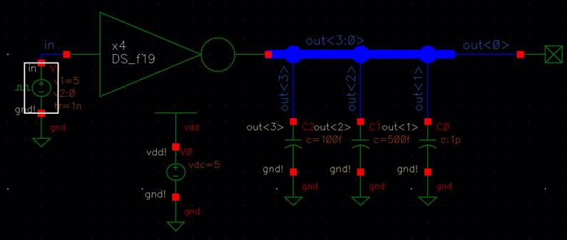
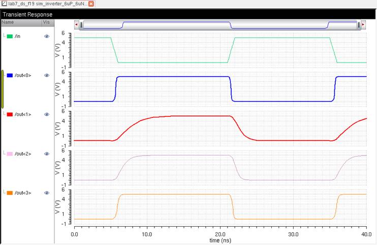
This makes
sense.
Out<0>
has no load, therefore, the rise and fall time are fast.
Out<1>
has the heaviest load (big capacitor relative to others), giving it a higher RC
time delay. Note that the tPLH is greater
since when the input is LOW, the PMOS is turned ON and has a higher effective
resistance than the NMOS, therefore, we have a larger Time Constant.
This same
analogy can be applied to the other loads.
-----------------------------------------------------------------------------------
Experiment 2: Schematics and
Symbols of: 8-Bit Input/Output array of NAND, NOR,
AND, Inverter, and OR gates
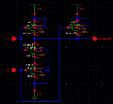
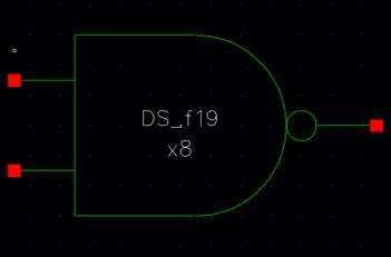
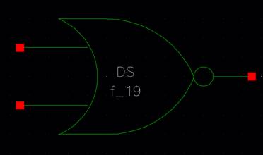
NAND Gate:
First,
creating a schematic cell, nand_8_bit_DS_f19, with corresponding symbol:
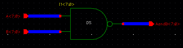
8-bit word
symbol:
Simulation:
For the next
few gates, we will be using a cell, sim_gate, to sim
8-bit words.
For A, A<7:0> = 1010 1010,
nand B<7:0> =
0011 0011.
C<7:0> =
A nand B = 1101 1101
Results:
This is the
8-bit bitwise NAND gate.
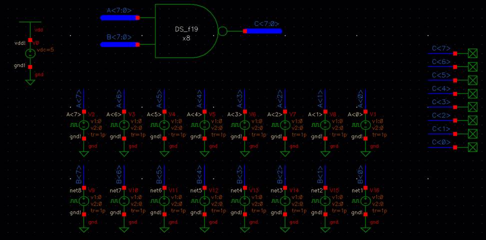
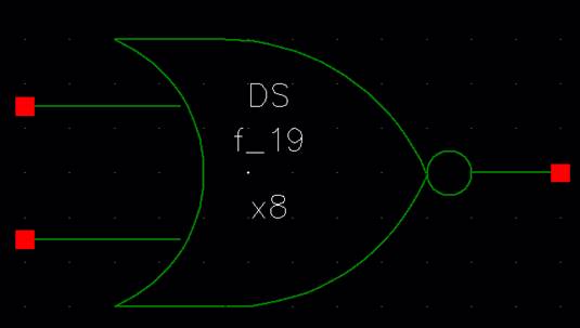
NOR Gate:
Schematic of NOR gate:
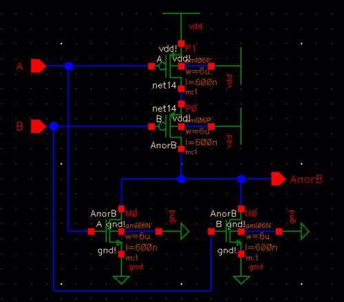
2 input symbol:
8-bit word
schematic:
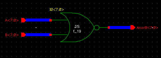
8-bit word
symbol:
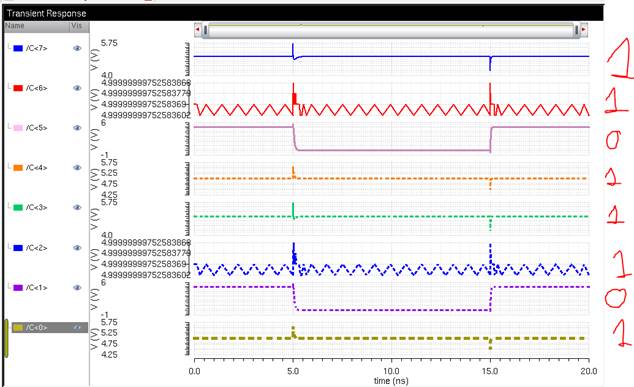
Simulation:
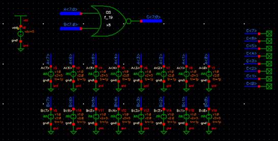
Using our same
numbers:
For A, A<7:0> = 1010 1010,
nor B<7:0> = 0011 0011.
C<7:0> =
A nor B = 0100 0100
Result:
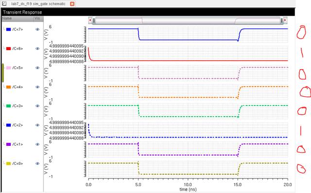
Perfect. This
is the 8-bit bitwise NOR gate.
AND Gate:
This one is
simple. We will just take the NAND gate and throw it through an inverter to
make it an AND gate.
By analogy:
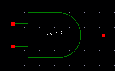
Schematic of
AND gate:
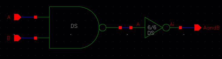
2 input symbol:
8-bit word
schematic:
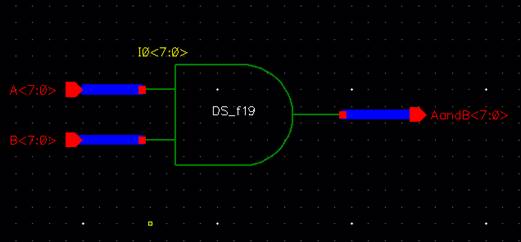
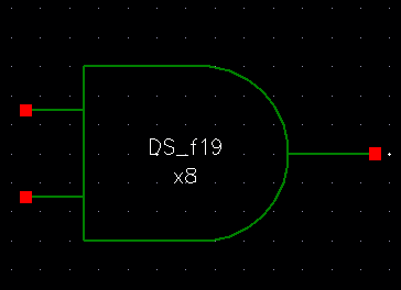
8-bit word
symbol:
Simulation:
Using the same
words as used with the NAND gate, we will get the output results of the NAND
gate, but inverted.
For A, A<7:0> = 1010 1010,
AND B<7:0> = 0011 0011.
C<7:0> =
A and B = 0010 0010
Results:
Sweet. This is
the 8-bit bitwise AND gate.
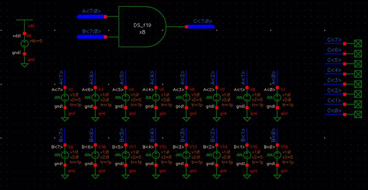
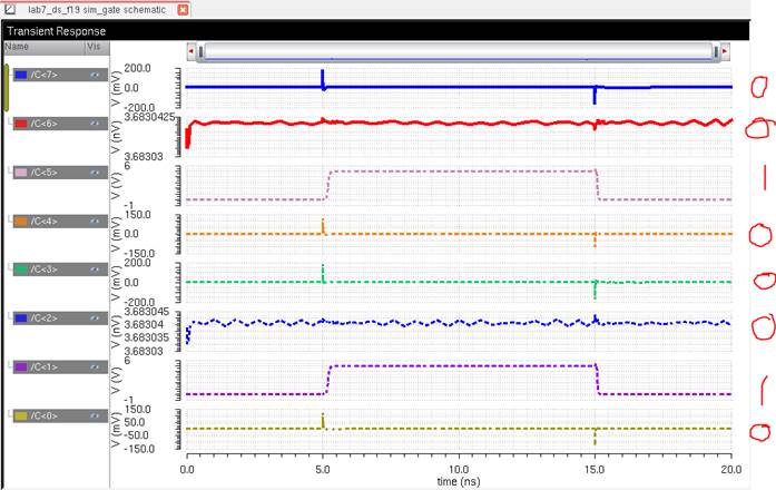
Inverter:
Just as similar to the first part of this lab, and since we have already
created a 6u/6u PMOS/NMOS inverter, by analogy:
8-bit word
schematic:
8-bit word
symbol:
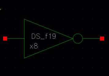
Simulation:
For this, we
will just take the input word A and invert it.
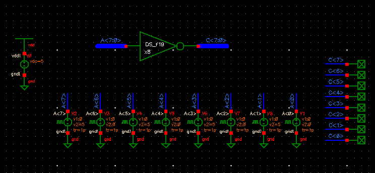
For our input:
A<7:0> =
1010 1010,
C<7:0> =
0101 0101,
Result:
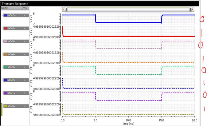
This is an 8-bit
word inverter.
-----------------------------------------------------------------------
Experiment 3: 2-to-1 DEMUX/MUX
First, lets do
the 2:1 MUX:
Creating a
schematic, MUX_2_1_ds_f19:
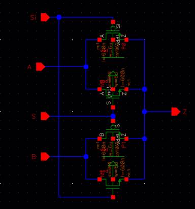
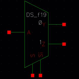
Symbol:
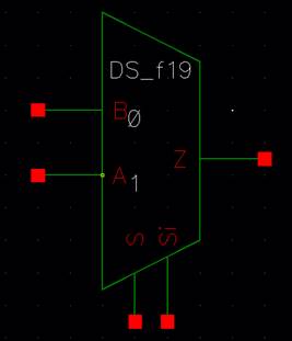
NOTE: We
placed 0 and 1 on the MUX to show the user what to do with the select S input.
Simulation:
Result:
For this MUX,
if we send a 1 to S, then it selects the input A to be outputted into Z. Else,
input B will be outputted to Z.
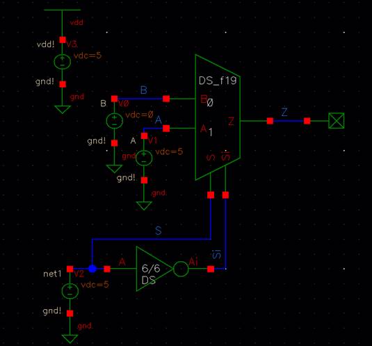
Now, lets do a
1:2 DEMUX:
Creating a
schematic, DEMUX_2_1_ds_f19:
Symbol:
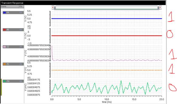
Simulation:
In this sim,
if we send a 1 to the select S, then we will grab the output line Z.
Else, we will
grab the output line Y.
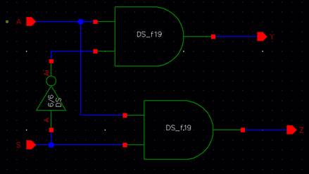
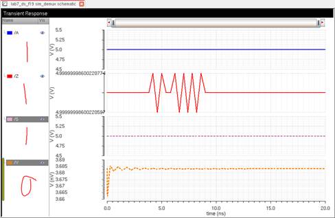
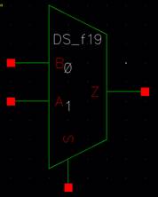
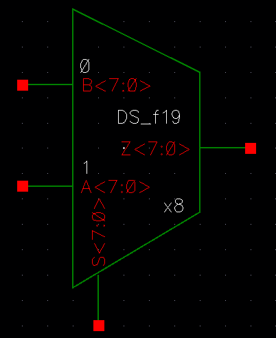
8-bit Word – 2:1 MUX:
Redesigning the 2:1 2-input MUX:
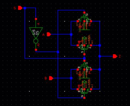
Schematic:
8-Bit Word Schematic:
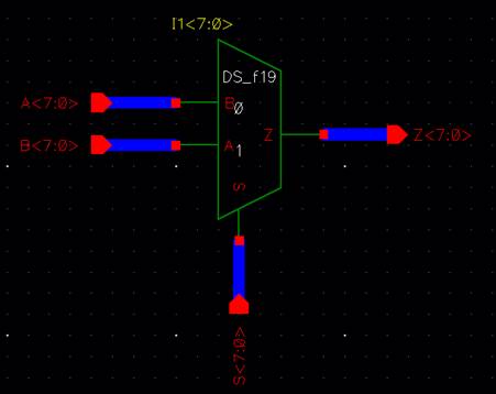
8-Bit Word
Symbol:
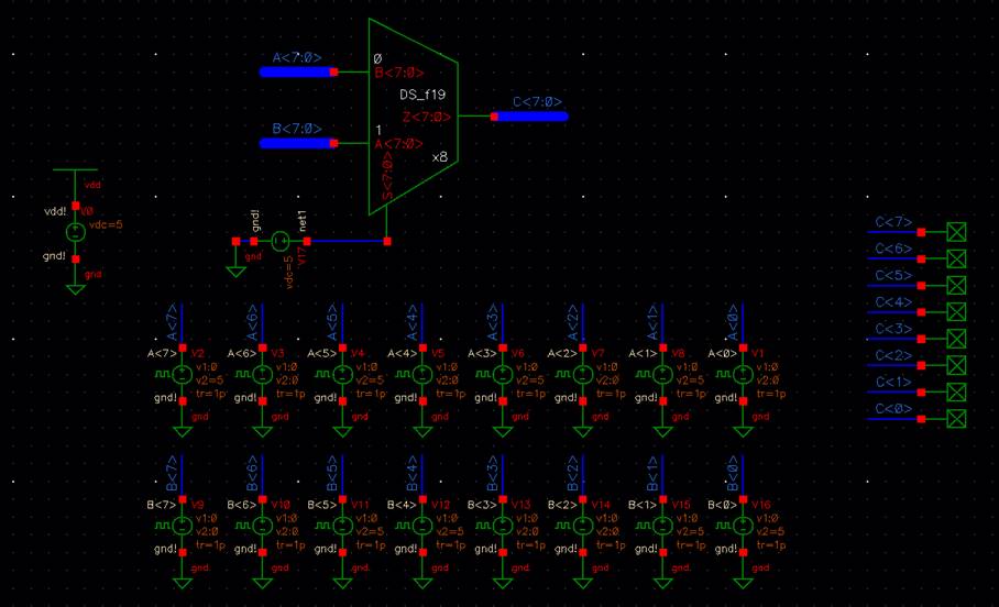
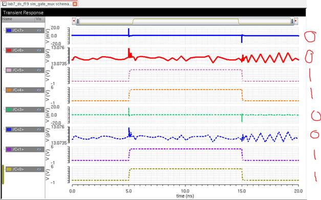
Simulations:
Using our
schematic cell, sim_gate, to choose a word to pass to
Z<7:0>:
Our select is HIGH, therefore, word B will pass. B<7:0> = 0011 0011
Results:
---------------------------------------------------------
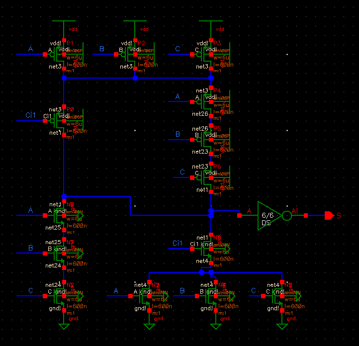
Experiment 4: The Full-Adder
Part 2:
We will have
the following schematic:
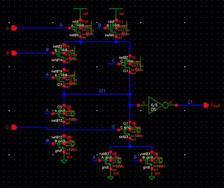
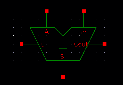
Symbol:
8-Bit Word
Adder Schematic:
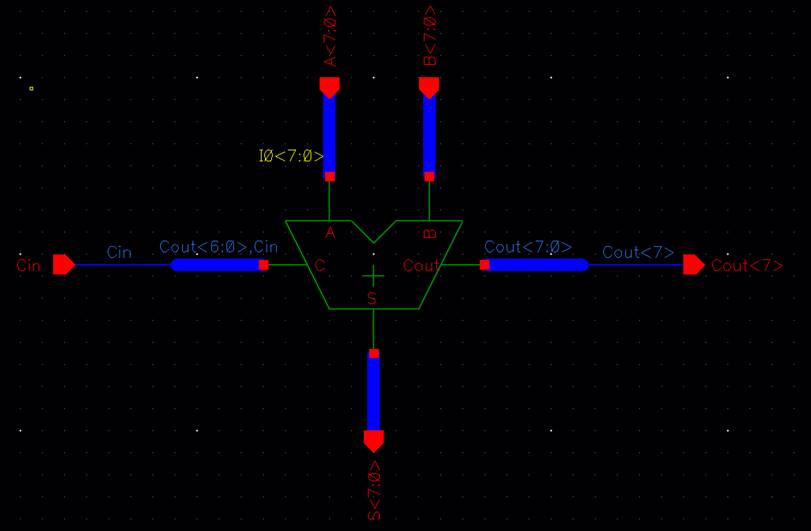
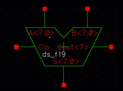
8-Bit Word
Symbol:
Simulation:
Using our
schematic, sim_gate, and the same words we used for
the bitwise operations:
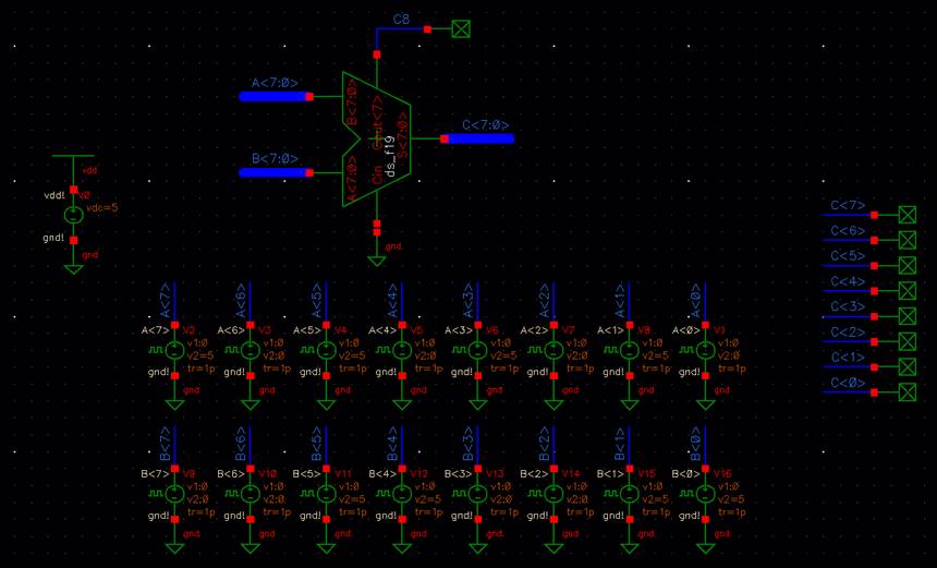
For A, A<7:0> = 1010 1010,
+ B<7:0> = 0011 0011.
C<7:0> =
A + B = 0 1101 1101
Results:
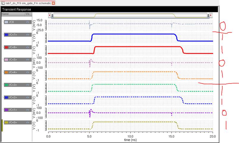
We have successfully
made our Full Adder.
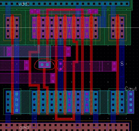
Layout of the Full Adder:
Laying out the
1-bit Full Adder:
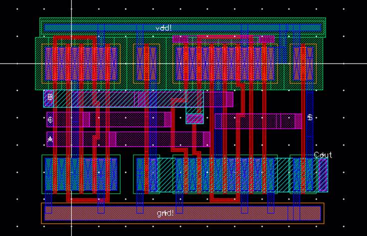
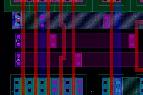
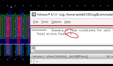
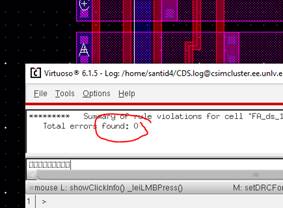
DRC:
Extracted:
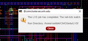
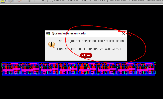
LVS:
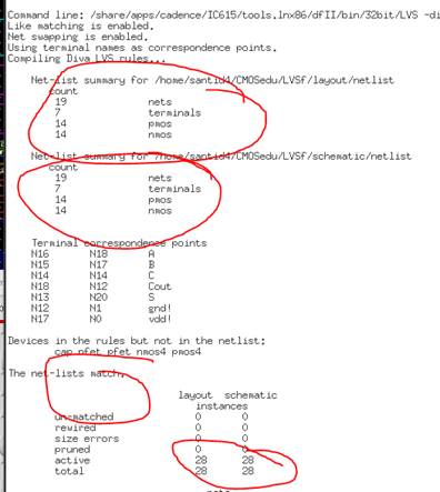
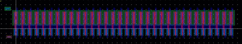
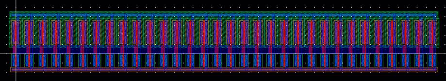
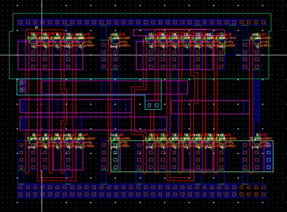
Laying out the 8-Bit Full
Adder:
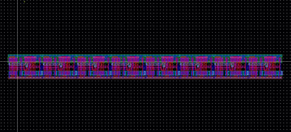
NOTE: Do NOT label
Cout<n> in between any of the Full Adders. Only
Cout<7> should be labeled in the layout.
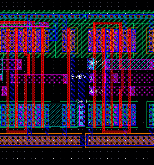
Note Cout is labeled, but is not really
there. It was carried over from instantiating the single full adder.
This Concludes
Lab 7.