Lab 6 – Design, Layout, and Simulation of a CMOS NAND Gate, XOR Gate,
and Full-Adder.
EE 421L Digital IC Design
Lab Date: 10/09/19 Due: 10/23/19
Last Edited on
10/21/19 at 6:36pm using Word
Before we
start the lab, we will need to look at Cadence Tutorial 4 on CMOSedu.com
Table of
Contents:
Experiment 1: Layout of the NAND Gate, with Simulation
Experiment 2: Layout of the XOR Gate, with Simulation
Experiment 3: Layout of the Full Adder, with Simulation
Prelab:
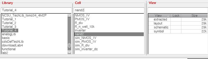
First, copy
Tutorial_3 to a new library Tutorial_4 in the Library Manager.
Then copy the
inverter cell to a new cell, “nand2”.
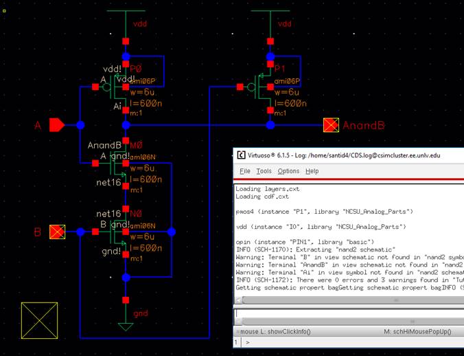
Create the
following schematic in nand2.
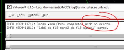
Check and save
to receive the following warning:
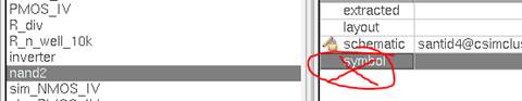
Delete the
copied nand2 symbol:
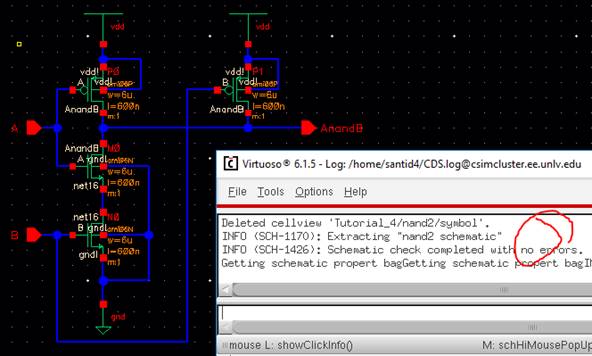
Check and
save.
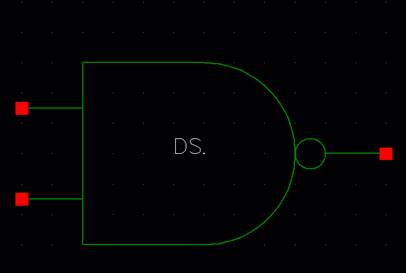
Create the
following symbol for nand2:
After Checking
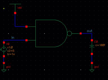
and Saving, Create a new schematic, sim_nand2_tran,
and draft the following:
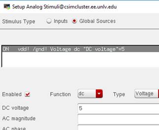
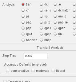
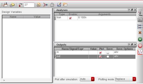
Launching the
ADE, and setting up the simulator (and saving the state):
Output:
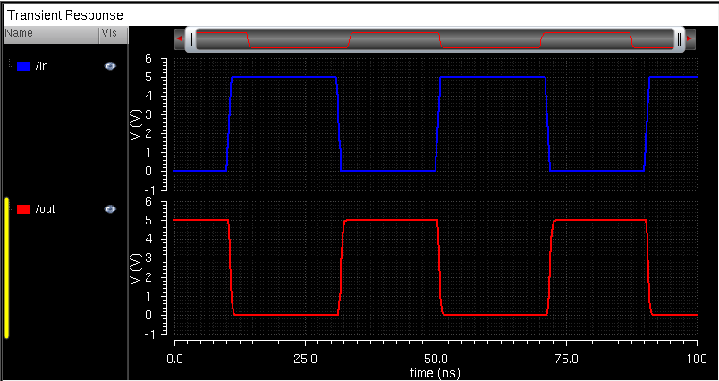
The NAND gate
behaves the way we want it to. Input A is 5V, and anytime Input B is 5V, the
output is 0V. Else, 5V.
Close and save
everything.
Creating
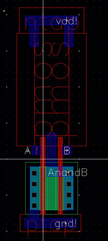
Layout:
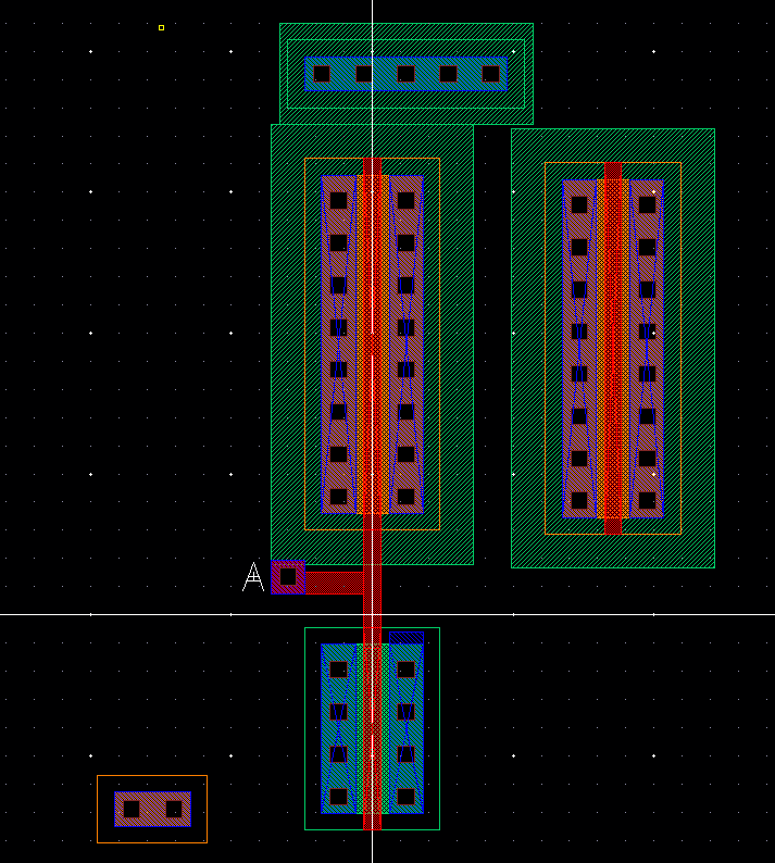
Copy/Paste
stuff:
Combine by
dragging:

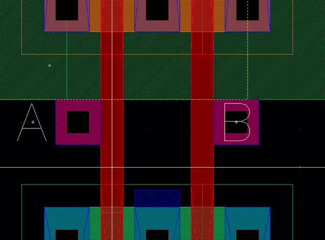
Create Pins:
Flattening out
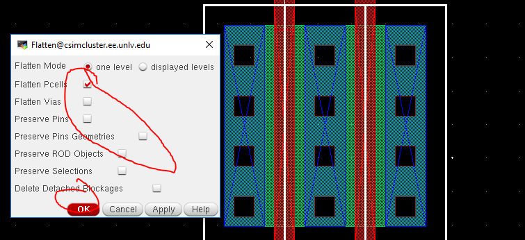
the bottom NMOS (Edit -> Hierarchy -> Flatten):
Delete the
metal1 and contacts in the NMOS:
Last, create
pins:
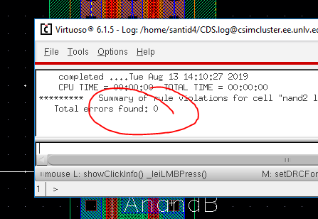
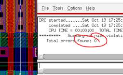
DRC the
layout:
Extract the
layout:
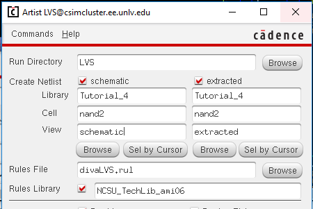
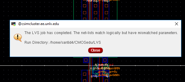
Running the
LVS:
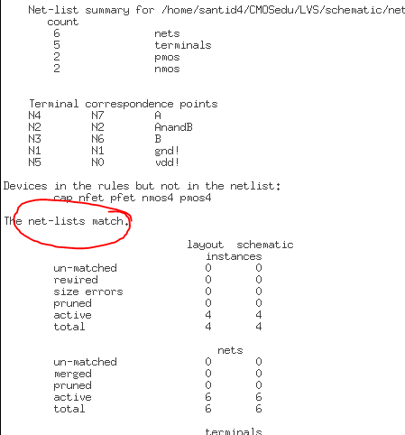
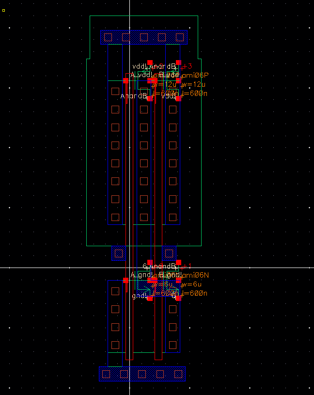
NOTE: The size of the PMOS in the extracted layout
shows “W=12u, L=600n”, whereas the PMOS in the schematic is “W=6u, L=600n”
Knowing that
the PMOS in the schematic doesn’t match what we have in the layout, change the
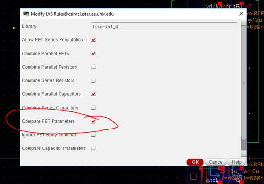
LVS rules by closing the LVS, and in the Extracted window, NCSU -> Change
LVS Rules:
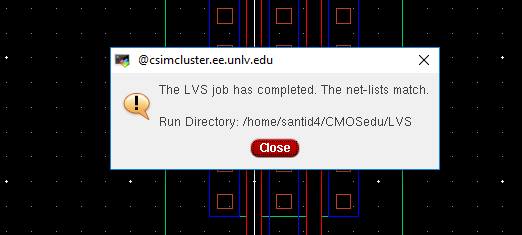
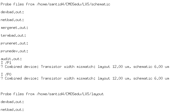
Rerunning the
LVS gives us the following error:
This ends
Tutorial 4 and the Prelab.
--------------------------------------------------------------------
Experiment
1: Creating the 2-Input NAND Gate, with Simulations
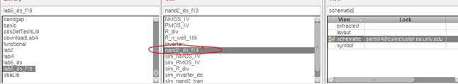
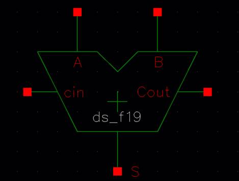
Creating a
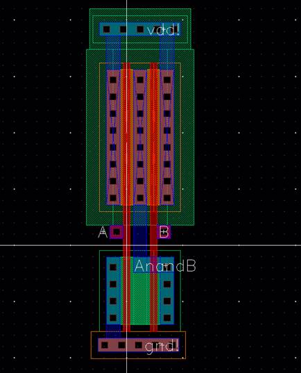
cell, “nand2_ds_f19”:
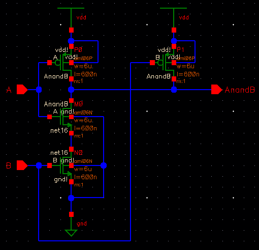
2-Input NAND
Gate Schematic:
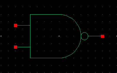
Symbol:
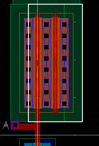
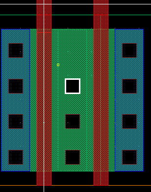
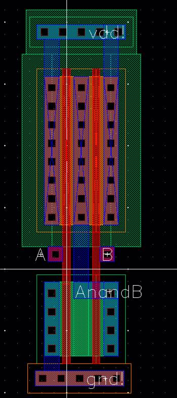
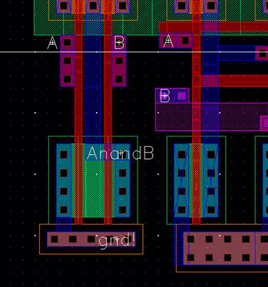
Layout:
DRC:
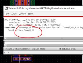
Extracted:
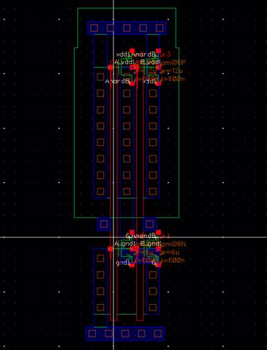
NOTE: PMOS sizes from layout and schematic are
different.
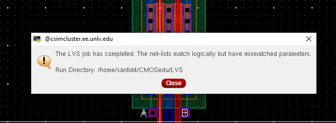
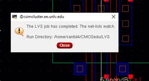
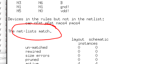
LVS:
TO FIX:
We notice that
using a ruler on the PMOS, we get a W = 12μm!!! This was due to
copy-pasting the Inverter layout.
We will just
change the size of the PMOS to a W=6μm.
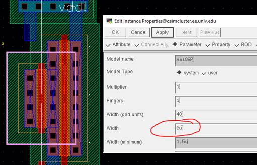
Resizing and
moving a few layers of the layout:
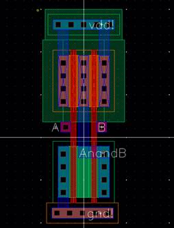
DRC:
Extracted:
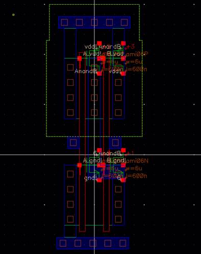
LVS (2nd
time with FET sizing):
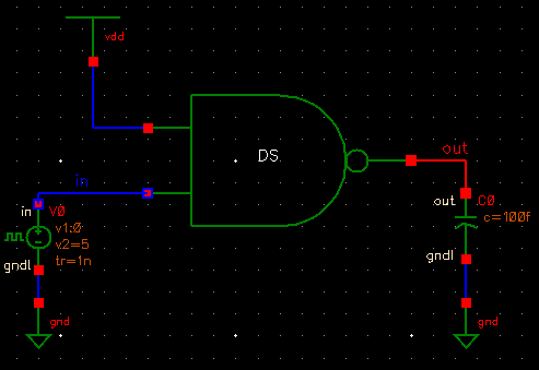
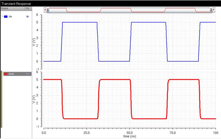
Simulation 1: Testing the NAND
Gate
This first simulation
is basically showing that when one input is HIGH, that the output will be
logical LOW when Vin is HIGH and logical HIGH when Vin is LOW (properties of
NAND Gate). This is basically an Inverter, and can be
useful if you need an oscillator with an ENABLE feature.
Simulation 2: Truth Table of
the NAND Gate
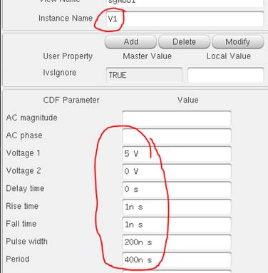
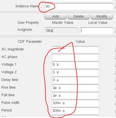
Now, lets
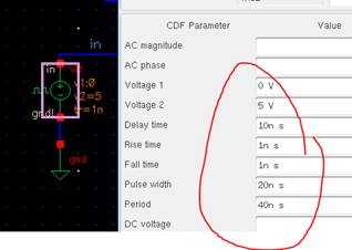
create a simple truth table by using pulse sources at the input of the NAND
Gate.
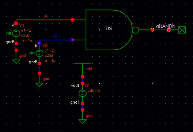
Input A: Input
B:
Results:
NAND Truth
Table
|
A |
B |
A NAND B |
|
0 |
0 |
1 |
|
0 |
1 |
1 |
|
1 |
0 |
1 |
|
1 |
1 |
0 |
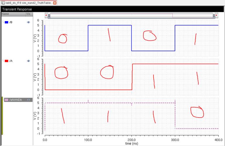
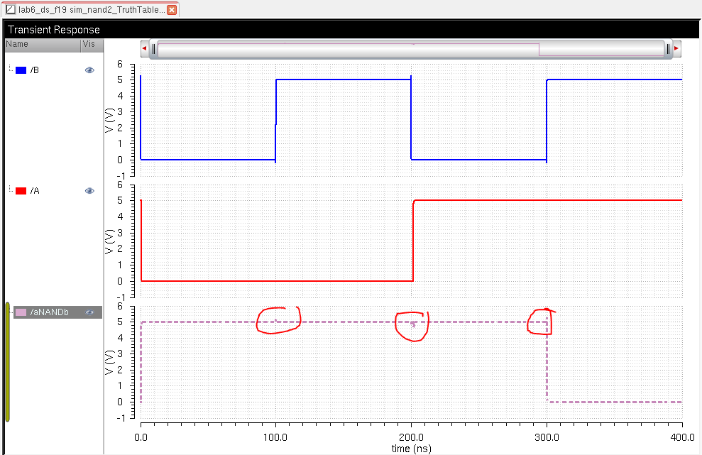
We see that
there are “glitches” in our output.
To remove them,
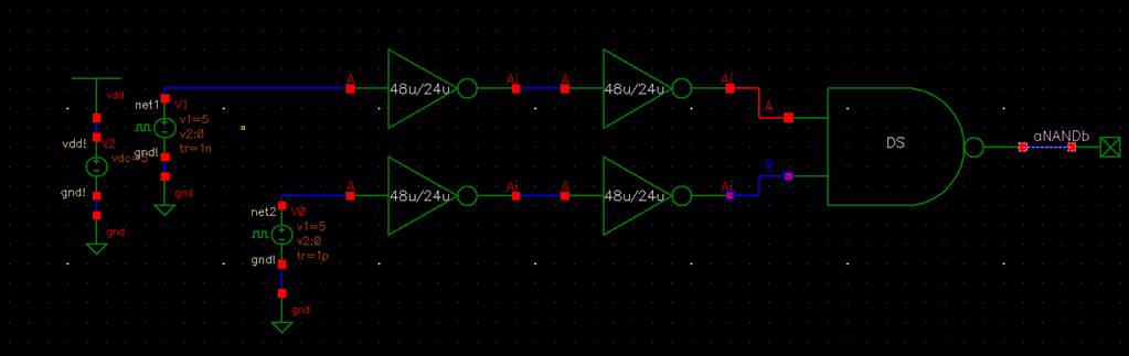
lets at a preamp double inverter stage using the inverters created in Lab 5:
From here, the
output looks much better, and the little “blips” are minimized.
------------------------------------------------------------------------------------------------------
Experiment
2: Creating the 2-Input XOR Gate, with simulations
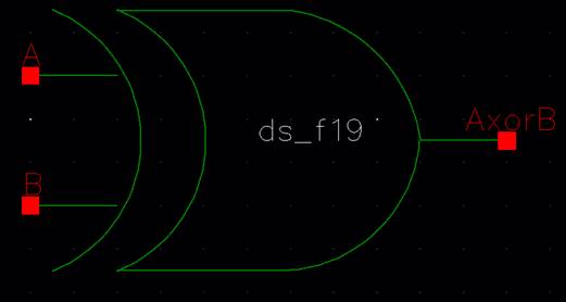
Creating a
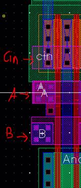
cell, “xor2_ds_f19”, with schematic:
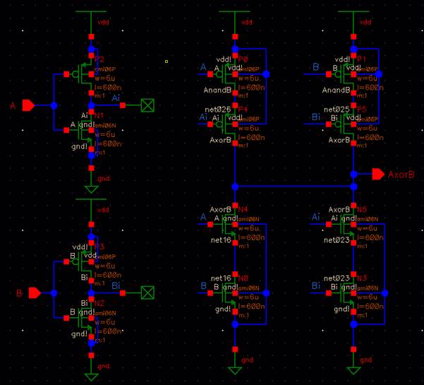
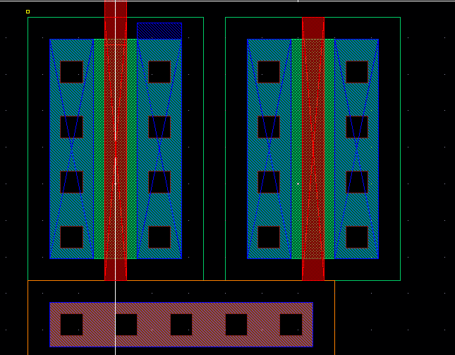
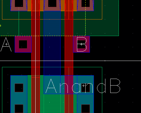
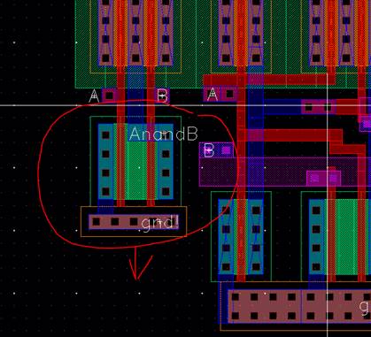
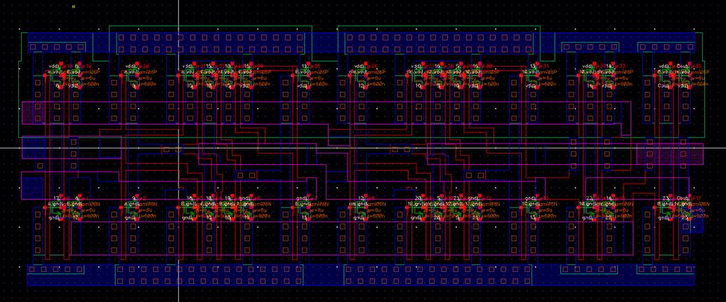
Layout of the
XOR Gate:
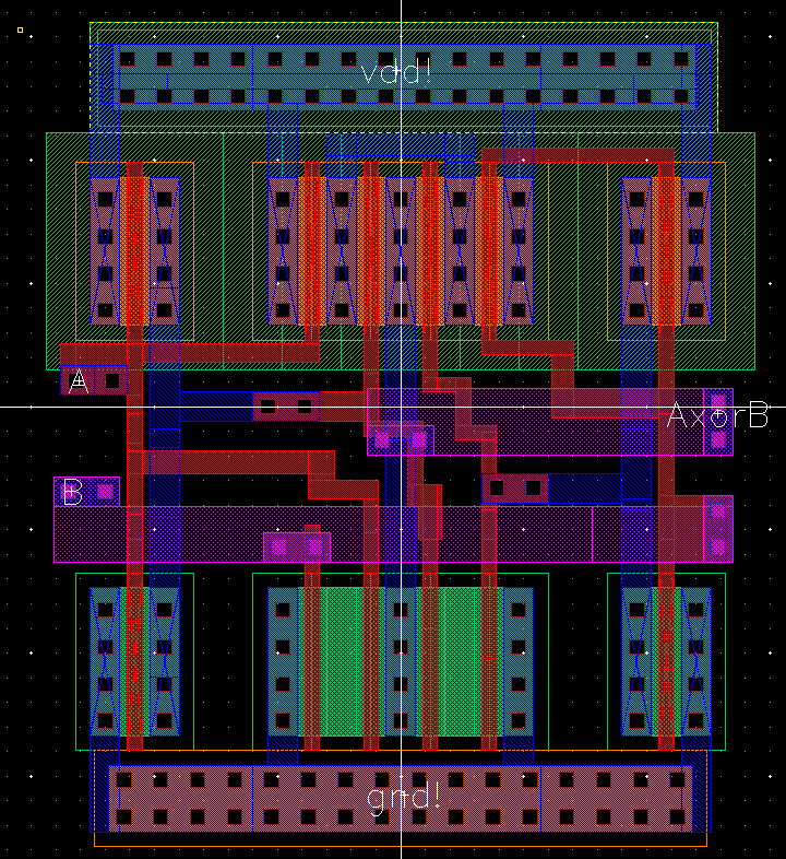
DRC:
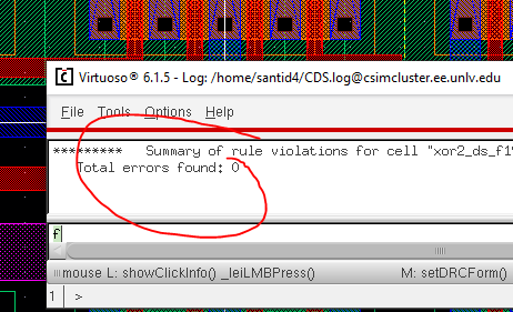
Extracted
View:
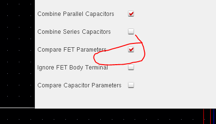
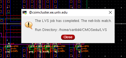
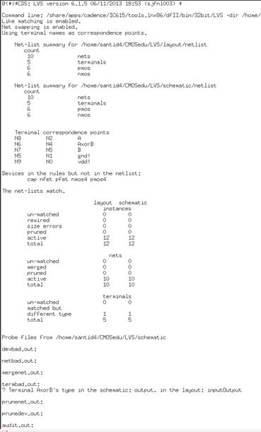
LVS:
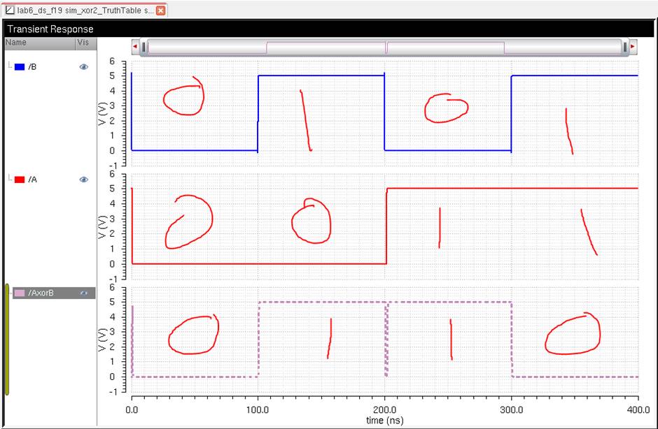
Simulation: Truth Table of XOR Gate
We will have
the following:
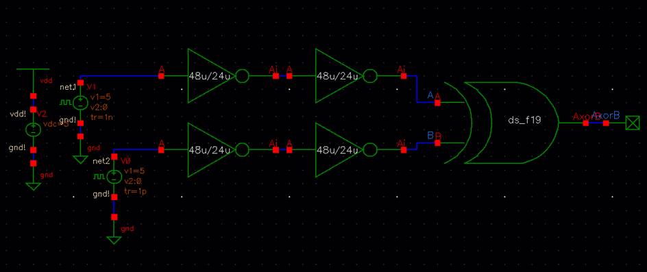
Output:
XOR Truth
Table
|
A |
B |
A XOR B |
|
0 |
0 |
0 |
|
0 |
1 |
1 |
|
1 |
0 |
1 |
|
1 |
1 |
0 |
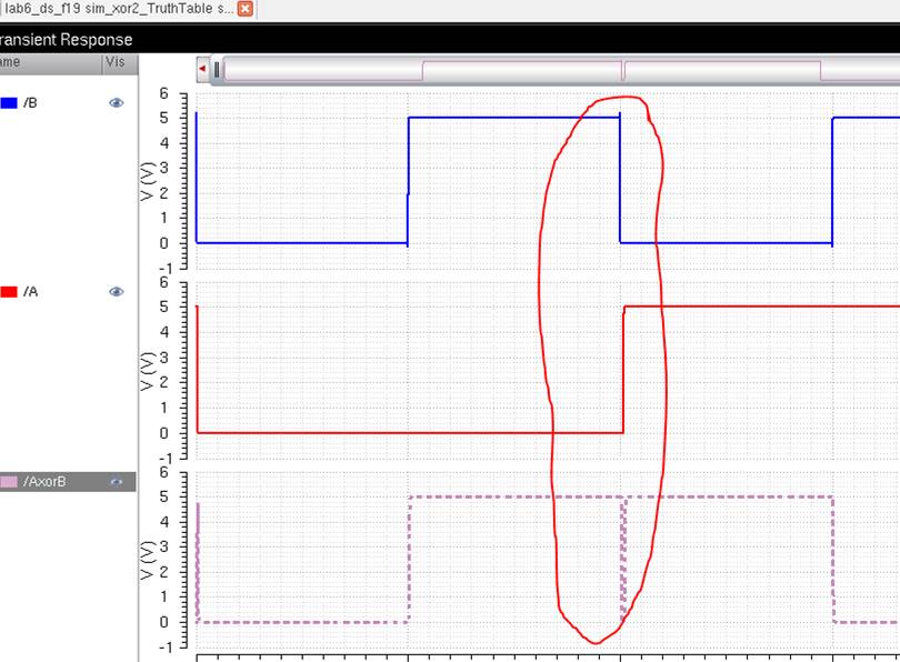
In this
specific gate, we do see that there is some sort of glitch that happens when
both A and B are transitioning at the same time.
Logically, if
A and B are the same input, therefore the output will be 0.
When both A
and B are switching as seen below, there is a moment where they are both equal,
therefore, the output will be 0 for a very small fraction of time. The
inverters will help give a quick rise time, but still will not be enough to fix
this glitch. Practically, this will always be there.
---------------------------------------------------------------------------------------------------------
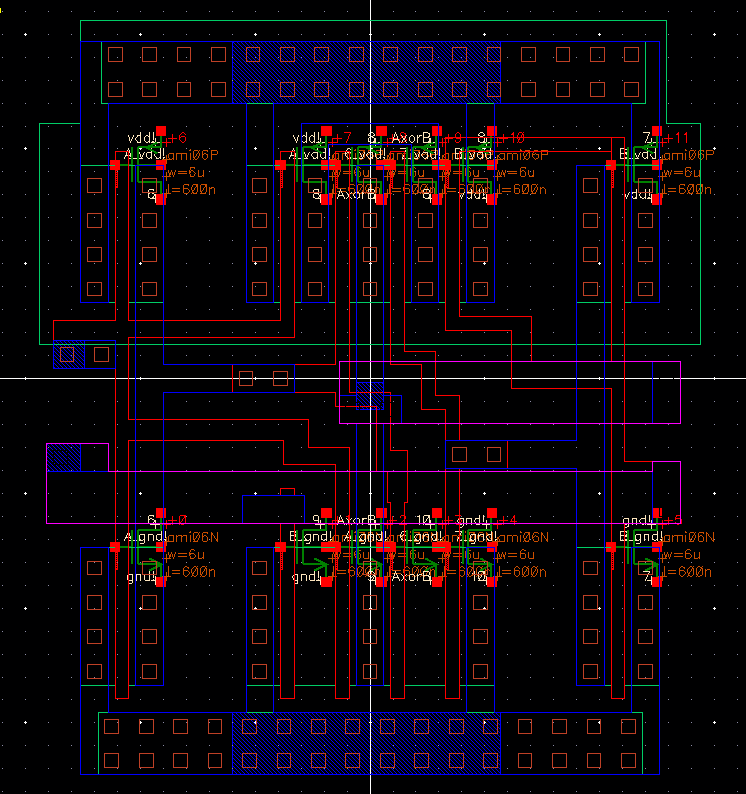
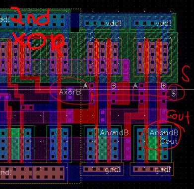
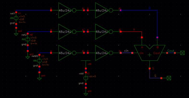
Creating a new
schematic using the NAND and XOR gates:
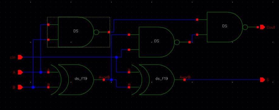
Changing the
height of the NAND Gate for compatibility:
Inputs: Outputs:
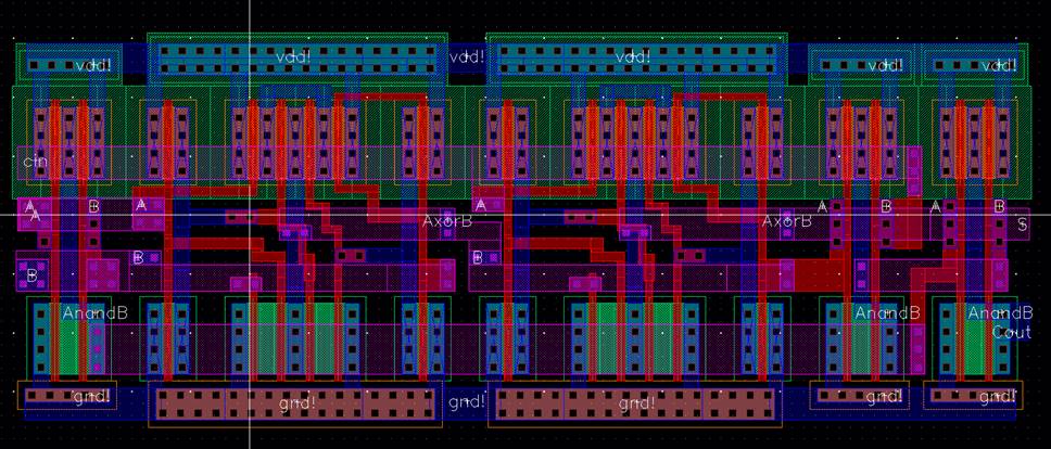
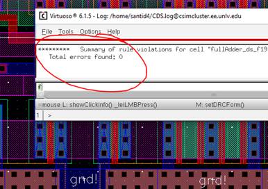
DRC:
Extracted:
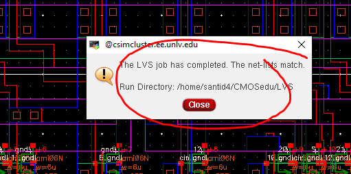
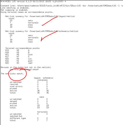
LVS:
Simulation: Truth Table of XOR Gate
Suppose we
have the following:
Results:
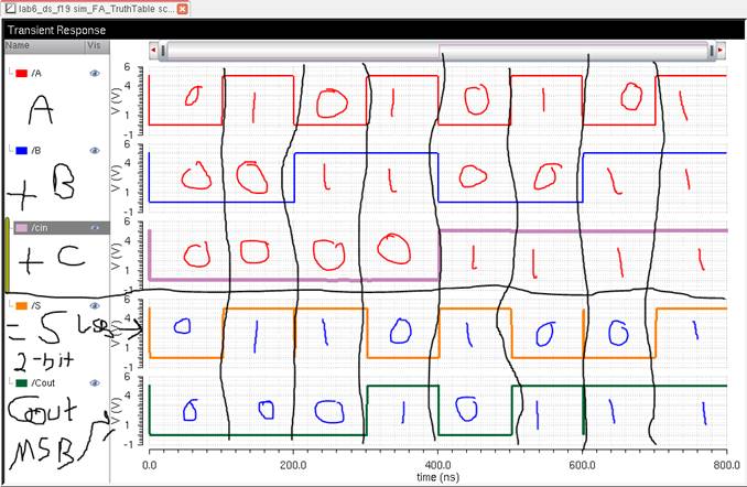
Full Adder
Truth Table:
|
Cin |
+ B |
+ A |
|
= Cout |
S |
Addition in Decimal |
|
0 |
0 |
0 |
|
0 |
0 |
0+0+0=0 |
|
0 |
0 |
1 |
|
0 |
1 |
0+0+1=1 |
|
0 |
1 |
0 |
|
0 |
1 |
0+1+0=1 |
|
0 |
1 |
1 |
|
1 |
0 |
0+1+1=2 |
|
1 |
0 |
0 |
|
0 |
1 |
1+0+0=1 |
|
1 |
0 |
1 |
|
1 |
0 |
1+0+1=1 |
|
1 |
1 |
0 |
|
1 |
0 |
1+1+0=2 |
|
1 |
1 |
1 |
|
1 |
1 |
1+1+1=3 |
Even though
there are those glitches in the simulation, the inverters help
out with trying to make the rise time of the inputs (rise time = fall
time = 1ns) much faster. We will always
have these kinds of errors in our practical circuits, but using an inverter is
a great way of minimizing the error at our output.
This Ends Lab
6
--------------------------------------------------------