Lab 5 – Design, layout, and Simulation of a CMOS Inverter
EE 421L Digital IC Design
Lab Date: 9/25/19 Due: 10/10/19
Last Edited on
9/26/19 at 11:52am using Word
Note: The files used for this lab can be
downloaded here.
Before we can
do this lab, we will first need to look at Cadence Tutorial 3.
Prelab:
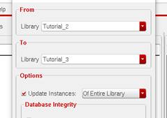
Assuming
Tutorial 2 has been completed, copy/paste it and create a new Library called
Tutorial 3.
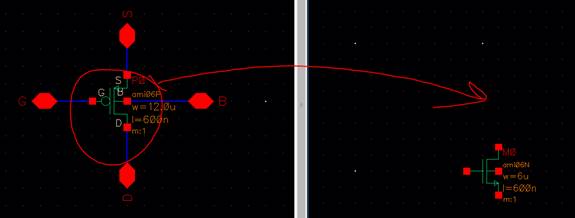
Creating a new
schematic, “inverter”, and opening up NMOS_IV schematic, we will copy/paste the
nmos4 instance to our new schematic by pressing bindkey
c.
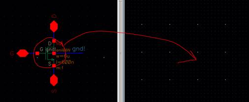
Close NMOS_IV,
and open PMOS_IV and do the same with pmos4.
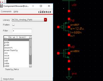
Instantiating
VDD and GND to our schematic (Bindkey I -> NCSU_Analog_Parts -> Supply_Nets):
Wire the
inverter, and add input pin A and output pin Ai:
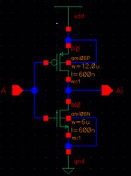
Check and save
the schematic.
Creating symbol
for this inverter to use in another schematic (Create -> Cell View ->
From Cell View):
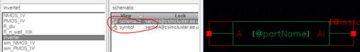
Create the
following:
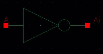
Check and Save
the symbol.
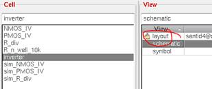
Create a new
layout window for the Inverter schematic.
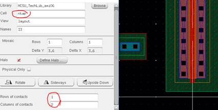
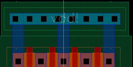
Add a
6μ/.6μ NMOS, 12μ/.6μ PMOS, ntap
(2 columns), ptap (2 columns), and m1_poly to the layout.
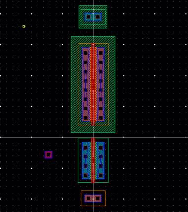
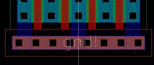
Organize the
layout (and running DRC):
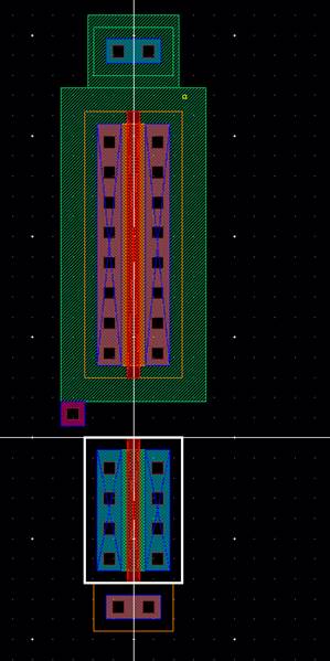
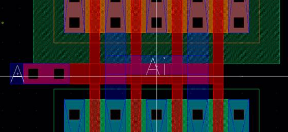
Add poly and
m1 rectangles to connect everything (Notice pin “A” is overlapping the PMOS, it
is okay since these 2 layers do not interact on same level).

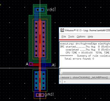
DRC the
connections:
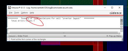
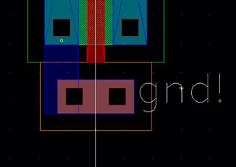
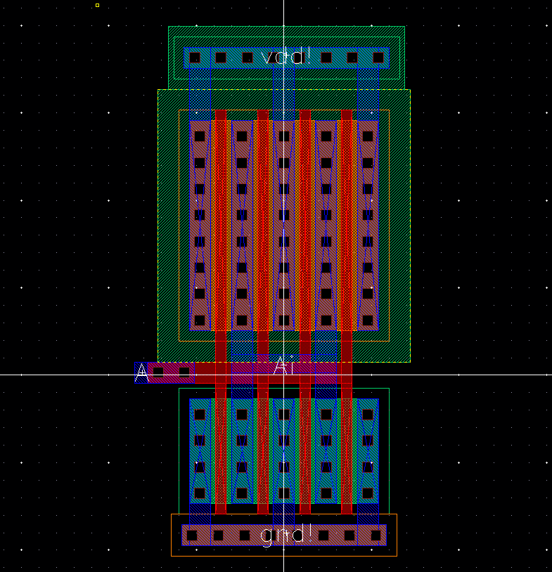
Add some blue rectangle
metal1 pins, where A is an input, Ai is an output.
DRC the
layout.

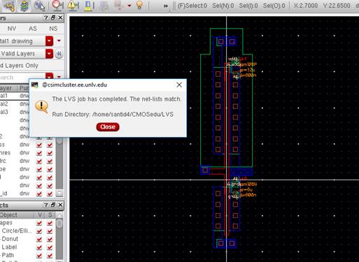
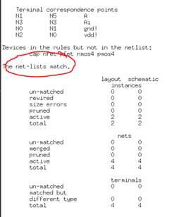
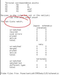
Extract the
layout, and LVS the extracted layout:
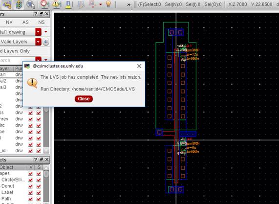
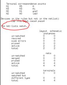
It passes the
LVS.
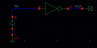
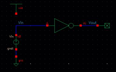
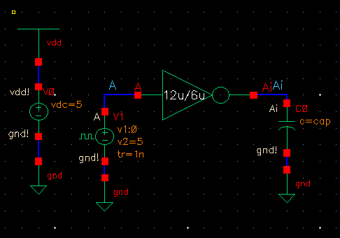
Make a new
schematic, “sim_inverter_dc”, and create the
following schematic:
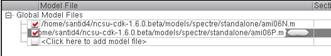
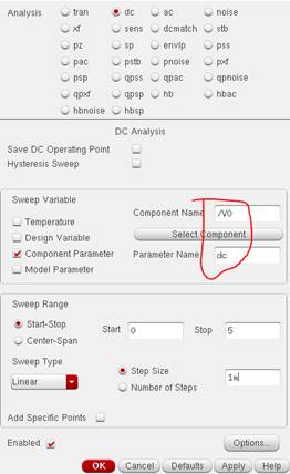
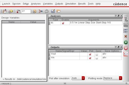
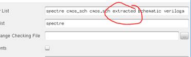
Launching the
ADE, and setting up the MOSFET models:
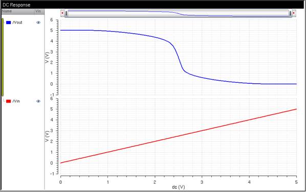
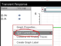
Results: (Using Graph -> Split Current Strip to see the 2
signals in 2 different graphs)
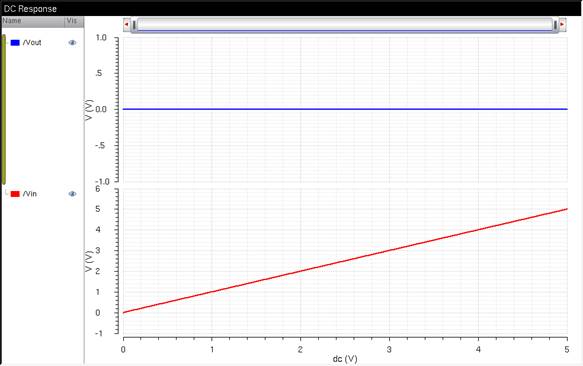
The Inverter with no Power
supply “VDD!” (BAD)
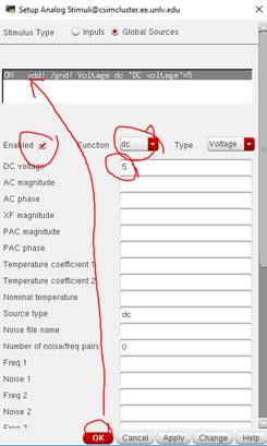
There is no output due to there not being a “vdd!” source. Adding a vdd!
Instance to the schematic (and also setting it in the ADE Setup -> Stimuli):
Note: The Stimuli is basically a global
“power supply” that will artificially add voltages to input/global sources.
Rerunning the
Simulator using the saved state and Result:
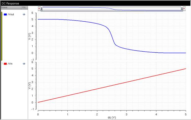
The Inverter with a Power
supply “VDD!” (Good :)
The Schematic
is a success!
Now to
simulate the Extracted Layout:
 (Using ADE Setup -> Environment)
The Inverter with a Power
supply “VDD!”, Extracted
Verify that
the Extracted Layout is simulated (Using Simulation -> Netlist ->
Display):
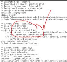
This finishes
up Tutorial 3 and the Prelab.
-------------------------------------------------------------------------
Lab:
Experiment 1: Schematic,
Layout, and Symbol for a 12μ/0.6μ PMOS and 6μ/0.6μ NMOS
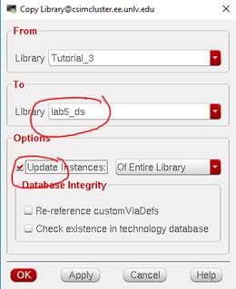
Copy/Paste
from Tutorial_3 to lab5_ds:
Schematic of the
12/6 PMOS-NMOS inverter, and add input pin A and output pin Ai:
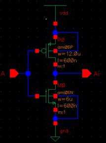
Check and save
the schematic.
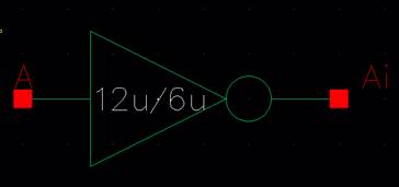
Creating/editing
the symbol for this inverter to use in another schematic (Create -> Cell
View -> From Cell View):
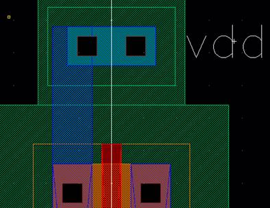
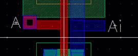
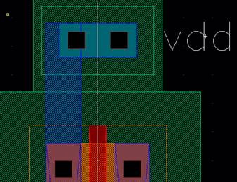
Laying out the
Inverter:

DRC the
connections:

Add some blue
rectangle metal1 pins, where A is an input, Ai is an output.
DRC the
layout.
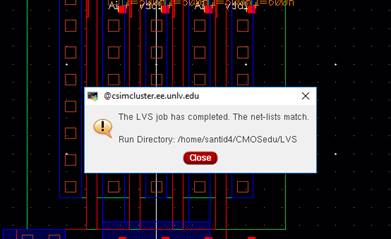
Extract the
layout, and LVS the extracted layout:
It passes the
LVS.
NOTE: Simulation
will be done in Experiment 3.
-------------------------------------------------------------------------------
Experiment 2: Schematic,
Layout, and Symbol for a 48μ/0.6μ PMOS and 24μ/0.6μ NMOS
(Using m=4):
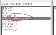
Rename the
inverter schematic from experiment 1 into “inverter_12uPMOS_6uNMOS”
Copy/Paste the
schematic into “inverter_48uPMOS_24uNMOS”:
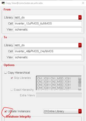
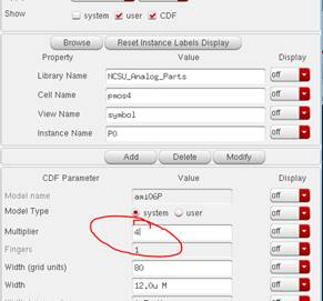
Changing
Multiplier to M=4:
Schematic:
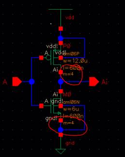
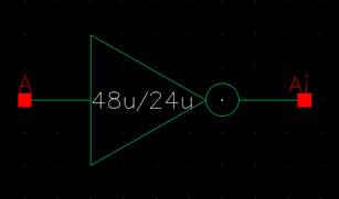
Symbol:
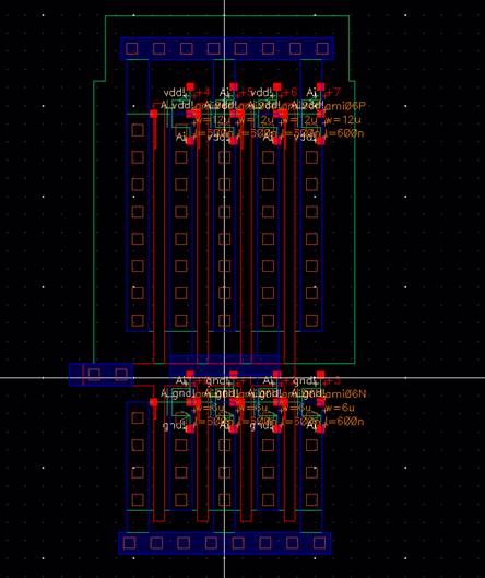
Laying out the
Inverter:
Complete
Layout:
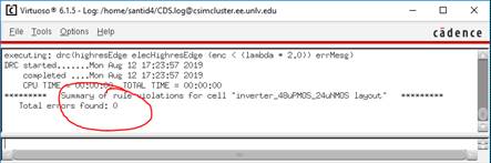
Complete
Extracted View:
Run LVS:
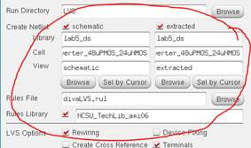
Passes LVS:
Experiment 3: Simulations 1
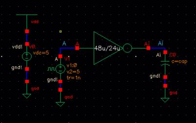
Simulating the
12μ/6μ Inverter first, here is the following schematic:
Launching the
ADE, adding the model libraries, and doing a transient response:
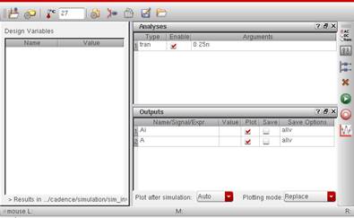
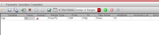
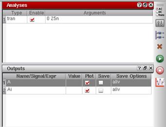
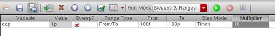
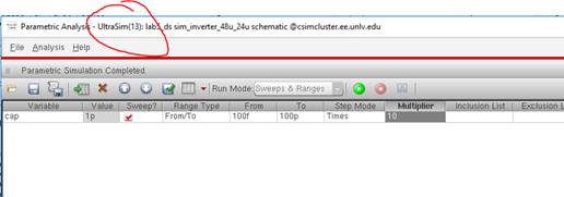
Using
Parametric Analysis with the Variable cap:
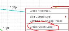
Creating
labels by right-clicking the mouse button and click “Create Graph Label”:
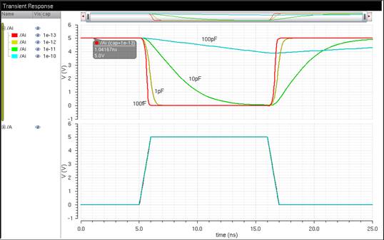
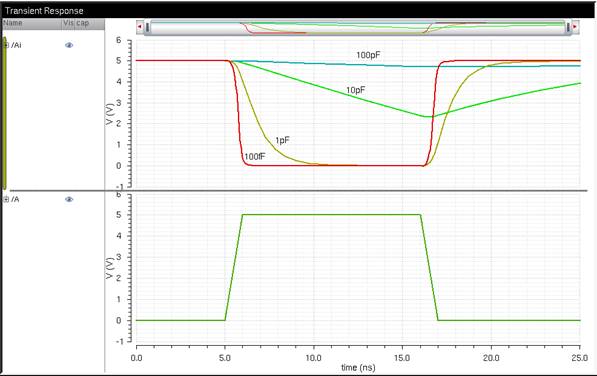
Finally,
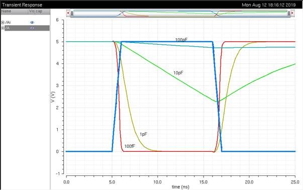
The 12u/6u Inverter, VDD from 0 -> 5V, And Varying Capacitors
From looking at
this, we can see that as the input is “Low”, the output is “High”, and vice
versa. The rise and fall time of the output is a bit longer than the input.
Also, the higher the capacitance, the longer the rise/fall time.
Simulating the
48μ/24μ Inverter:
Creating a new
strip by right-clicking a white space under “Name”, and clicking Split Current
Strip:
Finally,
The 48u/24u Inverter, VDD from 0 -> 5V, And Varying Capacitors
Now looking at
this, we can see that we still get that “inversion” effect with this inverter
schematic. However, with the bigger size, we get a huge gain (faster rise/fall
time).
With the
higher capacitances, they all have faster fall times compared to the
12μ/6μ inverter.
Experiment 4: Simulations 2
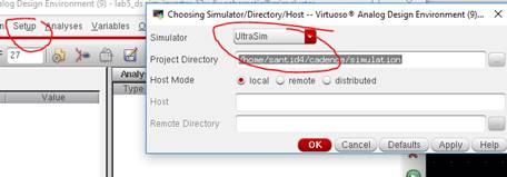
We will redo
the simulations using UltraSim.
12μ/6μ
Inverter:
The 12u/6u Inverter, Varying Capacitors in UltraSim
Looking at
this, it looks mostly the same as with the default simulator.
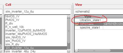
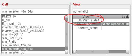
Saving this results with a new UltraSim_state1 view, verifying that
we did it correctly:
48μ/24μ
Inverter:
Also notice
when using Parametric Analysis, you can see the UltraSim
Title at the top:
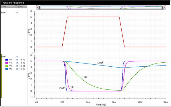
The 48u/24u Inverter, Varying Capacitors in UltraSim
And just as
with Spectre, we get the same results; Bigger MOSFETs
give us faster fall times and higher gains.
This concludes
Lab5.
NOTE: The files used in this lab can be downloaded
here.
--------------------------------------------------------