Lab 4 – IV Characteristics and layout of NMOS and PMOS devices in ON’s
C5 process
EE 421L Digital IC Design
Lab Date: 9/18/19 Due: 9/25/19
Last Edited on
9/24/19 at 3:32pm using Word
In this lab,
we will be characterizing MOSFETs and making a layout of an NMOS and PMOS.
For the
prelab, we will be looking at Tutorial 2.
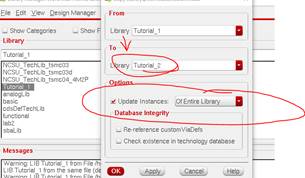
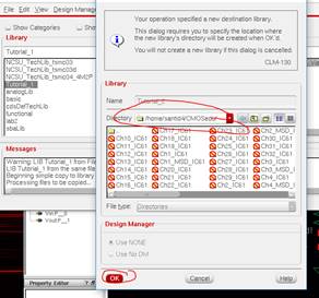
Copying all of
Tutorial 1 (created from tutorial 1) into a new Tutorial 2 Library:
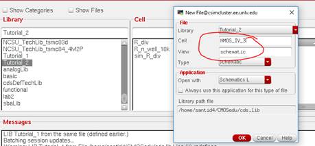
Creating a new
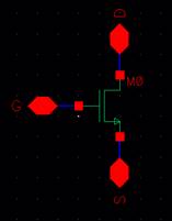
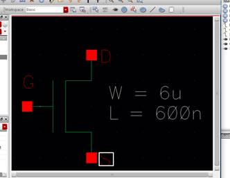
schematic in Tutorial 2 called “NMOS_IV_3” (3 as in 3 terminal MOSFET):
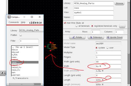
Creating a new
Instance, and choosing an NMOS from NCSU_Analog_Parts
-> N_Transistors -> nmos:
Creating wires
and pins:
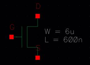
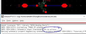
Checking and
Saving the schematic, creating a new symbol for this schematic by pressing
Create -> Cell View -> From Cell View
Deleting
everything and redrawing the MOSFET using the line shape and text shapes
(Create -> Note -> Text):
Check and Save
this symbol. Close it.
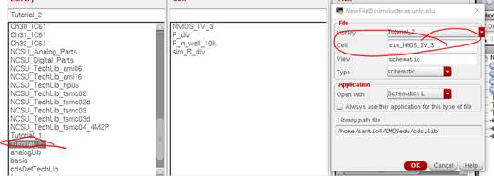
Now in the
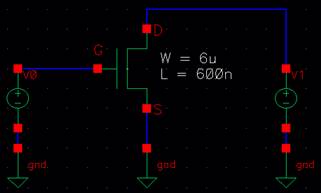
Tutorial 2 Library, create a new schematic, sim_NMOS_IV_3.
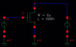
Instantiating
the NMOS_IV_3 symbol into the new schematic and creating the following:
Going back to
the symbol, move the labels so they are not on the wires.
Check and
Save, close it.
Going back to
the schematic:
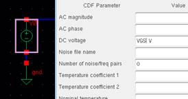
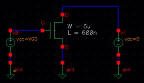
Changing the
DC voltage of the Gate to VGS and the DC voltage of the Drain to 0V:
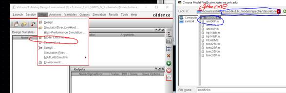
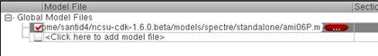
Launching the
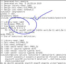
ADE, and in the ADE, do Setup -> Model Libraries and navigating to the
following:
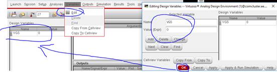
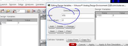
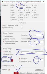
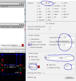
In the ADE,
going to Variables -> Edit, add the variable name VGS (the gate voltage that
will turn on the NMOS) and a Value 0.
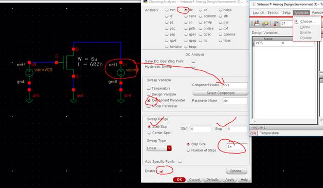
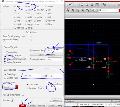
In the ADE, go
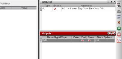
to Analyses -> Choose and set the following below:
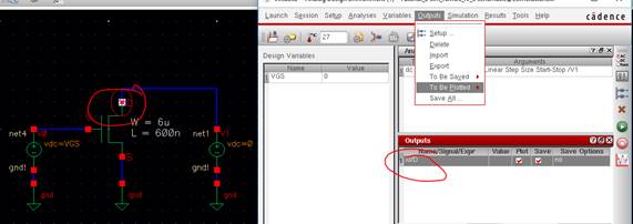
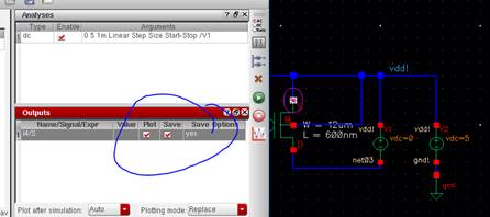
Now do Outputs
-> To be Plotted -> Select on Schematic, and
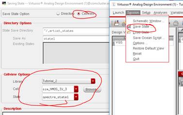
click on the “D” pin so that we can plot the current.
Save this
simulation state.
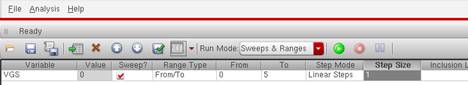
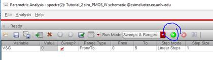
In the ADE,
Tools -> Parametric Analysis, set up the following:
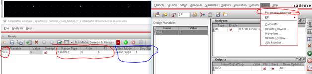
Press the
Green Start Button in the Parametric Analysis.
Close the
Output window, save the ADE State, and close the Simulator.
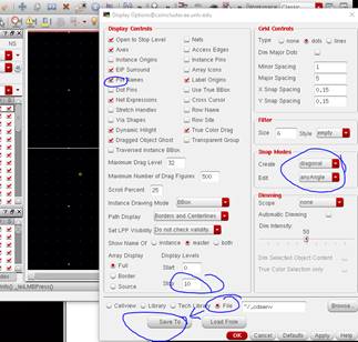
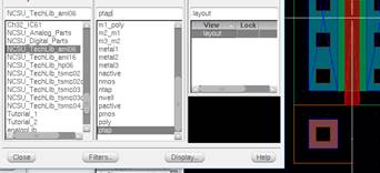
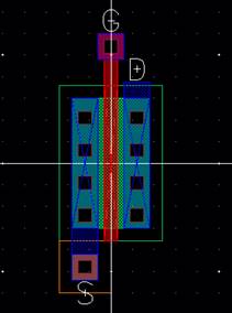
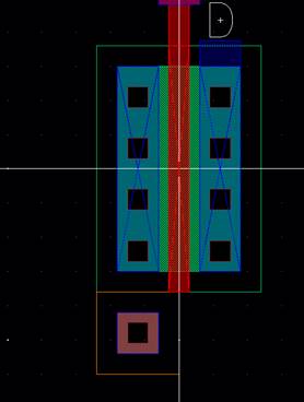
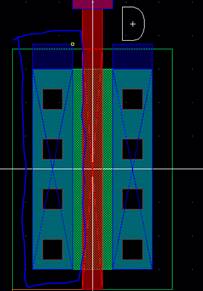
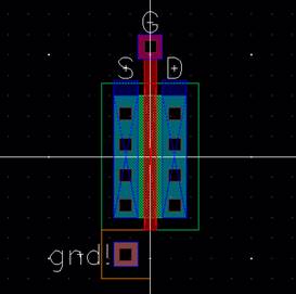
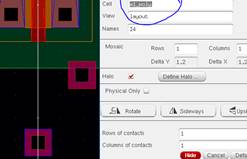
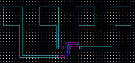
Laying out the NMOS:
In the Library
Manager, create a new layout for NMOS_IV_3 (not the sim schematic).
The defaults
are usually loaded for the display. Press bindkey e,Set up the following parameters,
and save these options to a file.
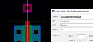
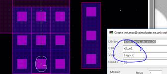
Create a new instance
for an NMOS:
Instantiate a ptap cell and place it as shown.
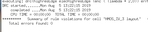
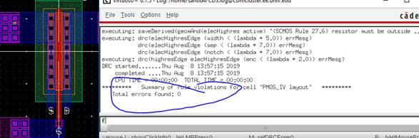
Run the DRC.
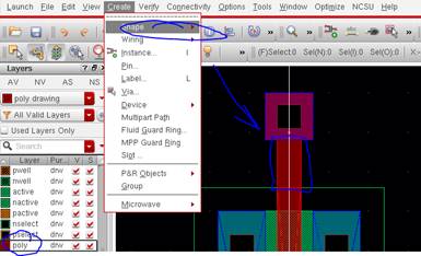
Now, lets add a m1_poly layout piece to the top of the gate of
the NMOS.
In the poly (drw) layer, draw a rectangle from the gate poly piece to
the bottom of the m1_poly layout.
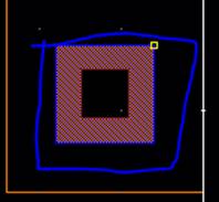
Adding
rectangles to connect the ptat square and a 2nd
rectangle on the right to go above the NMOS.
I have a
spacing error:
Using a ruler,
reshape the rectangle.
Create Pins
(on metal1 layer):
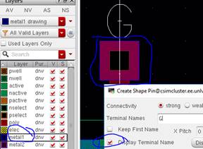
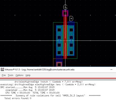
DRC the
layout.
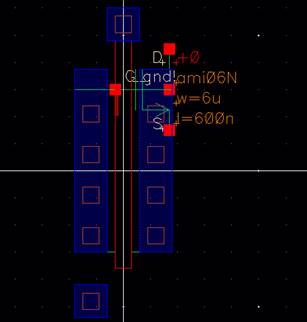
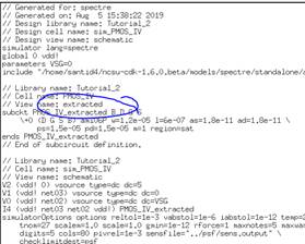
Now extract
the layer (Verify -> Extract). Open the extracted file.
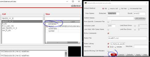
Extracted
View:
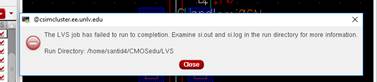
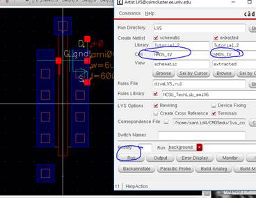
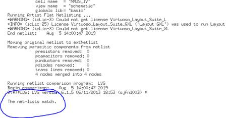
In the
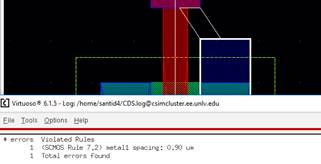
extracted window, run an LVS (Verify -> LVS).
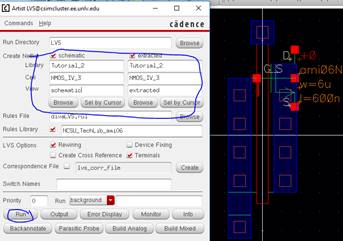
The LVS fails
the run:
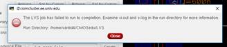
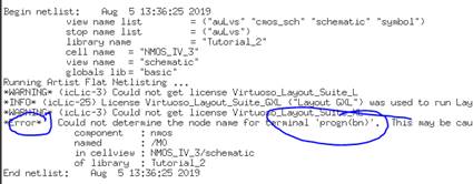
In the LVS
menu, pressing on Info -> Log File, and we will get the error:
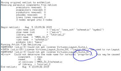
We need to
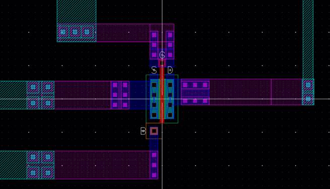
modify the NMOS layout a bit so that we can connect the body of the PMOS.
Going back to
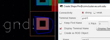
the NMOS layout, delete the S pin and the metal1 rectangles.
Adding a few
rectangles:
DRC again:
Add some more
pins:
Run another
DRC and save.
Now extract
the layout again (Verify -> Extract). Open this new extracted file.
Run the LVS
again.
It failed.
We need to
have a 4 terminal NMOS so that we can connect the body to gnd!
Close the
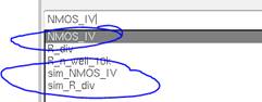
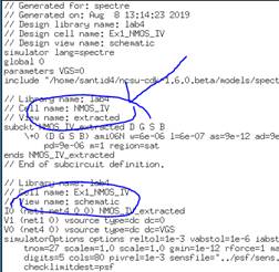
extracted window, layouts, and in the Library Manager, rename “NMOS_IV_3” to
“NMOS_IV”, and also for the sim file.
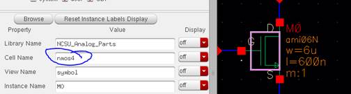
Open the
NMOS_IV schematic, and replace the nmos
instance with nmos4 (Click on NMOS, bindkey Q, and
rename).
Add a wire to
the body, and label it “gnd!”.
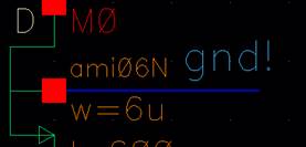
Check and
Save.
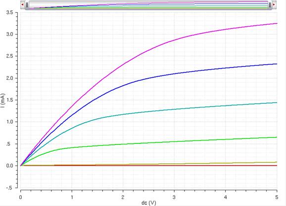
Resimulating with the new schematic by Loading our
previous state (Running the ADE L in sim_NMOS_IV, and
loading state from a cell, then using Tools -> Parametric Analyis):
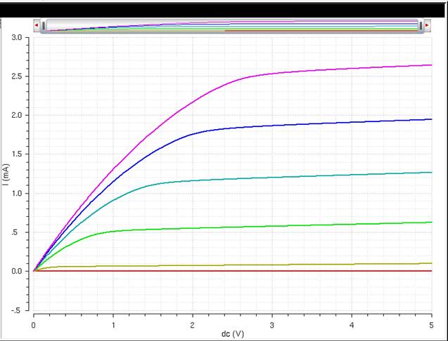
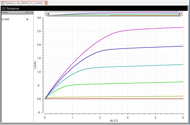
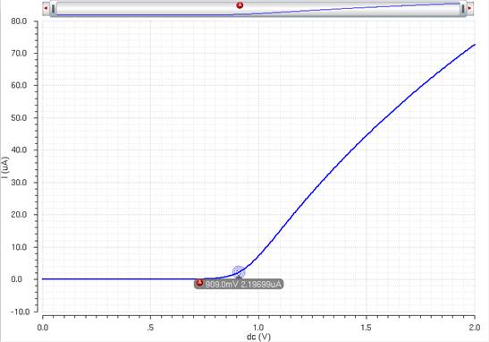
NMOS IV Curve, With Varying VGS
Close the
sims.
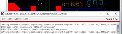
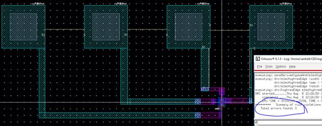
Reopen the
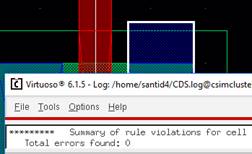
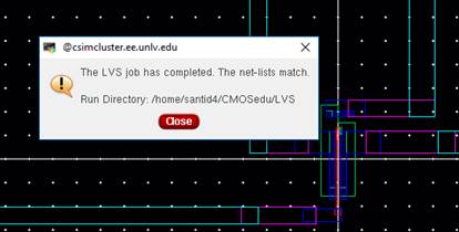
Extracted Layout, and run the LVS again.
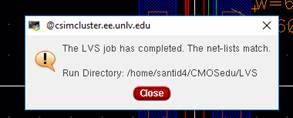
The LVS run
passed:
Now in sim_NMOS_IV again, run the simulation and load the state
again.
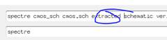
Now to sim the
extracted view, go to Setup -> Environment and type “extracted” in front of
“schematic”.
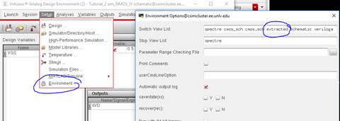
Click OK, and run the Parametric Analysis again.
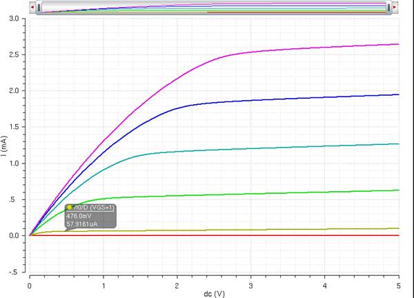
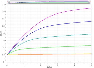
NMOS IV Curve, With Varying VGS, Extracted
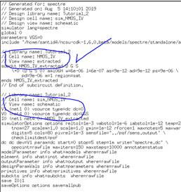
It’s the same
thing. To make sure we are running the Extracted layout, go to Simulation ->
Netlist -> Display and the extracted file comes on top of the netlist:
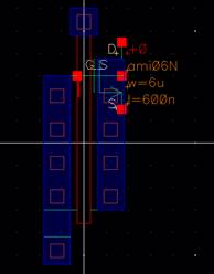
We are done with the NMOS and we can now do the same for the PMOS.
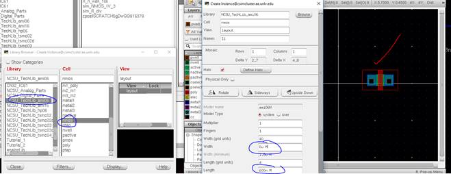
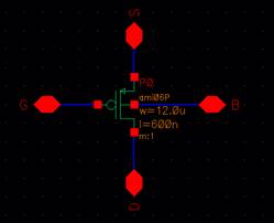
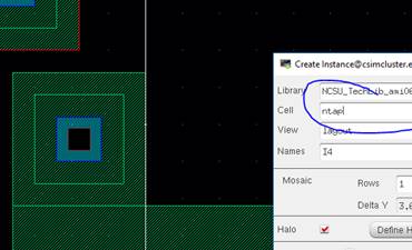
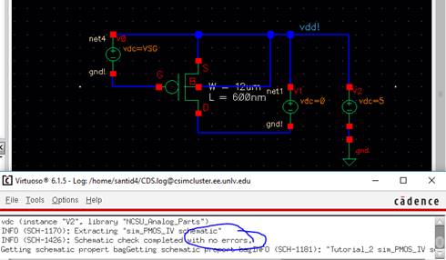
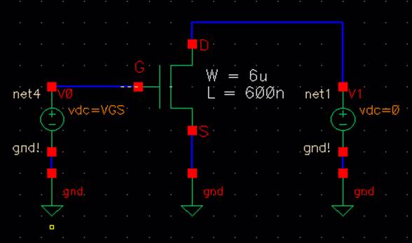
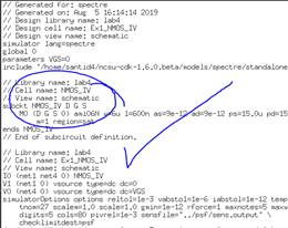
Lets make a new schematic cell view “PMOS_IV” with the pmos4 component
(With W=12μ and L=600n):
Check n Save:
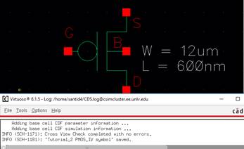
Create a new
symbol (Create - > Cellview -> From Cell View).
Create the following, and check and save it.
Create a new
Layout:
DRC and Save
it.
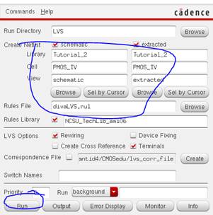
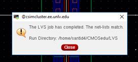
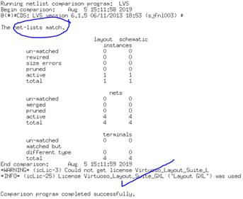
Extract the
Layout, and then open the new extracted file. Run the LVS.
Now create a
new cell, “sim_PMOS_IV” and create a new schematic.
Check and Save.
Launch the
ADE, from scratch, load up the Model Library (Setup -> Model Libraries) and
add the following:
Add Variables:
Going to
Analyses -> Choose:
Doing Outputs
-> To Be Saved -> Select on Schematic, and click on the S pin:
Save this
State.
Doing Tools
-> Parametric Analysis, and pressing on Run:
Result:
PMOS IV Curve, With Varying VGS
Simulating the
PMOS Layout by going to Setup -> Environment, and
typing “extracted” in front of “schematic”.
Resimulating:
PMOS IV Curve, With Varying VGS, Extracted
Verifying that
the extracted layout is being simmed by going to
Simulation -> Netlist -> Display:
Close and save
everything.
This ends
Tutorial 2 and the prelab.
-------------------------------------------------------------------------
-------------------------------------------------------------------------
Lab:
Experiment 1: ID v. VDS of an
NMOS, VGS from 0 to 5V (1V step) and VDS from 0 to 5V (1mV step) using
6μ/600n Ratio
Running the
ADE with a DC sweep (Parametric Analysis):
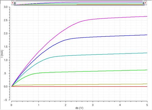
NMOS IV Curve, With Varying VGS
Experiment 2: ID v. VGS, VDS =
100mV, VGS from 0 to 2V (1mV step)
Copying and
saving the previous schematic into a new cell, “Ex2_NMOS_IV” (and changing the
schematic):
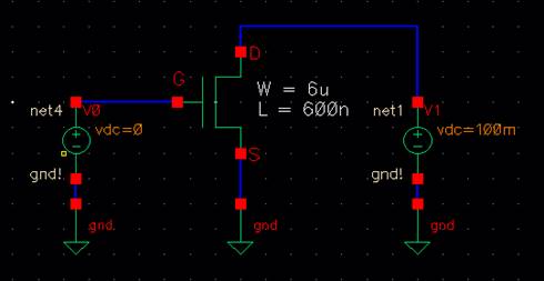
Launching the
ADE, and creating a new state:
Pressing on
the Green Arrow Key to simulate this circuit:
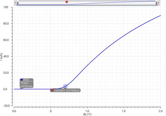
NMOS IV Curve, Id vs. VGS, Constant VDS
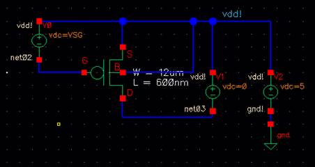
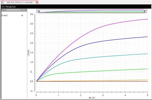
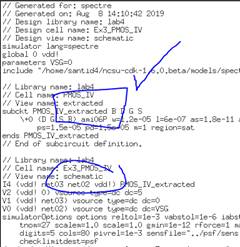
Experiment 3: ID v. VSD of PMOS
with VSG from 0 to 5V (1V Step) and VSD from 0 to 5V (1mV step) with
12μ/600n Ratio
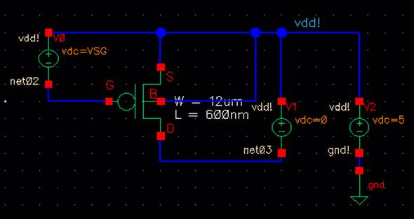
Running the
ADE, DC sweep on VSD and Parametric Analysis on VSG:
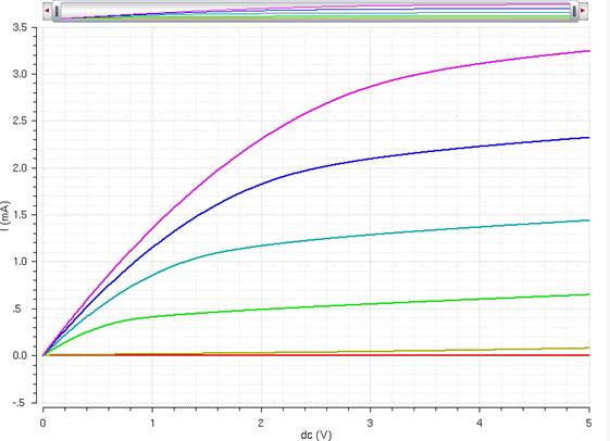
PMOS IV Curve, With Varying VSG
Verifying that
the Schematic is running (Simulation -> Netlist -> Display):
Experiment 4: ID v. VSG of PMOS
with VSD = 100mV, DC sweep VSG from 0 to 2V (1mV step).
Copying the
previous schematic into “Ex4_PMOS_IV” and changing the schematic values:
Launching the
ADE and creating a new state:
Running the
simulation:
PMOS IV Curve, Id vs. VSG, constant VSD
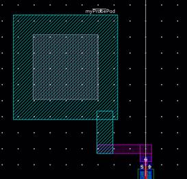
Experiment 5: Layout the NMOS
with Probe Pads
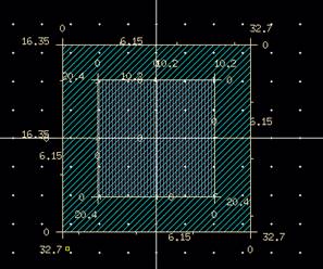
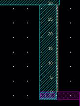
So from the MOSIS Layout Rules, for Pads:
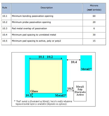
We should
create a bonding pad that on Metal3, the topmost layer.
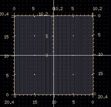
The Probe pad Glass will be around
20.4μmx20.4μm, about the center.
The Pad/Metal Overlap
passivation will be greater than 6μm, we will have 6.15μm for
personal preference.
Thus the Bonding pad will be 6.15 + 10.2 = 16.35μm, so the Metal3
layer is 32.7μmx32.7μm.
Let’s create
the Glass first. Using the ruler and the Glass layer to draw a rectangle.
Then, giving a
good “clearance” between the glass and Metal3 layer, we will do around
6.15μm of clearance.
Creating a
quick label on top of the pad:
Save this.
Now create a
schematic for the probe pad.
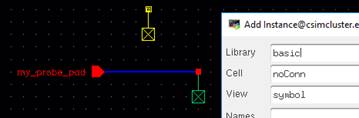
Create a
symbol (Create -> Cellview -> From Cellview):

Now let’s use
this symbol in the NMOS schematic (Plus, editing the gnd!
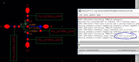
Pin and changing it to the Body and have 4 probes):
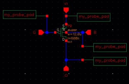
It passes the
Check and Save.
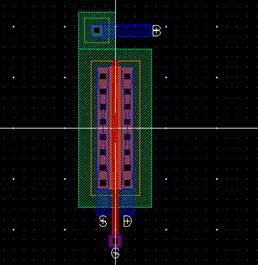
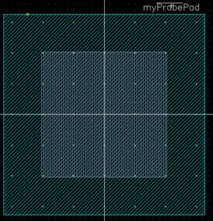
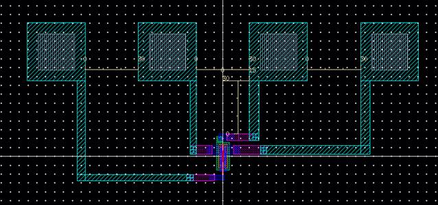
Now lets
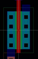
layout the pad with the NMOS (Using Metal3 and Metal2 connections):
 (Following 10.4)
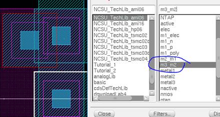
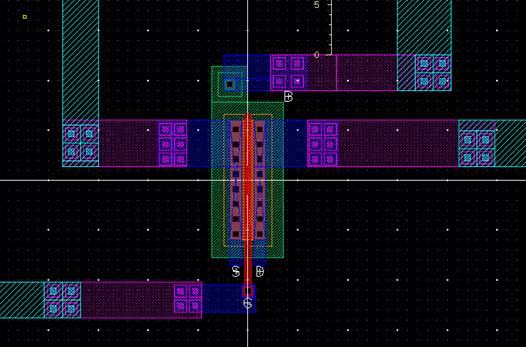
Closer view
(and changing gnd! To “B”):
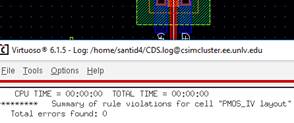
Passes DRC:
Extracted the
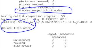
Layout:
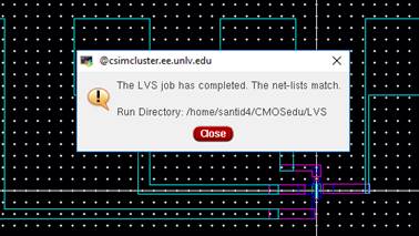
Run the LVS,
and it passes:
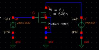
Rerun
Experiment 1 with the new layout (note the body has been connected):
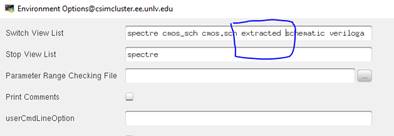
Load the sim
state, and in the ADE, Setup -> Environment, add the word “Extracted” in
front of “schematic” shown below:
The simulation
ran successfully with the probed NMOS layout:
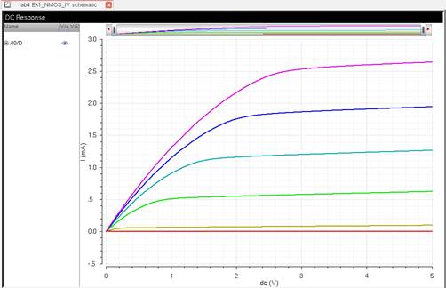
NMOS IV Curve, With Varying VGS, Extracted
Verify the
extracted layout is running first (Simulation -> Netlist -> Display):
Experiment 6: Layout the PMOS
with Probe Pads
This will be
the same approach as the NMOS.
Since the Pads
have already been made, we will go on laying out the PMOS.
Editing the
PMOS4 schematic with probe pads (and running Check and Save):
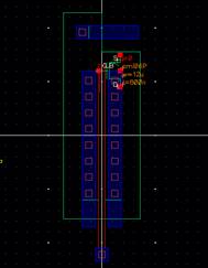
Placing pads
down in a PMOS created from Tutorial 2 (and DRCing
each pad one by one):
Close up view:
Entire layout
passes DRC:
Extract the
layout:
Run the LVS on
this extracted layout:
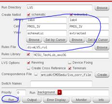
Passes LVS:
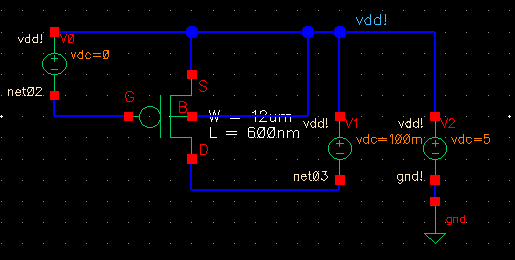
Rerun
Experiment 3 (ID v. VSD) with the extracted layout:
In the ADE,
Setup -> Environment, add “extracted” in front of “schematic”:
Run a
parametric analysis:
PMOS IV Curve, With Varying VSG, Extracted
Verifying the
Extracted layout is being simulated:
This concludes
Lab 4.