Lab 3 – Layout of a 10-bit Digital-to-Analog Converter
EE 421L Digital IC Design
Lab Date: Date# Due: Date#
Last Edited on
9/11/19 at 8:41pm using Word
From the
previous lab, we have designed and created a 10-bit Digital-to-Analog Converter
(DAC) schematic and linked the module to an Analog-to-Digital Converter (ADC). In reality, the circuit that we have designed needs to be
designed a little more detailed and needs a layout. A layout is basically one step closer for our schematic to
become a physical circuit that can be placed on a small (in the micrometer
range) chip.
We will need
to learn how to layout a simple circuit first, so for this, we will go back to Tutorial 1 (a schematic that has been
created in Lab 1) and layout the schematic that we have previously created. If
more details are needed in knowing how to create Tutorial 1’s circuit, refer
back to Lab 1.
Design Files
can be found here
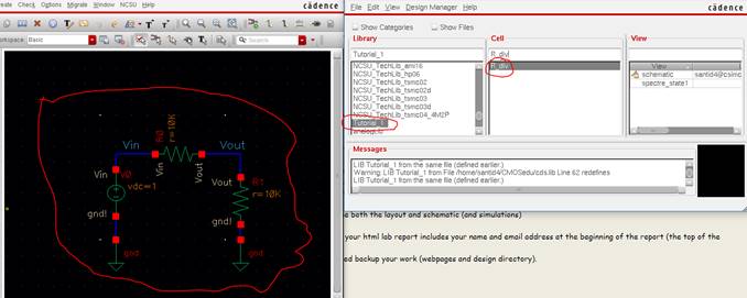
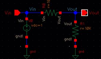
Let’s create a Layout for Tutorial 1: A Resistive Voltage Divider.
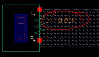
Open up Virtuoso’s Cadence Library Manager, and assuming
you have done Tutorial 1/Lab 1, Open up “Tutorial_1” in the Library Manager and
open the “R_div” schematic.
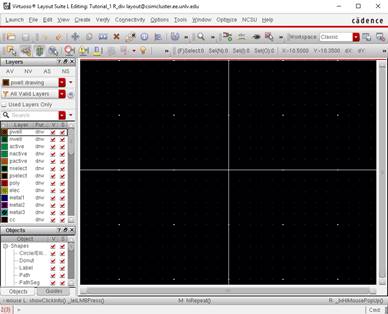
After creating
a new layout cell for R_div (highlighting R_Div, File -> New -> Cell View, and using Type =
Layout), this is what shows up:
Follow the
Rest of Tutorial 1:
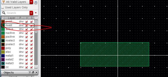
Clicking on
the “nwell” layer (with drw
as drawing layer), create a simple rectangle.
Clicking on
the rectangle, use bindkey q (or Edit -> Basic -> Properties) to edit the rectangle’s
properties.
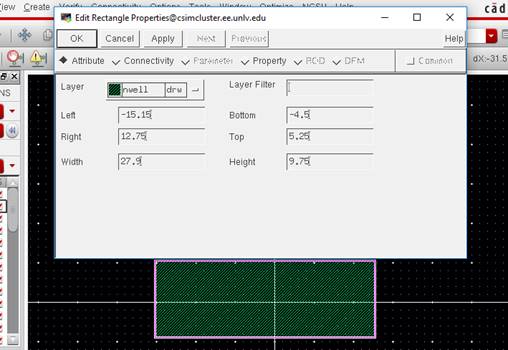
What Size Rectangle do we need?
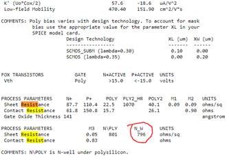
For the C5
process, the sheet resistance of an n-well is around 800Ω.
The minimum
width of the n-well is 12 lambda (lambda = 300nm) or 3.6μm.
Looking at the
C5 MOSIS parameters online, we can see that the square sheet resistance is 796Ω.
The Formula
for resistance in layout is:
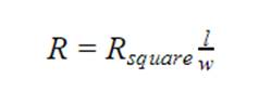
If we want to
use the minimum width of 3.6μm, solving for L with R = 10kΩ, Rsquare = 796Ω, and w = 3.6μm:
L = [ 10k x 3.6μ ] / 796 = 45.23μm.
This number
needs to be with regards to Lambda = 0.3μm, so we can divide that number
by lambda to get:
Multiples of
Lambda = 150.75 ≈ 151 lambdas
So L = 151 x (0.3μm) = 45.3μm.
And W = 3.6μm
Punching these
numbers into the properties (Left/Right = 22.65 and Top/Bottom = 1.8, negative
signs on Left/Bottom)
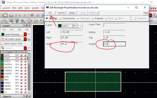
Click OK.
In the menu
(we will refer the menu as the Layout Window), click Verify -> DRC and on
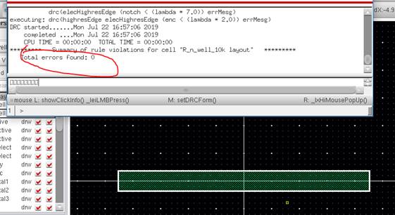
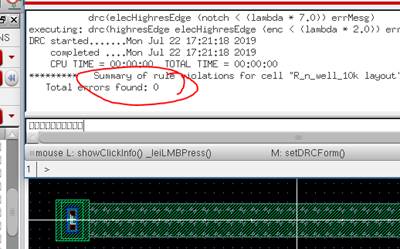
the next window, click OK to check the design for errors.
Since we did the
math with respect to the C5 process and its parameters, in this specific case,
we will have no errors (hooray for hand-calcs!).
How to measure the Length and
width of the resistor?
On the menu,
click Tools -> Create Ruler, click on one corner of the rectangle and to
another corner.
Using this
method, we will verify that our measurements that we placed into the
Rectangle’s properties are reflected in the layout window.
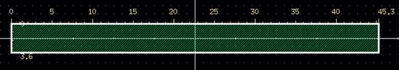
And yes, our
rectangle has a Length of 45.3μm and Width of 3.6μm
To delete the
ruler, go to Tools -> Clear all Rulers
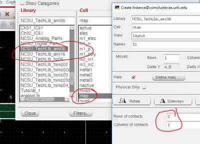
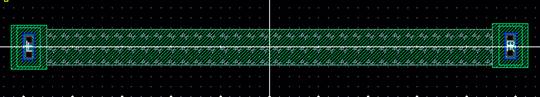
Lets add connections to the resistor. Click on bindkey
i in the menu to create an object, navigate the
Instance library for NCSU_TechLib_ami06 and find ntap.
Fill in the
Rows of Contact to be 2.
For this, I
will place the connectors at the left and right edges of the rectangle.
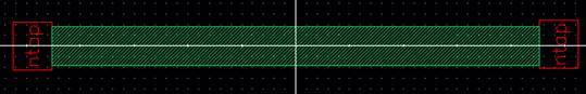
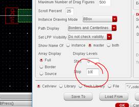
Going to
Options -> Display and Setting Stop = 10, we will se the outlines of nTap
Run the DRC to
make sure there are no errors.
Now for the
pins, in the menu, click Create -> Pin.
Change the
following:
Now, draw a
rectangle over the Ntap connector, and label the “L”
at the center.
Repeat with
the right side.
Doing a DRC
will return that L and R are on the same net (or wire). We will set the
resistance with the res_id layer (drw).
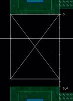
Just like before, create a rectangle around the long rectangle.
Doing a DRC
will return 0 errors.
To verify that
this is around 10kΩ, in the menu, click Verify -> Extract and click OK.
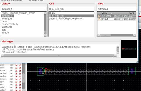
Going to the
Library manager, a new file, “R_n_well_10k” will appear. Open that file and
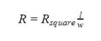
you’ll see the new layout below.
Zooming in, we
see that we have: 10.31kΩ.
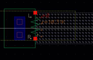
We have a +3%
Error. So we can fix this by “Solving” for Rsquare and then resolving for the new length.
With R =
10.31kΩ, W = 3.6μm, and L = 45.3μm, Rsquare
= 819.34Ω
Now solving
for L with R = 10kΩ and the new value for Rsquare:
L = [ 10k x 3.6μ ] / 819.34 = 43.94μm.
Dividing this
by lambda = 0.3μm, Multiples of lambda = 146.5 ≈ 147 lambdas = 44.1μm
Now our new
Left/Right = 22.05
Deleting the
Resistive layer and using Bindkey M to move stuff
around and relayering the resistor layer:
We now have a 0.3% error, and we have a resistance close to
10kΩ.
We are done
with this resistor, and can close the extracted view, and close and save the
R_n_well_10k layout.
To wrap up Tutorial 1, open
up the “R_div” cell schematic.
We will
instantiate 2 R_n_well_10k Layouts to our R_div
layout by pressing bindkey I, and
selecting that we want the layout of R_n_well_10k.
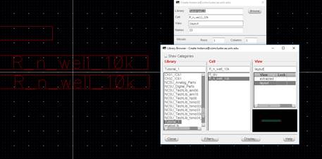
To actually view the resistors, in the Menu, Options ->
Display and set the Stop value to 10
Run the DRC.
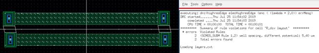
I get this
error, and to fix, place the resistors so that they are at the same X level,
but different Y level. To Solve for
this error, Cadence wants that the resistors should be at least 5.4μm
apart. Using a ruler (bindkey K), we can do this.
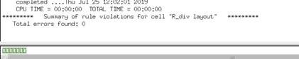
The DRC will
return 0 errors.
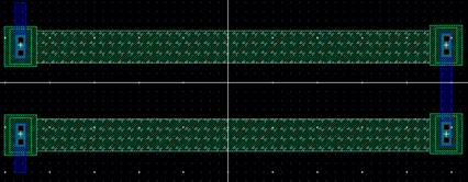
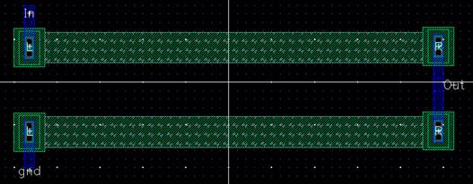
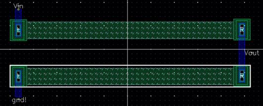
Select the
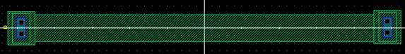
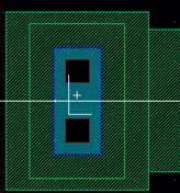
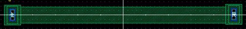
metal1 layer, and draw a rectangle from pin to pin
(the small little blue rectangles in the resistor).
Also, create
little “probing” pins to mark as the pin outputs and inputs.
Run the DRC to
make sure everything’ ok.
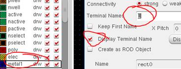
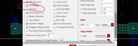
Press E to
open the Display settings, and make sure the “Pin Names” box is checked.
Create a Pin
by going to Create -> Pin, drawing a rectangle on metal1 drw
layer, and naming this pin “In”.
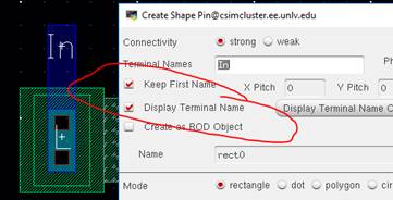
Repeat with
other pins “Out” and “gnd”.
Run the DRC.
Extract the
layout by Verify -> Extract.
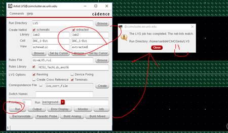
Now do Verify
-> LVS and type in the following and then press “Run”.
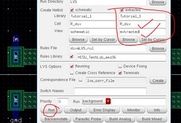
Click OK on
everything you see. You’ll Eventually run to an error that the pins did not in
the layout and schematic.
Press Output
from above picture to see the following:
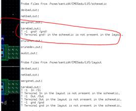
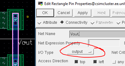
We will need
to then delete the pin names and rename them and set Vin and gnd! As inputs and Vout as
output.
Plus.. we will need to create an actual Vin and Vout pin in the schematic (I forgot to do this).
Redo the LVS.
This ends the
prelab.
--------------------------------------------------------
Laying out a 10-bit
Digital-to-Analog Converter (DAC)
In this
design, I will be using the R_n_well_10k resistors that was created in the
prelab to create a 1-bit DAC layout. This 1-bit layout will then be the
building block for everything else.
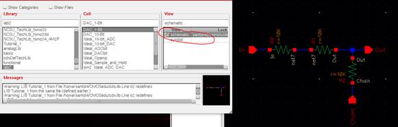
Opening up DAC_1-Bit schematic that I have made in lab2:
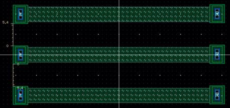
Creating Pins
(and setting their Input/Output properties with Bindkey Q):
Running the
DRC, Extracting this layout with Verify -> Extract,
and then beginning LVS with Verify -> LVS.
We can now use
this completed building block to build the 10-Bit DAC layout.
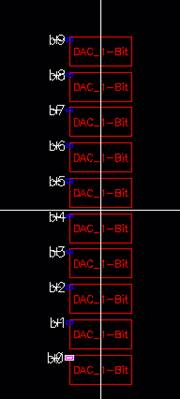
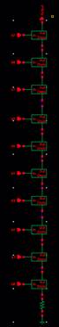
Clicking on
“DAC_10-Bit” schematic from the Library Manager and creating a Layout (by
instantiating the 1-bit DAC ten times):
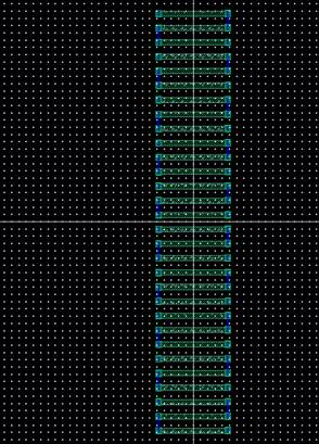
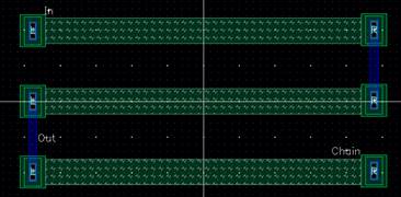
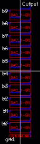
Now drawing
wires to connect them all.
Running DRC
(Passed):
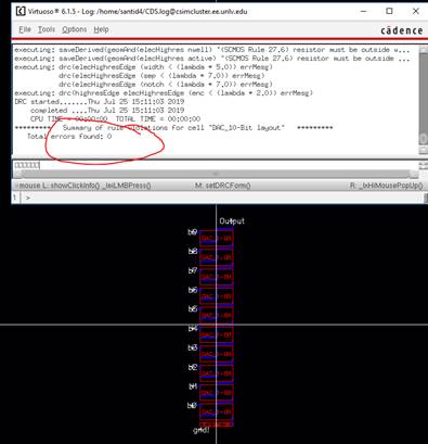
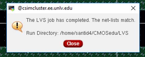
Extracting layout
and doing LVS:
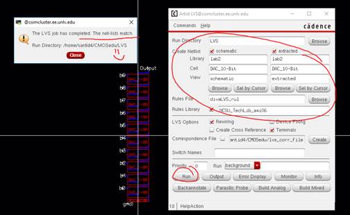
We have
finally successfully finished our layout.
Design Files
can be found here.