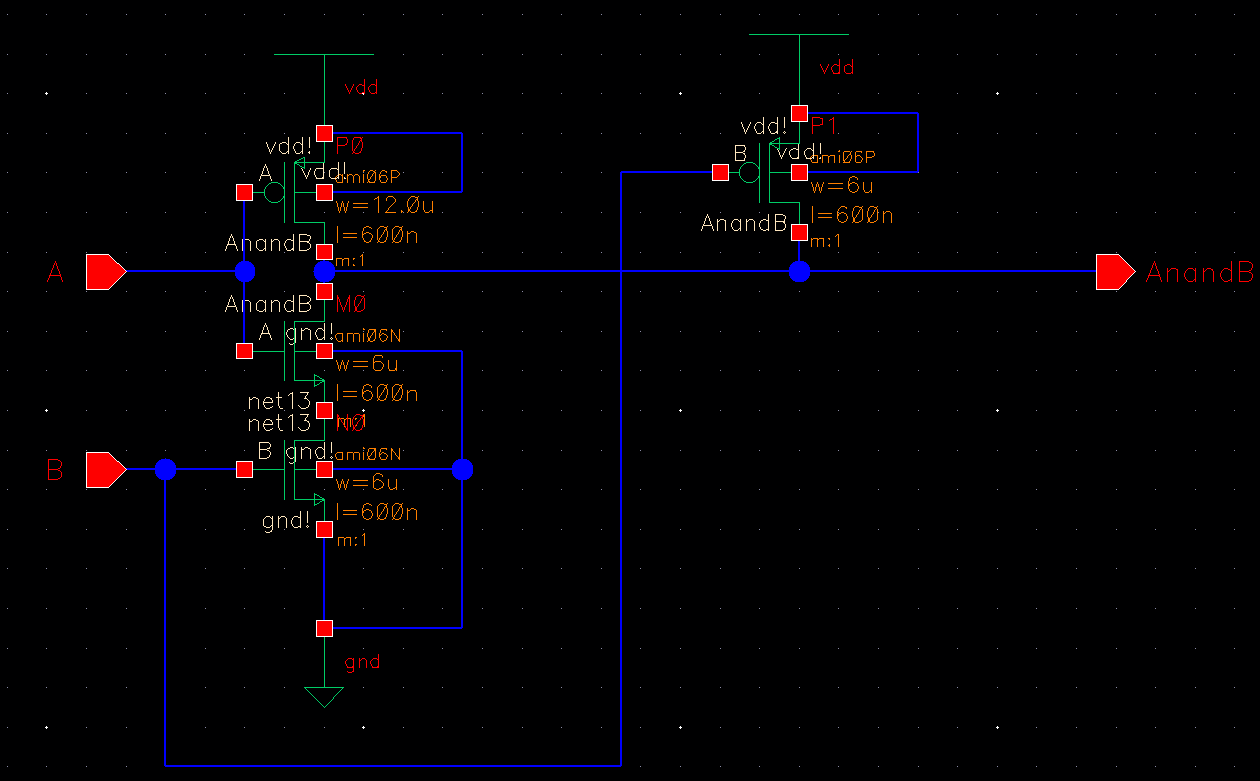
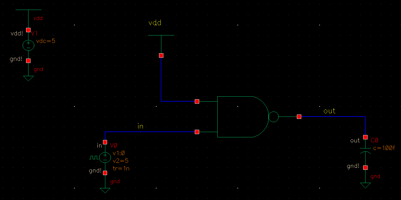
Below, we have the schematic for our CMOS NAND gate.
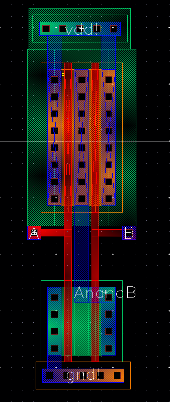
Here is the corresponding layout for our NAND gate...
Lab 6 - EE 421L
Actual Lab 6:
Here is the simulation schematic used for our NAND gate...
Here are the simulation results of our NAND gate
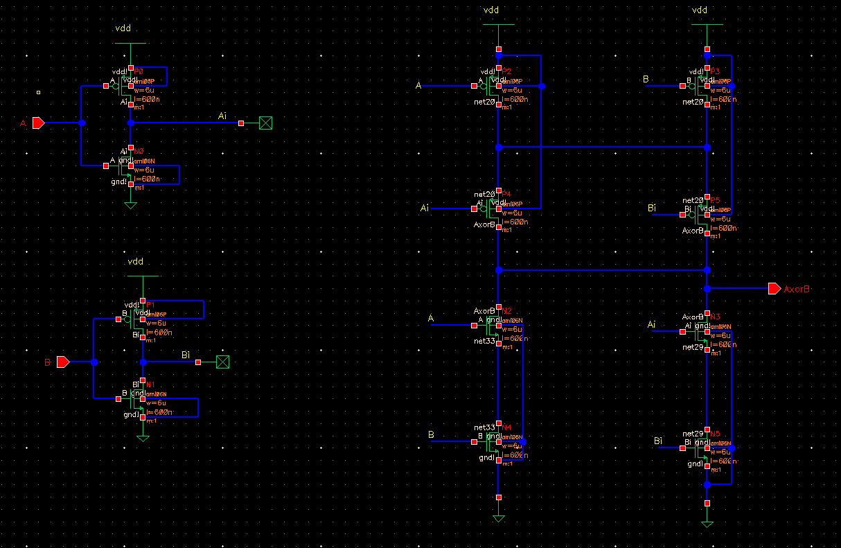
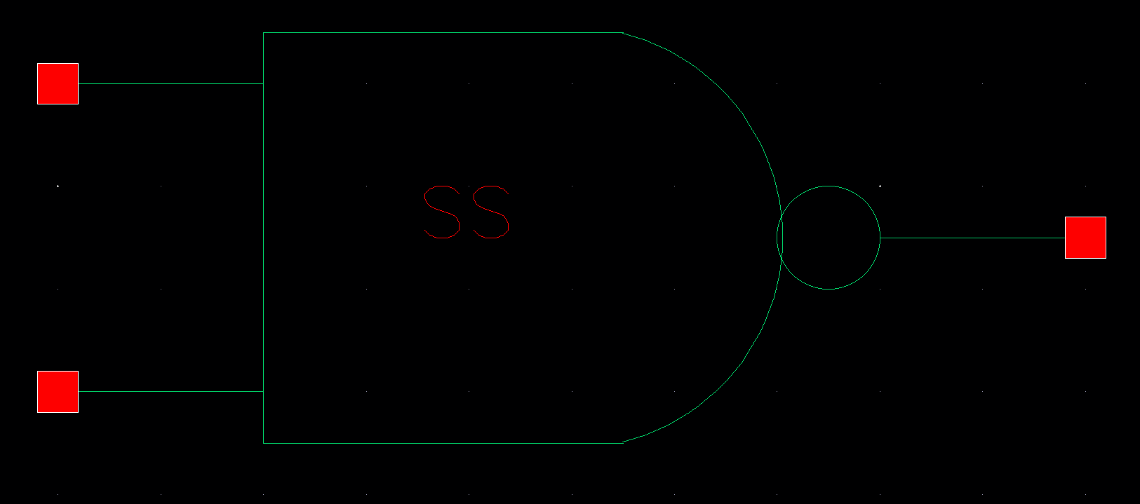
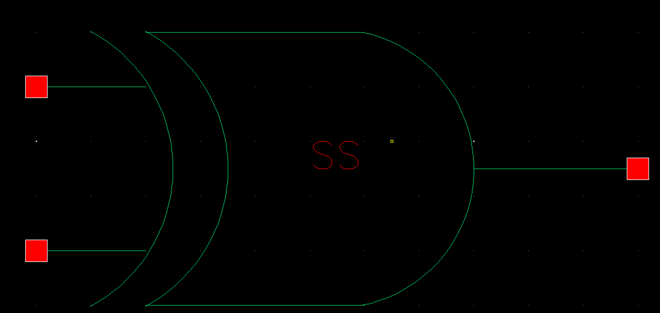
This is the corresponding XOR symbol...
Below is our XOR layout...
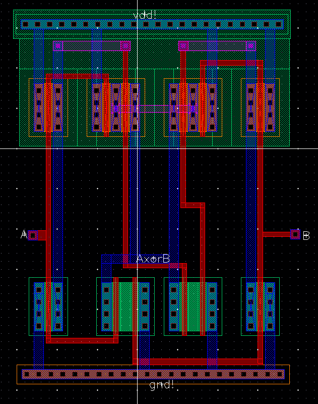
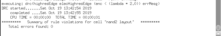
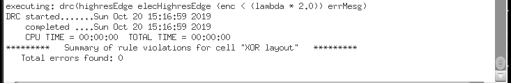
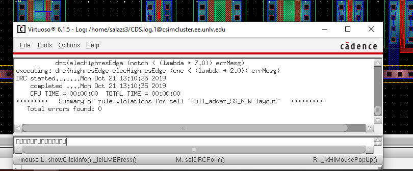
Our XOR layout under DRC nicely...
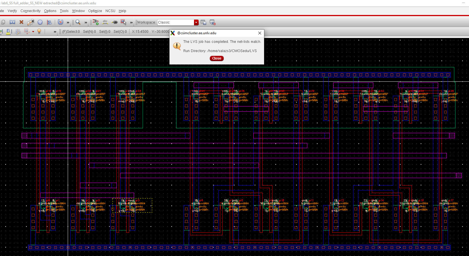
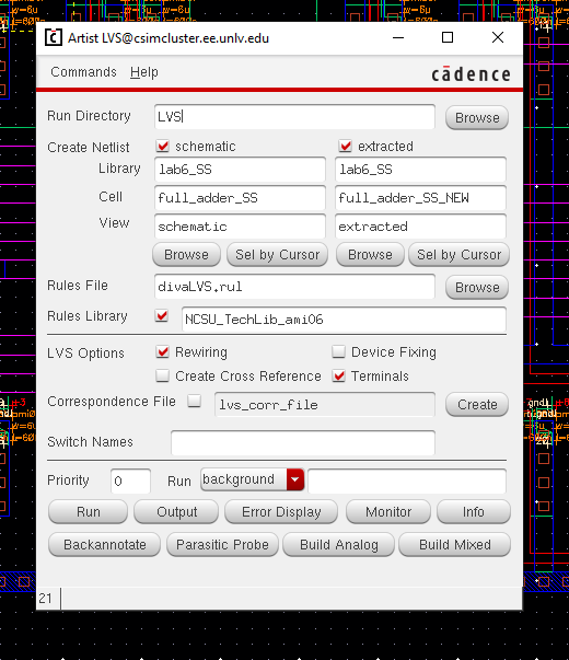
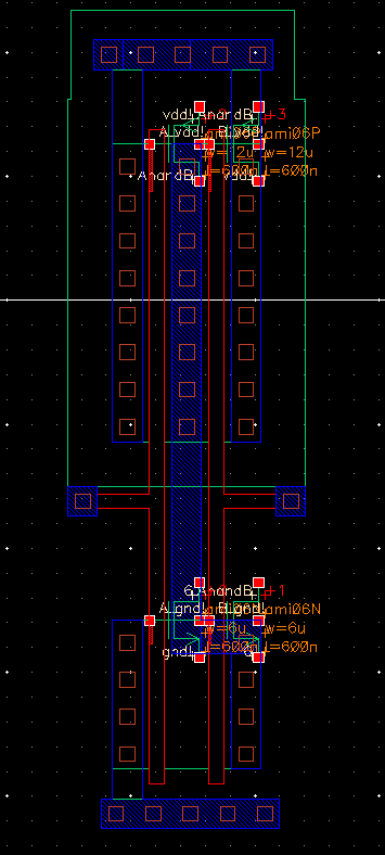
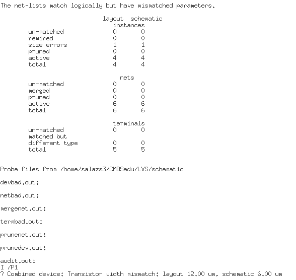
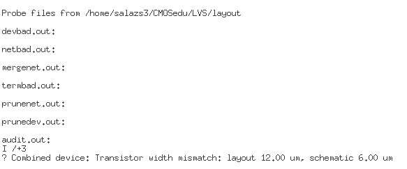
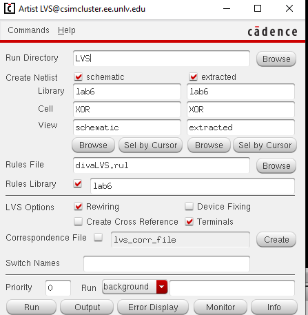
Here is the verification that our extracted view undergoes LVS very well...
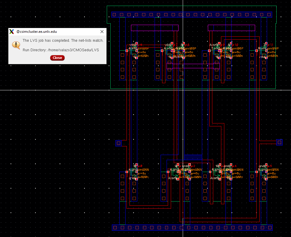
We can see the LVS window for the XOR layout below...
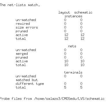
The net-lists match successfully...
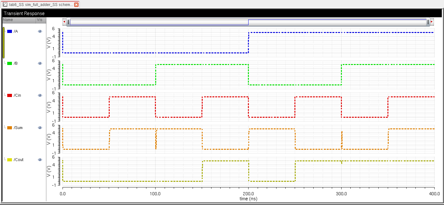
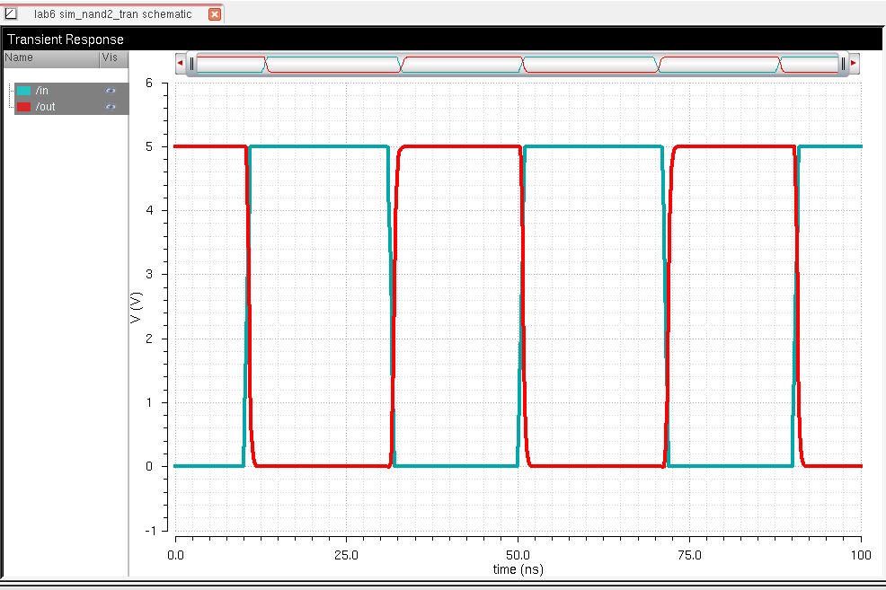
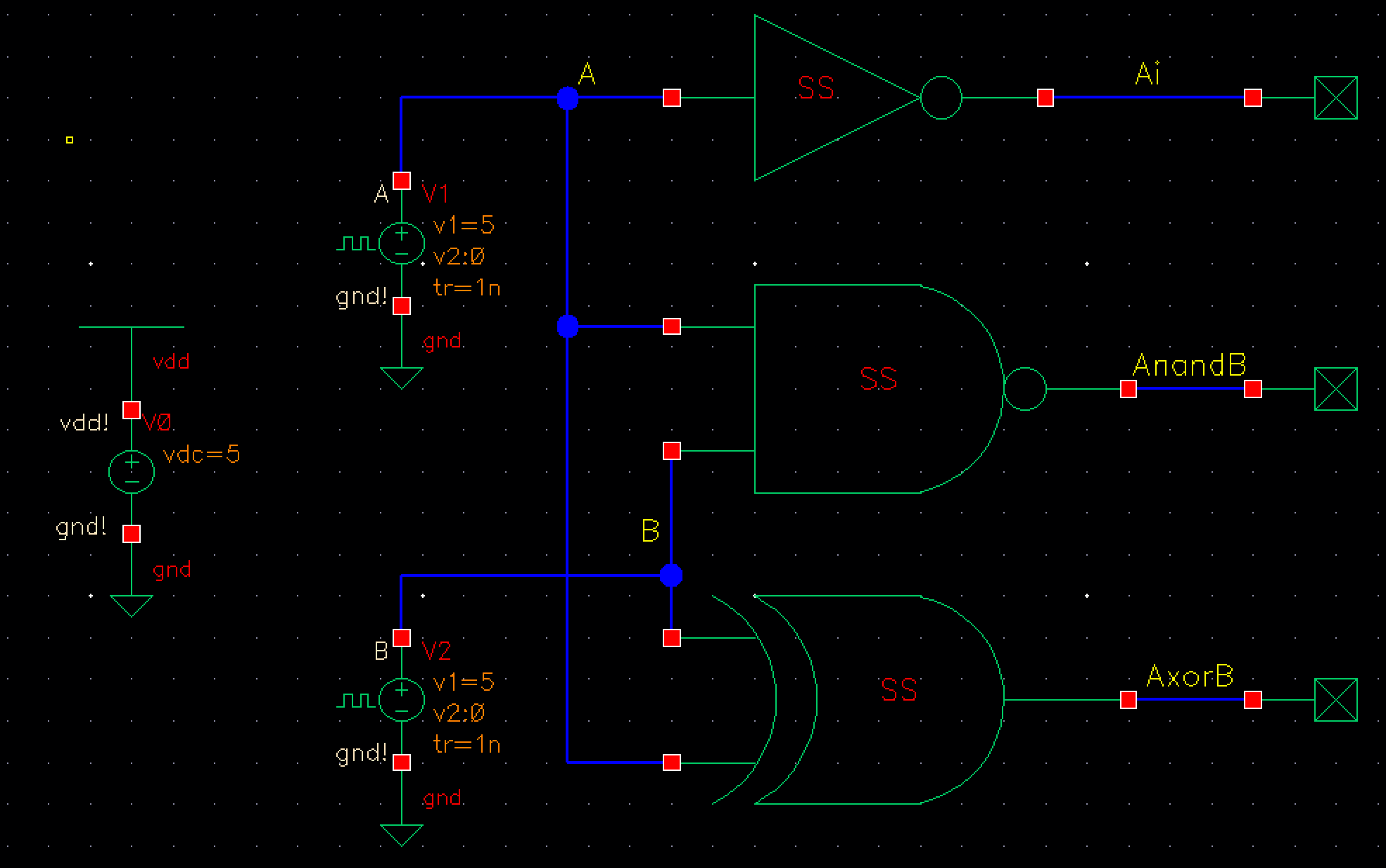
Below is the simulation schematic used to see how all of our gates work...
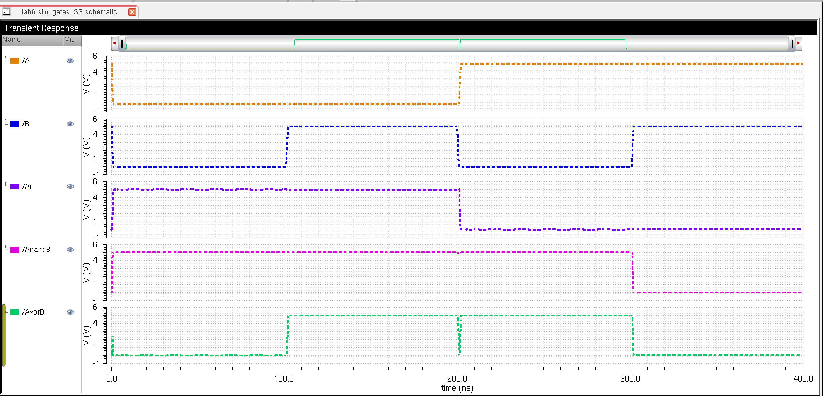
Here is our simulation results. After analyzing the results, we can see that the pulse signals that we have for our inputs create glitches at our rise/fall instances. This small yet important delay can point to having one gate having to delay outputting a correct signal before having another gate that is connected to this gate output another correct signal after a delay. This results in our glitches for our minute yet important to note glitches in our outputs.
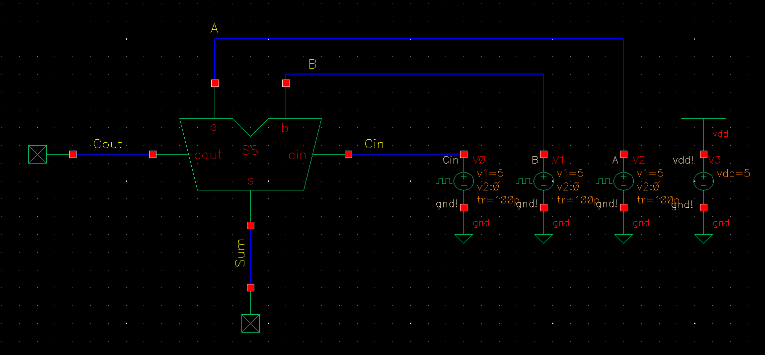
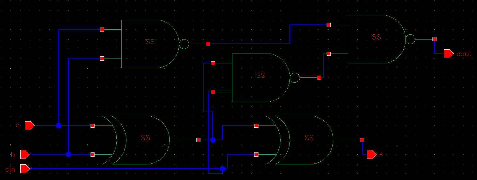
Below is the schematic for our full adder...
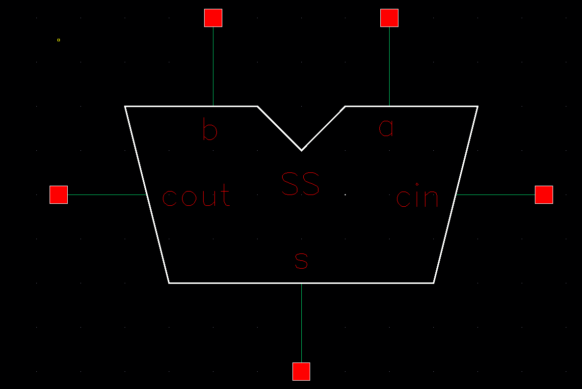
Below is our symbol for our full adder...
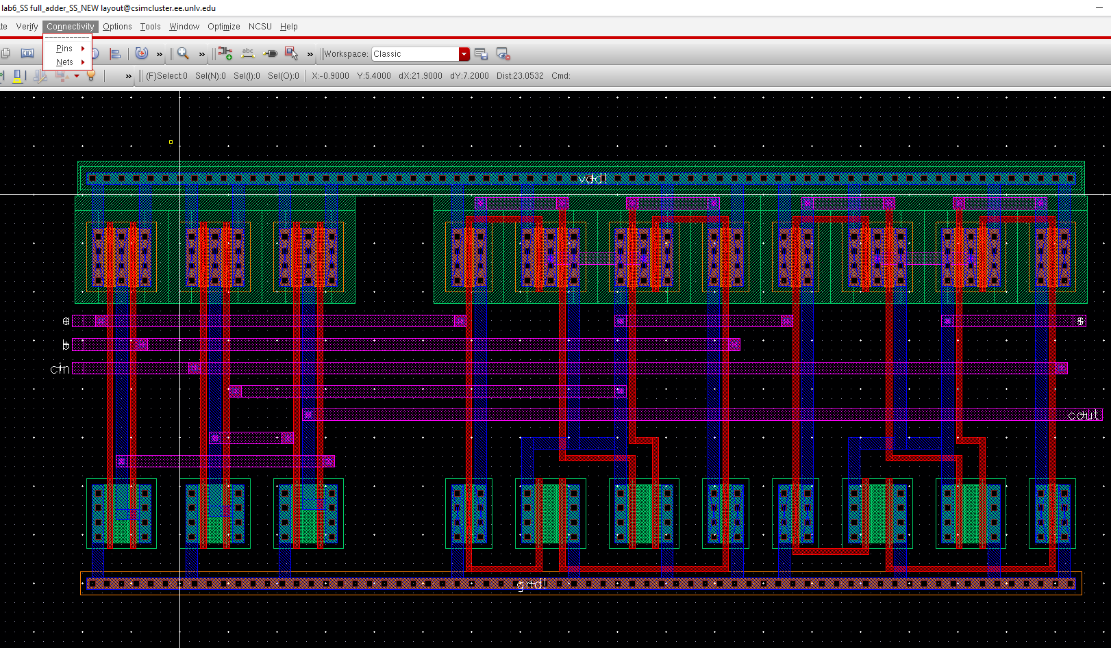
This is our layout for our full adder... we can note one particularly pesky LVS error was forgetting uppercase/lowercase pin texts matter...
Below is our extracted view with the accompanying window showing a successful LVS...