Lab 7 - ECE 421L
Using buses and arrays in the design of word inverters, muxes, and high-speed adders
All images can be double-clicked for larger versions
Prelab:
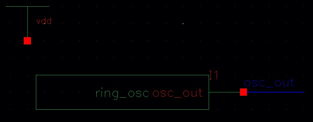
| Ring Oscillator | |
| Schematic | Symbol |
 |  |
| Layout | Extracted |
 |  |
| Sim Schematic | Sim Plot |
 | 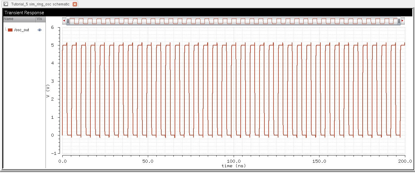 |
Make an equivalent, more concise, schematic by instantiating an inverter and naming the inverter using an arrayed name (I0<3:0>).
Connect a wide-wire (bus) and connect it to input and output pins. Create a symbol for the schematic.
| Schematic | Symbol |
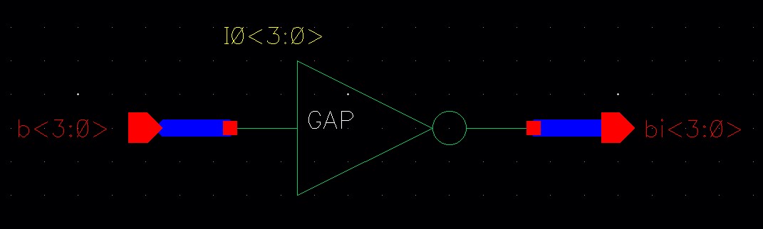 | 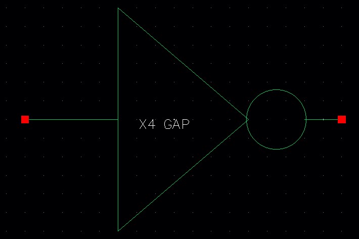 |
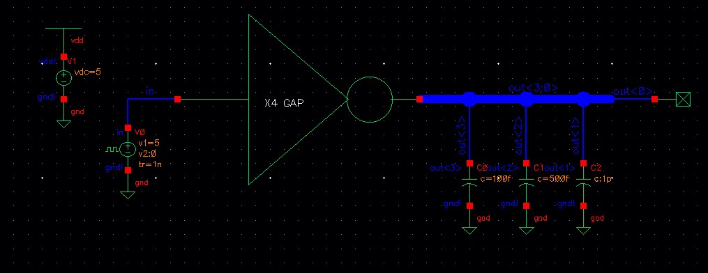
Using this symbol create a simulation schematic.
All four inverters' inputs are tied together to an input pulse source.
The out<0> is not connected to a load while out<3> is connected to a 100fF load.
The out<1> is connected to a 1 pF load while out<2> is connected to a 500 fF load.
| Schematic | Plot |
 | 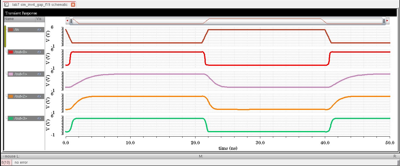 |
Being that the delay and rise/fall times rely on the time constant RC, we can see that as we increase the capacitor load from 0 to 1pF the time constant increasesand so do the delays and the rise/fall times.
Create schematics and symbols for an 8-bit input/output array of: NAND, NOR, AND, inverter, and OR gates.
| Schematics | Symbols | |
| NAND |  |  |
| NOR | 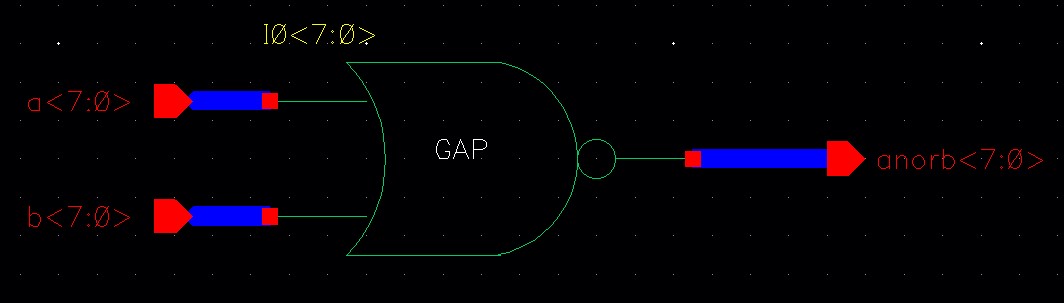 | 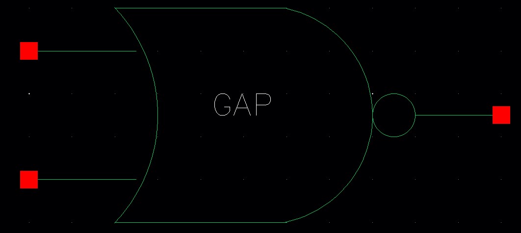 |
| AND | 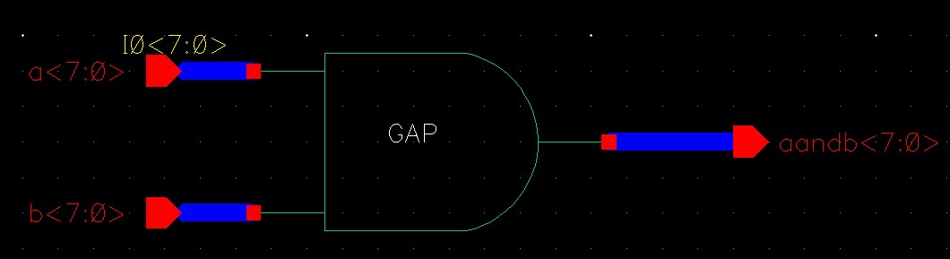 | 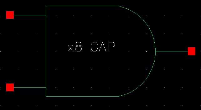 |
| INVERTER |  | 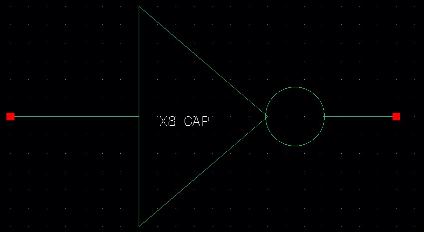 |
| OR |  | 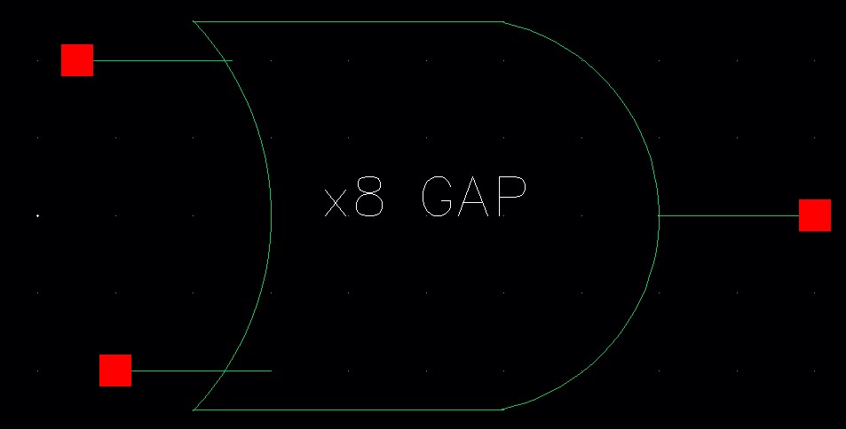 |
Provide a few simulation examples using these gates.
| Schematics | Plots | |
| NAND | 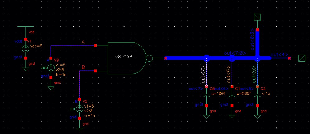 | 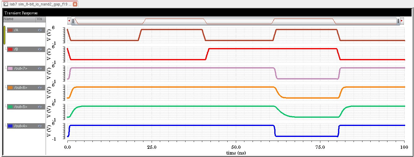 |
| NOR |  | 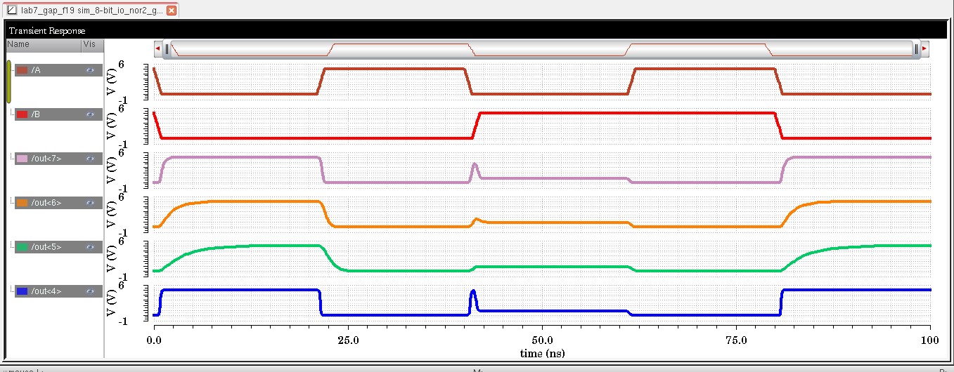 |
| AND |  |  |
| INVERTER | 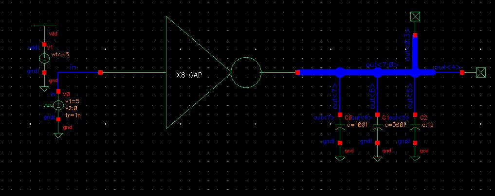 | 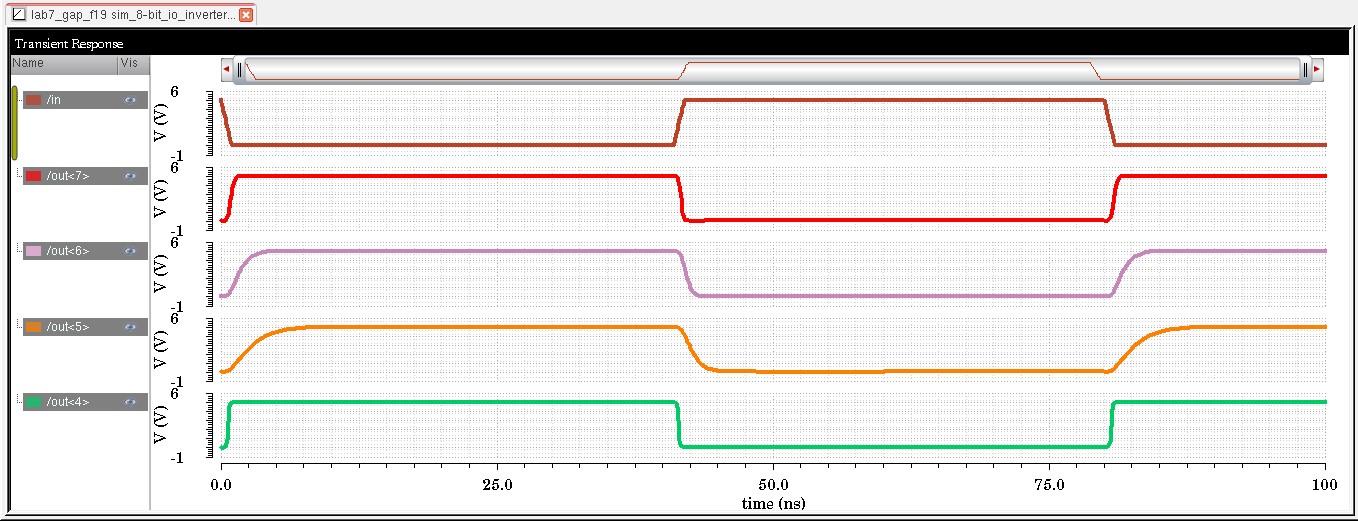 |
| OR |  |  |
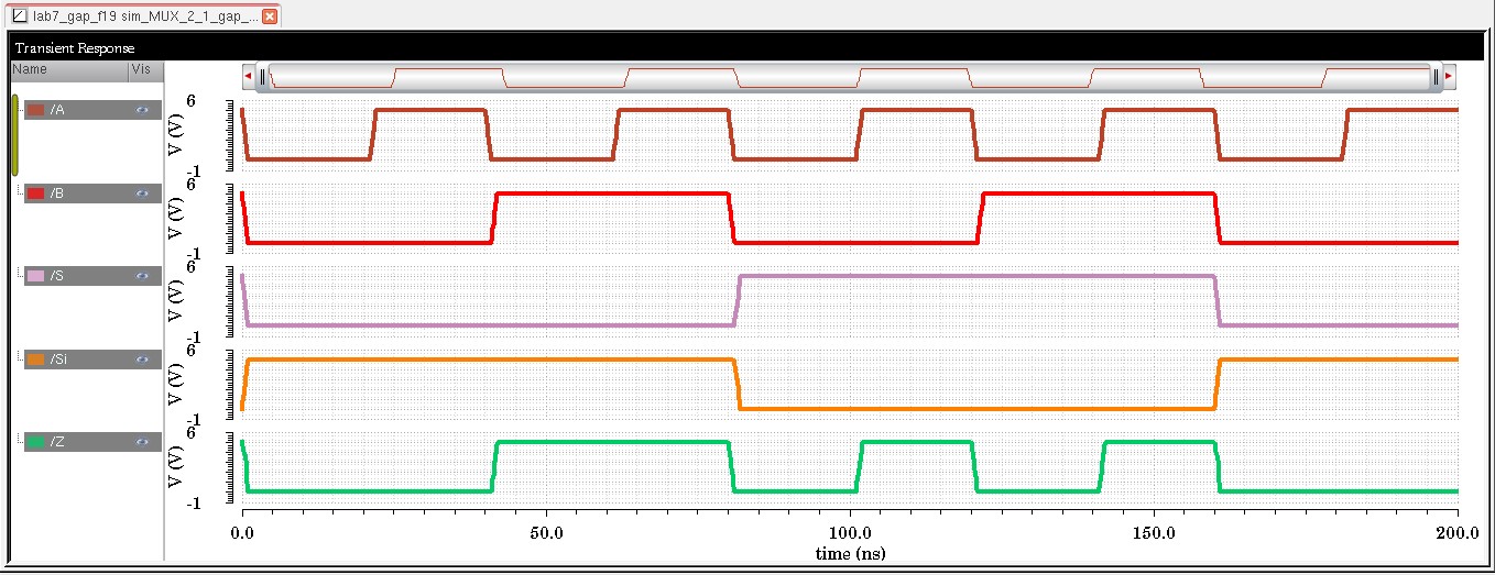
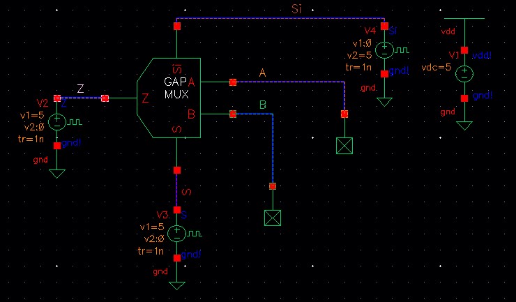
Next examine the schematic of a 2-to-1 DEMUX/MUX (and the symbol).
Simulate the operation of this circuit using Spectre and explain how it works.
| MUX/DEMUX | |
| Schematic | Symbol |
 |  |
| MUX Simulation Schematic | Plot |
 |  |
| DEMUX Simulation Schematic | Plot |
 |  |
As seen in the MUX plot, when S is set to '0', the output becomes that of the B input and when S is set to '1' the output is becomes that of the A input.
And in the DEMUX plot we see that when S is '1' B takes the signal of Z, though A remains '1' at this time. Then when S is '0', A takes the signal ofZ.
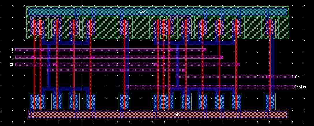
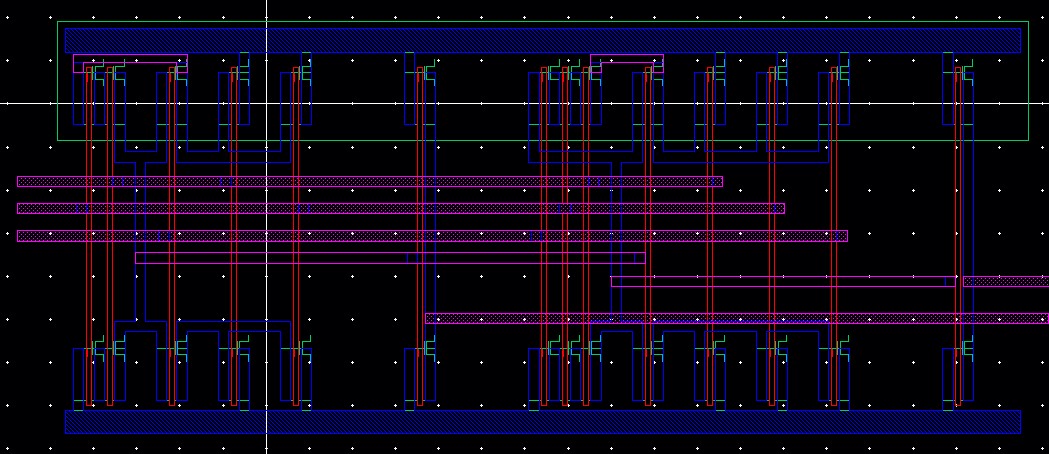
| 8-bit MUX/DEMUX | |
| Schematic | Symbol |
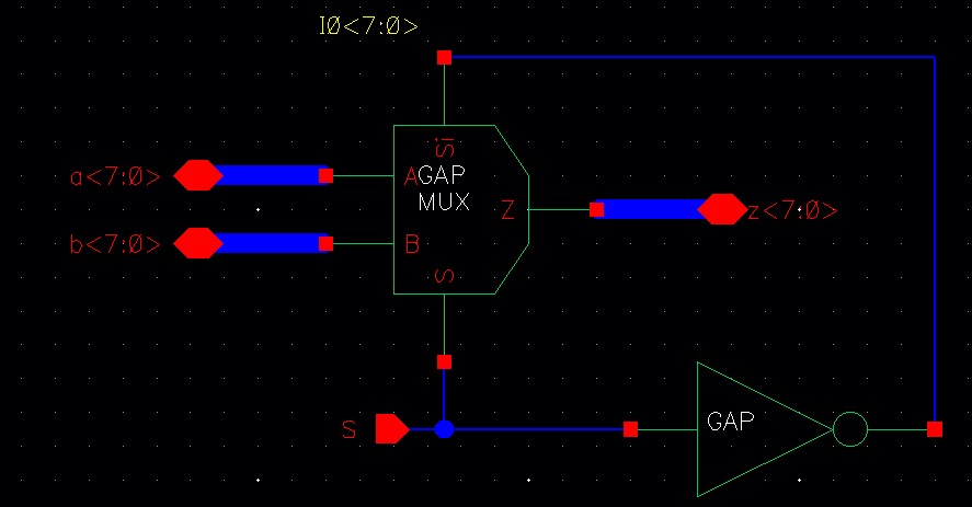 | 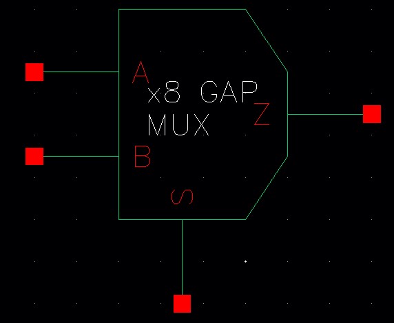 |
| Simulation | |
| Schematic | Plot |
 | 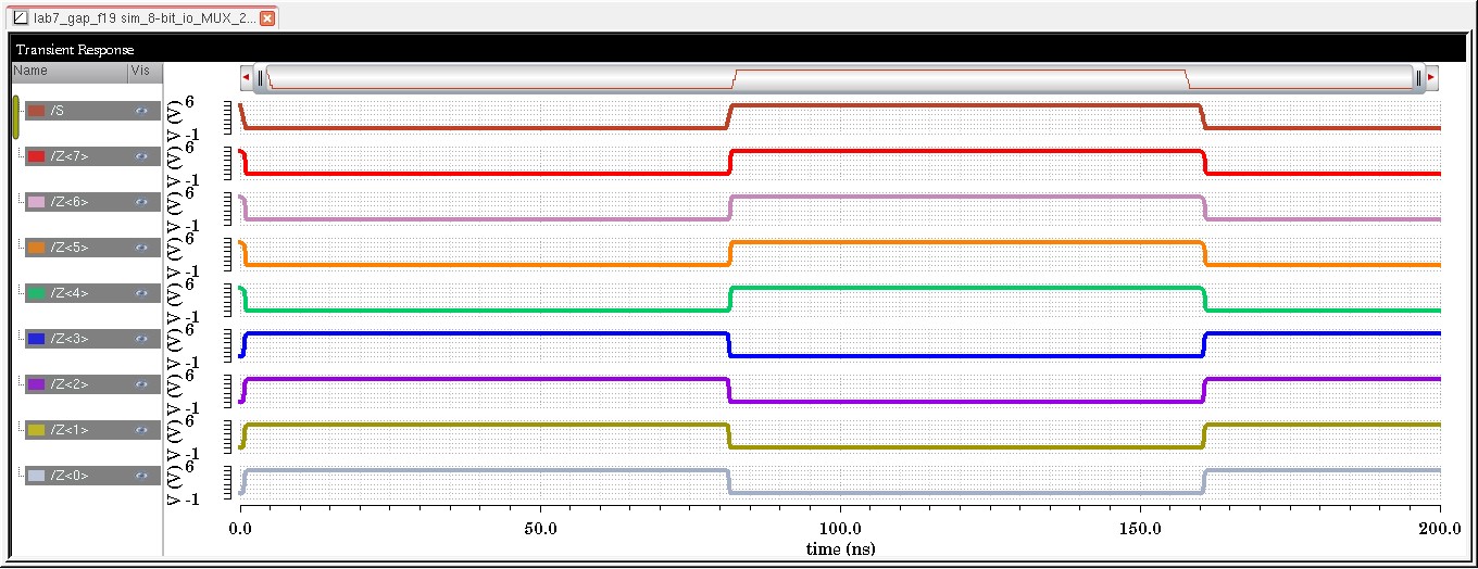 |
| Full-adder | |
| Schematic | Symbol |
 |  |
| Layout | Extraction |
 |  |
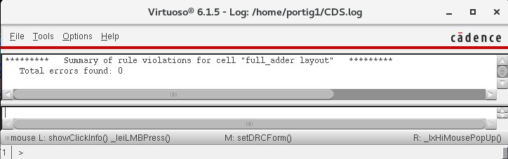
| DRC | LVS |
 |  |
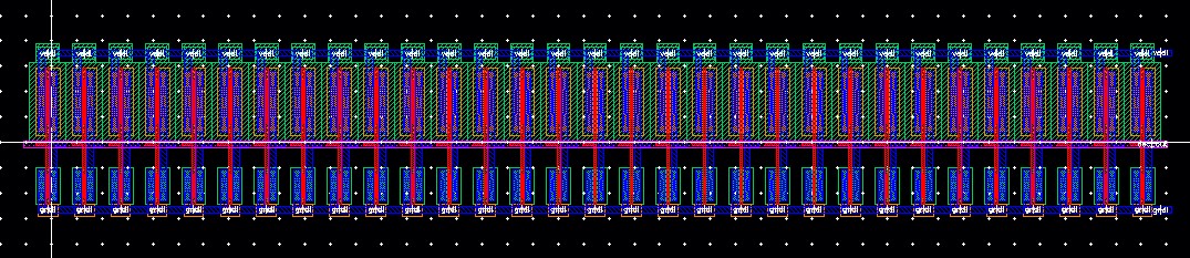
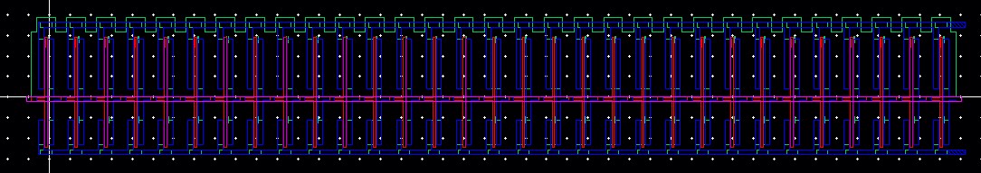
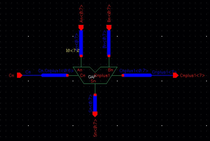
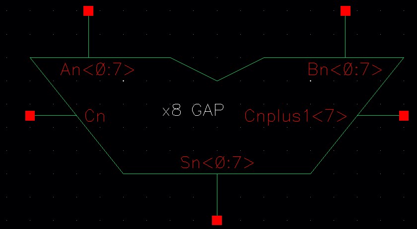
| 8-bit Full-Adder | |
| Schematic | Symbol |
 |  |
| Layout | Extraction |
 |  |
| DRC | LVS |
 |  |
| Schematic | Plot |
 |  |
In the above schematic, when A or B are high or low they will have an 8-bit value such as '1111 1111' and '0000 0000', When Cn is high, we can see that the sum (Sn<0:7>) is '0000 0001'. And when A or B are high and nothing else, the sum is '1111 1111'. Then when A and Cn are high or B and Cn are high, the sum is then
'0000 0000' and Cout(Cnplus1<7>) is '1'. When A and B are high but not Cn, the sum is '1111 1110' and Cout is '1'. When A, B and Cn are high, the sum is '1111 1111' and Cout is '1'.
End of lab Backup