 Lab 8 – EE 421L
Authored by:
Daniel Senda, Brian Kiaer, Victor Martinez
Fall 2018
Due: 12-05-2018
1) Pre-Lab Description
-The
first task was to back-up all of the previous work from the previous labs. The
second task was to go through and finish tutorial 6.
- Tutorial
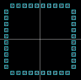
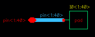
6 goes over the design and layout of padframe
for fabrication, as well as the process of placing circuit layouts in padframe. The following are a few images showing the
completion of tutorial 6.
Pad layout: Pad
schematic: ↓
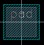

Padframe layout: Padframe schematic: ↓
2) Description of Lab
Procedures
- The first task of the lab was to form a group
of three students. This group is composed of Brian Kiaer,
Victor Martinez, and Daniel Senda. As a group, circuits will
be placed on a chip and will be tested once manufactured.
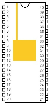
- Each test
circuit must have its own power but ground (Pin 20) can be
shared between all the circuits that will be laid out on the chip.
- The chip
will include the following:
·
One
or more course projects.
·
A
31-staged ring oscillator with a buffer for diving a 20pF off-chip load.
·
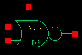
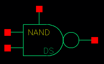
NAND
and NOR gates using 6/0.6u NMOSs and PMOSs
·
An
inverter made with a 6/0.6u NMOS and a 12/0.6u PMOS
·
Transistors,
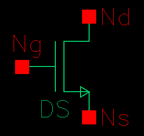
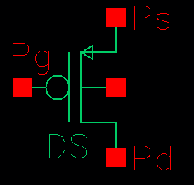
both PMOS and NMOS, measuring 6u/0.6u where all 4 terminals of each device are connected to bond pands.
·
Using
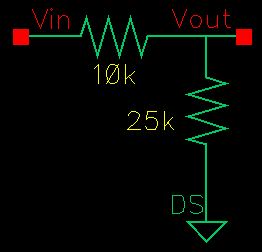
the 25k resistor and a 10k resistor implement a voltage divider.
·
A
25k resistor implemened using the n-well
- The following
table shows what each pin the chip is designated for:
|
Pin<1:20> |
Labels |
Diagram |
Labels |
Pin<21:40> |
|
Pin 1 |
N/A |
|
Vdd5 |
Pin 21 |
|
Pin
2 |
NOR Out |
VFB1 |
Pin
22 |
|
|
Pin
3 |
Vdd1 |
Vout1 |
Pin
23 |
|
|
Pin
4 |
NAND Out |
Vdd6 |
Pin
24 |
|
|
Pin
5 |
Vdd2 |
VFB2 |
Pin
25 |
|
|
Pin
6 |
Input A |
Vout2 |
Pin
26 |
|
|
Pin
7 |
Input B |
Osc. Out |
Pin
27 |
|
|
Pin
8 |
Inv. Out |
Vdd7 |
Pin
28 |
|
|
Pin
9 |
Vdd3 |
Vdd8 |
Pin
29 |
|
|
Pin
10 |
Inv. In |
Din |
Pin
30 |
|
|
Pin
11 |
N Drain |
Clk_in |
Pin
31 |
|
|
Pin
12 |
N Gate |
D7 |
Pin
32 |
|
|
Pin
13 |
N Source |
D6 |
Pin
33 |
|
|
Pin
14 |
P Drain |
D5 |
Pin
34 |
|
|
Pin
15 |
P Gate |
D4 |
Pin
35 |
|
|
Pin
16 |
P Source |
D3 |
Pin
36 |
|
|
Pin
17 |
Vdd4 |
D2 |
Pin
37 |
|
|
Pin
18 |
Vin V-divider |
D1 |
Pin
38 |
|
|
Pin
19 |
Vout V-divider |
D0 |
Pin
39 |
|
|
Pin
20 |
GND |
Clk_out |
Pin
40 |
- After
getting designating pins to the appropriate circuit pins, the schematic and
layout were created.
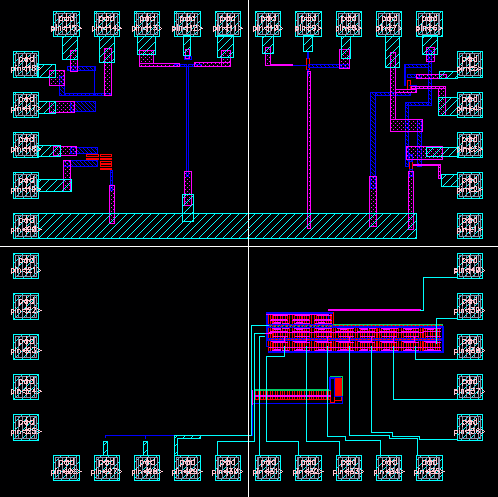
Chip design schematic:
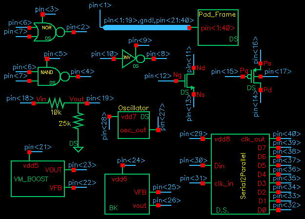
Chip design layout:
- After
completing the schematic and layout, the student created a guide to test the
circuits put on the chip:
NOR gate:
NAND gate:
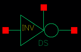
Inverter:
NMOS:
PMOS:
Voltage
divider:
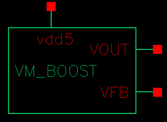
Victor’s
boost SPS:
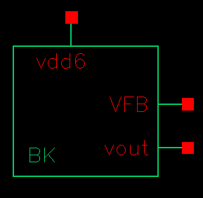
Brian’s
boost SPS:
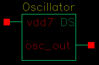
Oscillator:
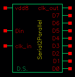
Daniel’s
Serial-to-parallel converter:
The files
for this lab can be found in the following link: lab8.zip
This concludes lab 8.
Additional Links
→ Return to listing of
lab reports
→ Daniel’s CMOS
homepage
→
Dr. Baker’s CMOS homepage