 Lab 7 – EE 421L
Authored by: Daniel Senda
Email: sendad1@unlv.nevada.edu
Fall 2018
Due: 11-07-2018
1) Pre-Lab Description
-The first
task was to back-up all of the previous work from the previous labs. The second
task was to go through and finish tutorial 5.
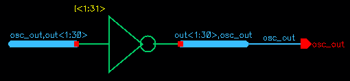
- Tutorial
5 goes over the design, layout, and simulation of a ring oscillator. The
following are a few images showing the completion of tutorial 5.
Ring oscillator schematic view:
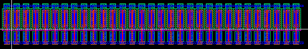
Layout View:
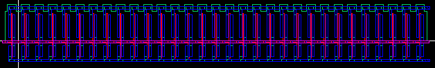
Extracted View:
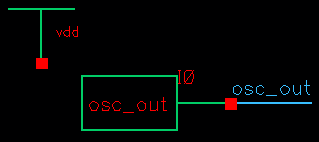
Ring oscillator symbol and simulation
schematic:
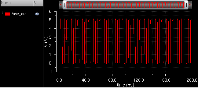
Ring oscillator simulation results:
2) Description of Lab
Procedures
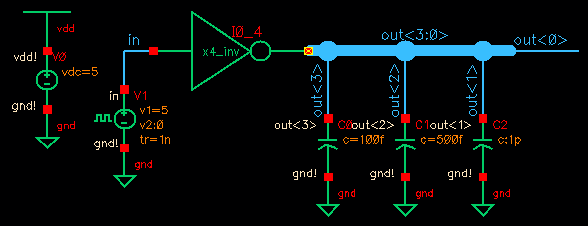
-The first
procedure in this lab had the student create a more concise schematic for an
existing circuit of 4 inverters. The student had to
make use of wide wires (buses), instance array names, and pin array names.
4 inverter circuit:
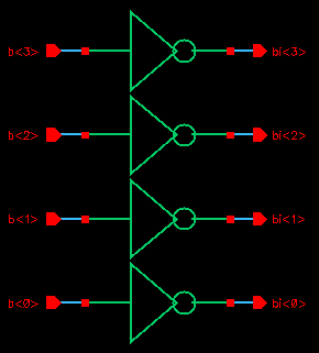
Concise 4 inverter
schematic: 4 Inverter symbol:
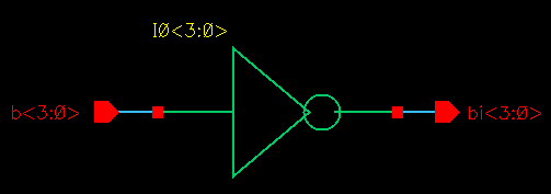
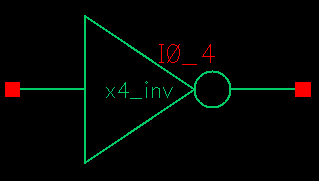
The inverter in the concise schematic was named using arrayed names seen above.
-After the 4 inverter symbol was created, the student was required to create
a simulation schematic to confirm proper operation of the 4 inverters using
different loads per inverter.
Simulation schematic:
Simulation waveform results:
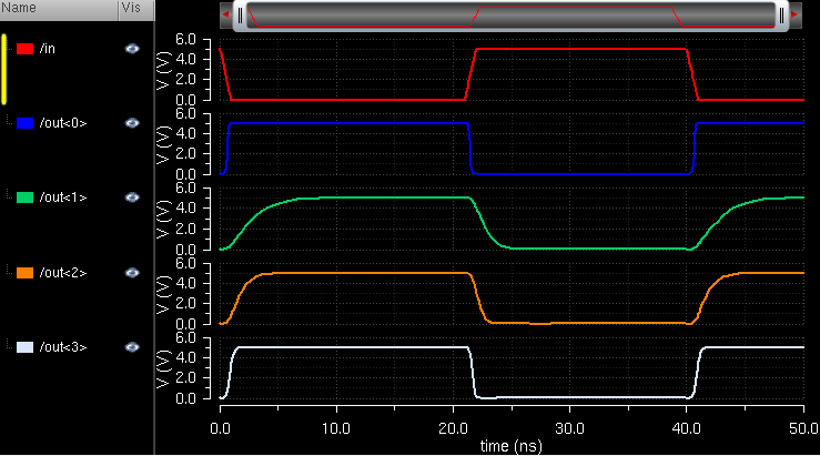
As can be seen in the waveform, the inverters with larger capacitive loads have
have longer rise times. The inverter that did not have any external capacitive
load (out<0>) has a relatively sharp rise and fall time compared to the
inverter that has the largest load(out<1>).
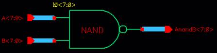
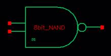
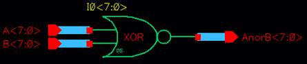
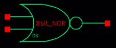
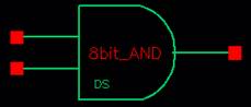
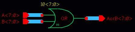
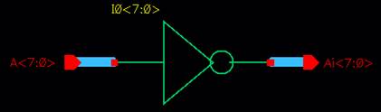
-The student
then created schematics and symbols for 8-bit input/output arrays of the
following gates: NAND, NOR, AND, OR, and inverter. Simulations are further down
below to demonstrate proper operation of gates.
8-bit NAND
gate array:
Schematic: Symbol:
8-bit NOR gate
array:
Schematic: Symbol:
8-bit AND
gate array:
Schematic: Symbol:

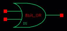
8-bit OR
gate array:
Schematic: Symbol:
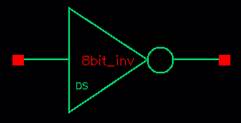
8-bit
inverter gate array:
Schematic: Symbol:
After
finishing the 8-bit gate arrays, the student created a simulation schematic to
test out the 8-bit gate arrays.
Schematic for gate simulations:
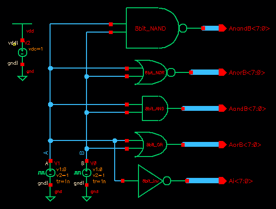
Gate simulation waveforms:
The inputs are A and B. The outputs displayed are of the first gate in each
8-bit array (gate<0>).
-The next
part of the lab required the student to understand and simulate the operation
of a 2-to-1 DEMUX/MUX.
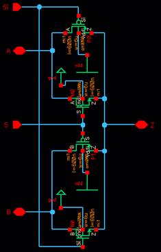
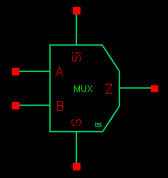
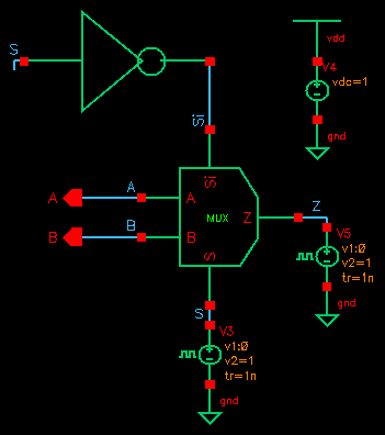
DEMUX/MUX schematic: DEMUX/MUX symbol:
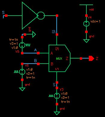
The
following schematic was used to simulate the MUX:
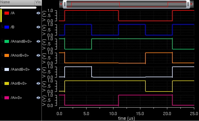
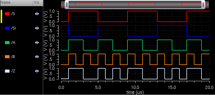
A MUX can be described like a type of switch. A 2-to-1 MUX
contains 2 inputs (A and B), 1 output (Z), and 2
selector inputs (S, Si). Si should always be the inverted signal of S, so for
explanation purposes, only the value of S will be considered. The selector input,
S, controls which input is connected to output Z. When
S goes high, input A is selected and gets connected to
the output Z. When S goes low, input B is selected and
is connected to the output Z
The simulation below shows the working operation of the MUX. (Si can be ignored)
2-to-1 MUX simulation waveform:
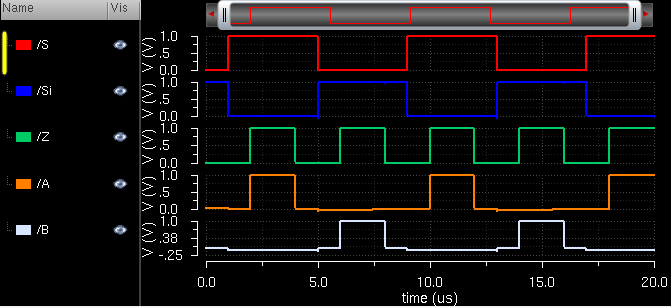
The
following schematic was used to simulate the DEMUX:
A DEMUX can also be described like a type of switch. A 1-to-2 DEMUX
contains 1 input (Z), 2 outputs (A and B), and 2
selector inputs (S, Si). Again, Si should always be the inverted signal of S,
so for explanation purposes only the value of S will be
considered. The selector input, S, controls which output gets connected to input Z. When S goes high, output A is
selected and gets connected to input Z. When S goes
low, output B is selected and is connected to input Z.
The simulation below shows the working operation of the DEMUX. (Si can be
ignored)
1-to-2 DEMUX simulation waveform:
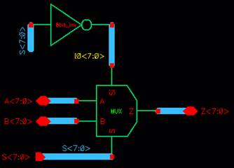
-The next step after simulating the DEMUX/MUX, the student created a schematic and symbol for an
8-bit input/output array of the DEMUX/MUX.
The symbol was simulated to demonstrate proper
operation of the design.
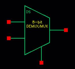
8-bit
DEMUX/MUX array schematic: Symbol:
The student
created a simulation schematic to test out the 8-bit DEMUX/MUX symbol.
Schematic DEMUX/MUX simulation:
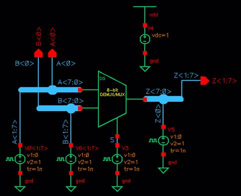
DEMUX/MUX simulation waveforms:
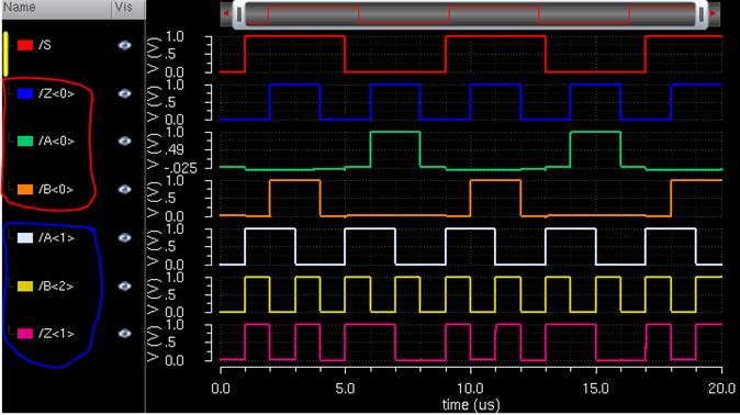
All 8-bits of the symbol share the same selector signal (S). The I/O signals circled
in red are from the 1st bit which was used
as a DEMUX; the outputs (A and B) show proper operation. The I/O signals
circled in blue are from the 2nd bit which
was used as a MUX; the output (Z) shows proper operation. The rest of the bits
are also used as MUXes identical to the 2nd bit.
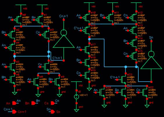
-Following
the lab 7 guidelines, the student drafted the schematic of a full-adder using
6u/0.6u devices (both PMOS and NMOS) and also created
a symbol for it.
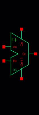
Full-adder schematic: Symbol:
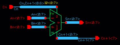
-Then
student then created an 8-bit full adder schematic and symbol. In addition, a
simulation schematic was created to show correct
operation of the 8-bit adder.
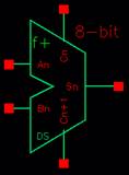
8-bit full-adder
array schematic: Symbol:
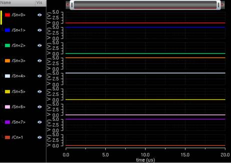
Two numbers were selected to test the 8-bit full adder as follows. No
carry-in was used.
1st number (An) – 01111111 (127)
2nd number (Bn) – 00011011 (27)
Total sum (Sn) – 10011010 (154)
8-bit full adder simulation
schematic:
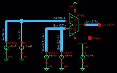
Simulation waveform results:
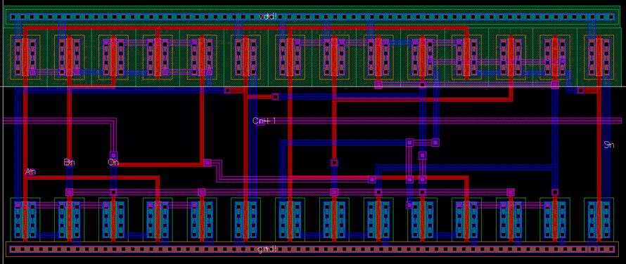
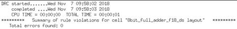
-In the last
section of the lab, the student created the layout for the 8-bit full adder.
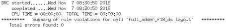
The student also did DRC and LVS checks to make sure the layout was correct.
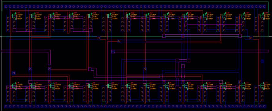
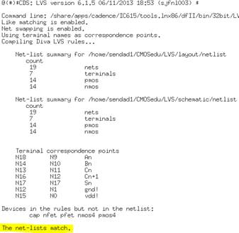
The first
step to create the 8-bit adder was to create a single adder first, as shown
below.
Full-adder layout view:
DRC Results: Shows no errors.
Full-adder extracted view:
Full-adder LVS results: Shows that
the netlist match.
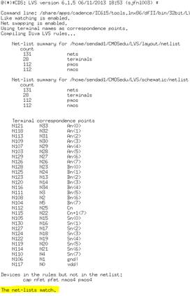
The last
procedure was to create the layout of the 8-bit full adder using the single
adder layout.
8-bit full-adder schematic view:

DRC Results: Shows no errors.
8-bit full-adder extracted view:

8-bit full-adder LVS results: Shows
that the netlist match.
All of the
files for this lab can be found in the following link: lab7_f18_ds.zip
This
concludes lab 7.
Additional Links
→ Return to listing of
lab reports
→ Daniel’s CMOS
homepage
→
Dr. Baker’s CMOS homepage