 Lab 6 – EE 421L
Authored by: Daniel Senda
Email: sendad1@unlv.nevada.edu
Fall 2018
Due: 10-24-2018
1) Pre-Lab Description
The first
task was to back-up all of the previous work from the
previous labs.
The second task
was to go through and finish tutorial 4.
- Tutorial
4 goes over the design, layout, and simulation of a CMOS NAND gate.
The following are a few images showing the completion of tutorial 4.
NAND Schematic View Layout View Extracted
View
Symbol View
2) Description of Lab
Procedures
The first
procedures of this lab had the student create schematics, layouts, and symbols for
a 2-input NAND gate and a 2-input XOR gate. The student was required to use
6u/0.6u MOSFETs (both NMOS and PMOS). The schematics and layouts also have to
pass the design rule check (DRC) and layout versus schematic (LVS) check.
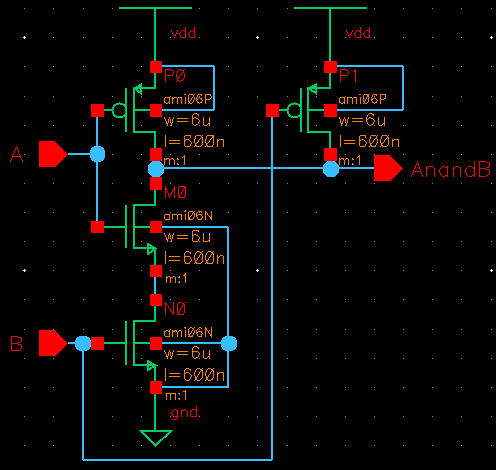
2-input NAND gate:
(Student was required to use a naming convention for the cells. Ex
“NAND2_ds_f18”)
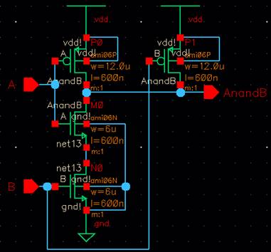
The following is the schematic layout of a 2-input NAND gate created through
MOSFTES.
Schematic view:
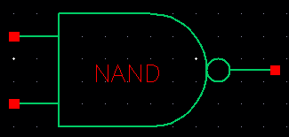
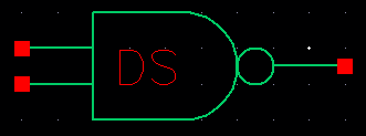
The symbol was created following the commonly used symbol for a NAND gate. The
student also added initials in the middle of the symbol as required.
Symbol view:
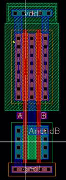
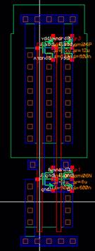
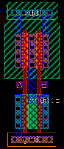
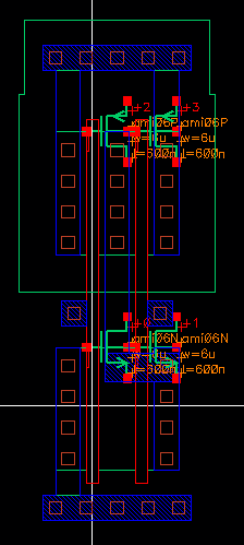
Next, the student created the layout of the NAND gate and then extracted it.
The student was required to route all of the inputs/outputs on the metal1 layer
as seen below.
Layout view: Extracted view:
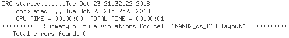
Before the layout was extracted in the last step, a DRC was ran and confirmed
that there were zero errors.
DRC results:
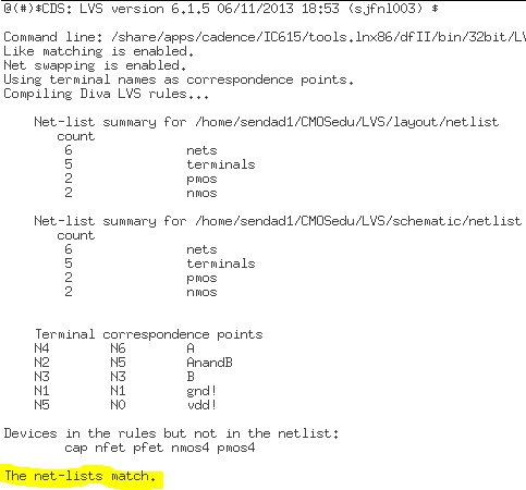
After the layout was extracted, a LVS check was ran and confirmed that the
layout matched the schematic.
LVS results:
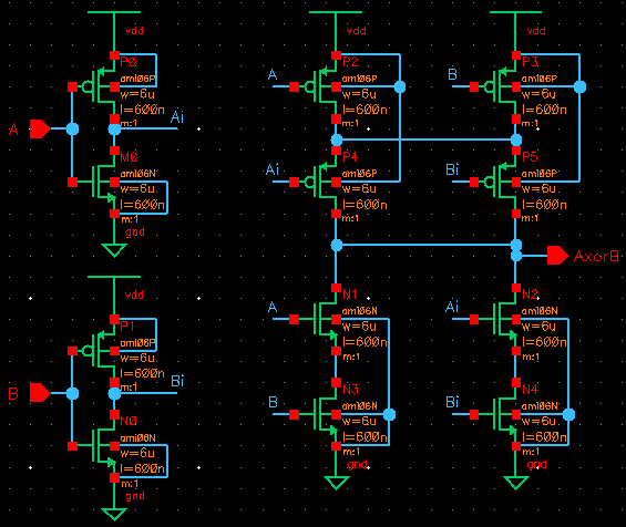
2-input XOR gate:
The following is the schematic layout of a 2-input XOR gate created through
MOSFTES.
Schematic view:
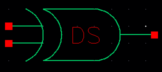
The symbol was created following the commonly used symbol for an XOR gate.
Again, the student added initials in the middle of the symbol as required.
Symbol view:
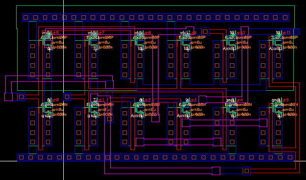
Next, the student created the layout of the XOR gate and then extracted it as
seen below.
Layout view:
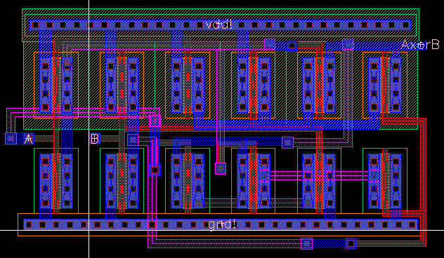
Extracted view:
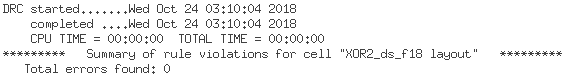
Before the layout was extracted in the previous step, a DRC was ran and
confirmed that there were zero errors.
DRC results:
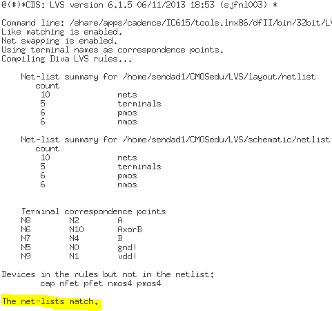
After the layout was extracted, a LVS check was ran and confirmed that the
layout matched the schematic.
LVS results:
Simulations:
NAND Gate
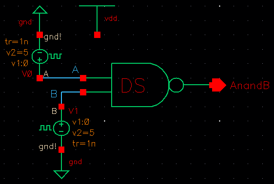
The following is the schematic that was used to test the NAND gate.
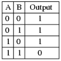
Schematic view and NAND truth table:
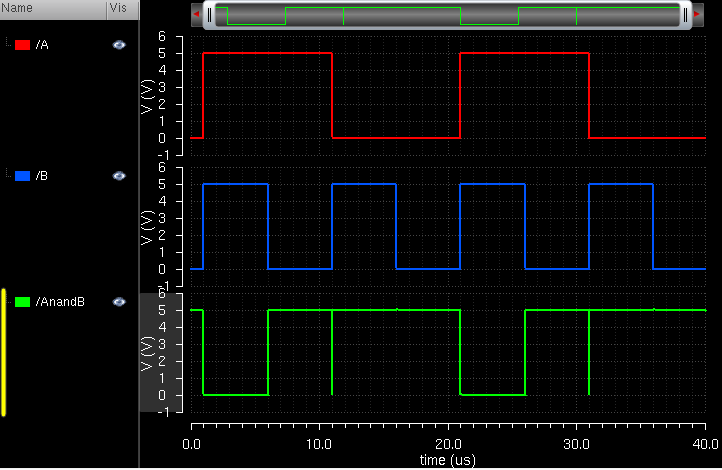
The following
graph proves that the NAND gate works as intended. The output has a little glitch
when both inputs transition at the same time because of the timing, but it
promptly goes back to normal.
Simulation waveform results:
XOR Gate
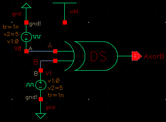
The following is the schematic that was used to test the XOR gate.
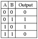
Schematic view and XOR truth table:
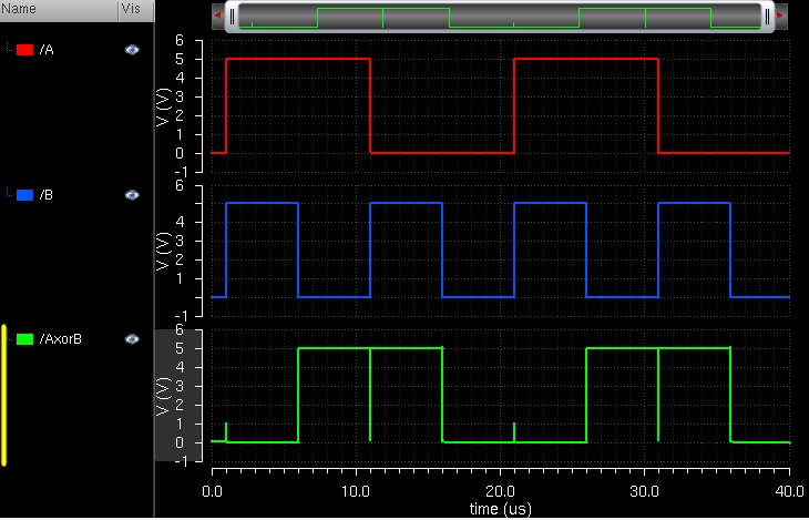
The following
graph demonstrates that the XOR gate works as intended. Once again, the output
has a glitch when both inputs transition at the same time, but it quickly goes
back to normal.
Simulation waveform results:
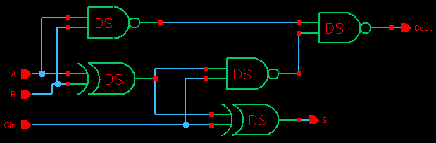
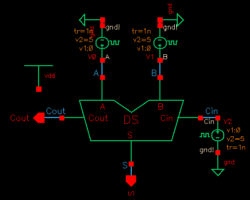
Full Adder:
The last part of the lab had the student create a schematic, symbol, simulation,
and layout of a full adder.
Schematic view of full adder:
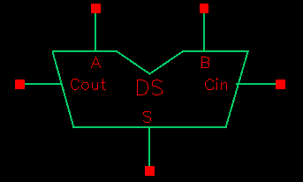
Symbol view of full adder:
To test
operation of the full adder, a simulation schematic was made.
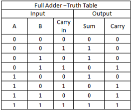
Simulation schematic and full adder truth
table:
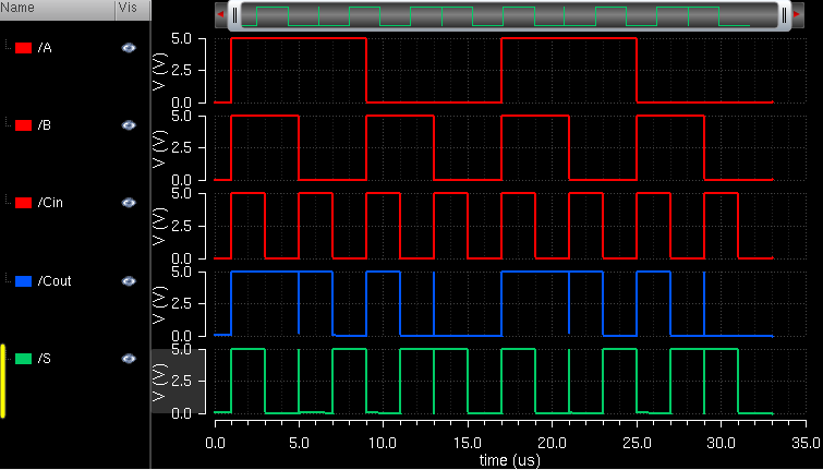
A simulation
was then ran, and the following results confirm proper
operation of full adder.
Simulation waveform results:
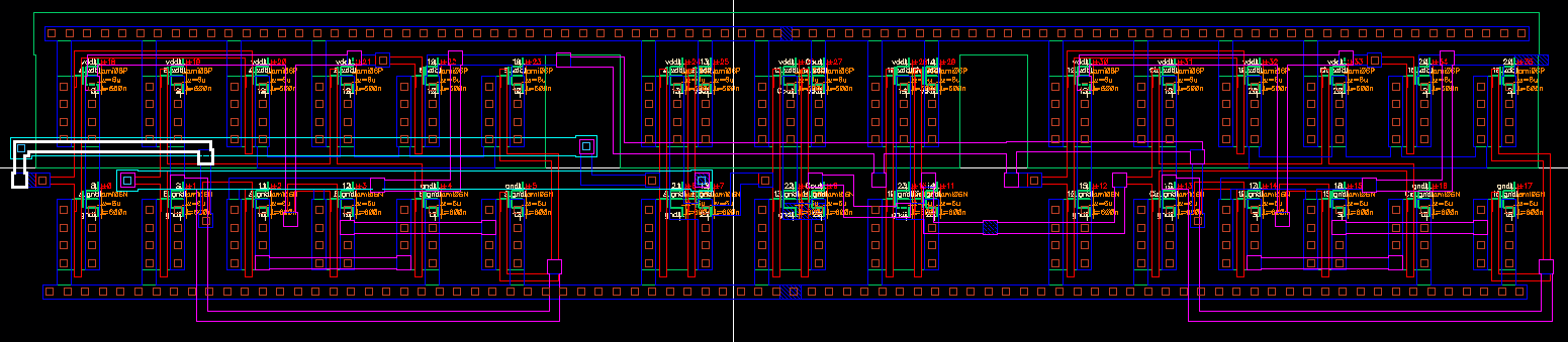
Layout view of full adder:
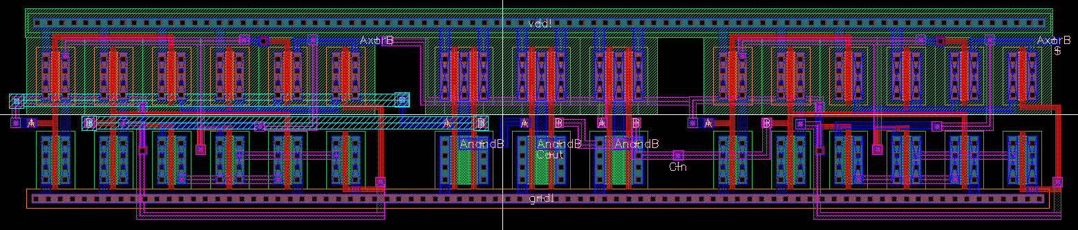
Extracted
view of full adder:
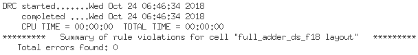
Before the
layout was extracted in the previous step, a DRC was ran
and confirmed that there were zero errors.
DRC results:
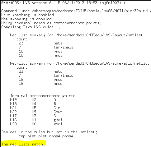
After the
layout was extracted, a LVS check was ran and
confirmed that the layout matched the schematic.
LVS results:
All of the
files for this lab can be downloaded in the following link: lab6.zip
This
concludes lab 6.
Additional Links
→ Return to listing of
lab reports
→ Daniel’s CMOS
homepage
→
Dr. Baker’s CMOS homepage