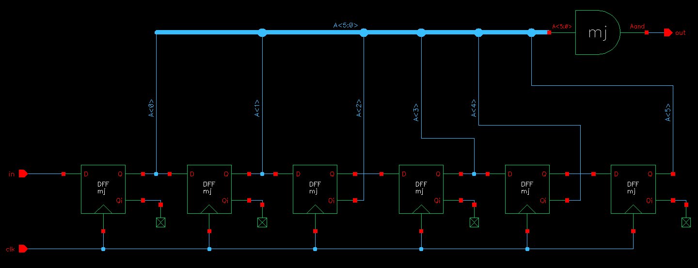
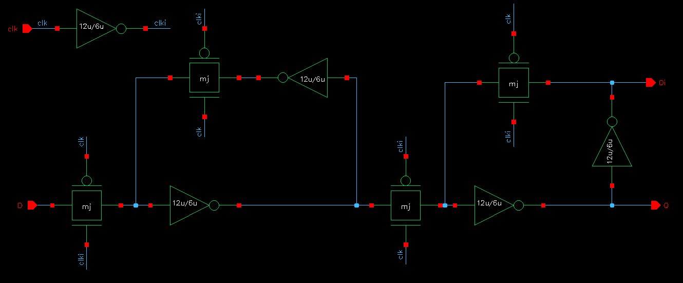
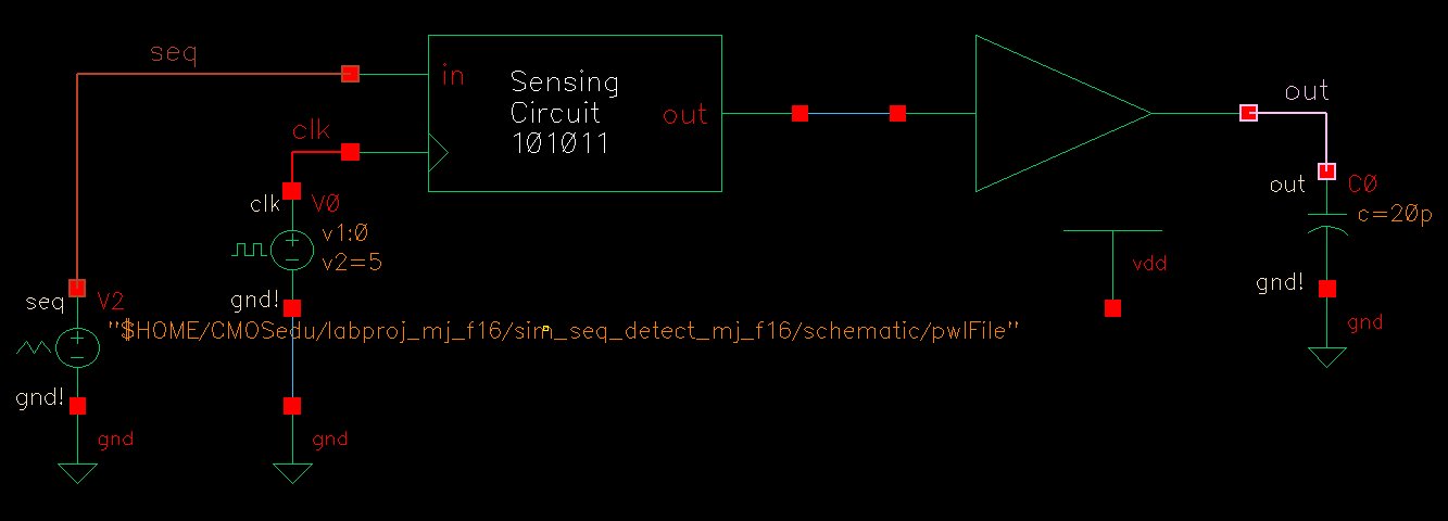
Schematic of sequence detector.
email: jaimem5 at the UNLV students domain
 |
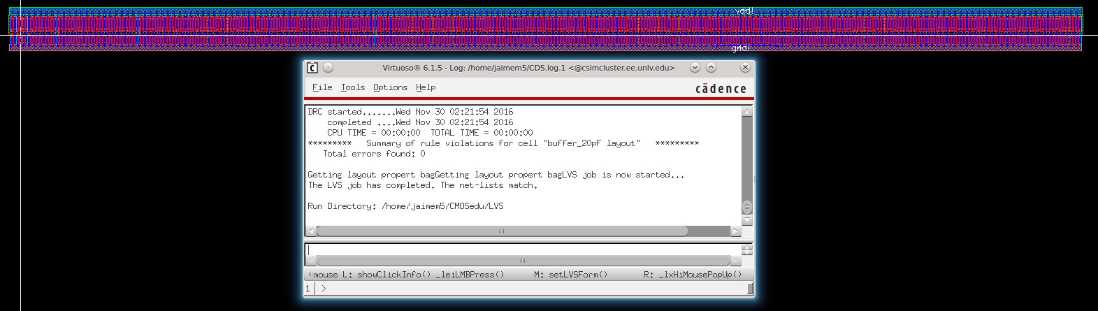
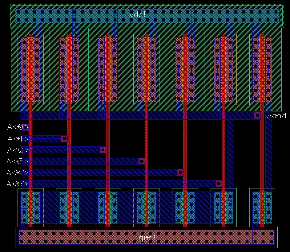
 A detailed image of the layout is found here.
|
 |
 |
 |
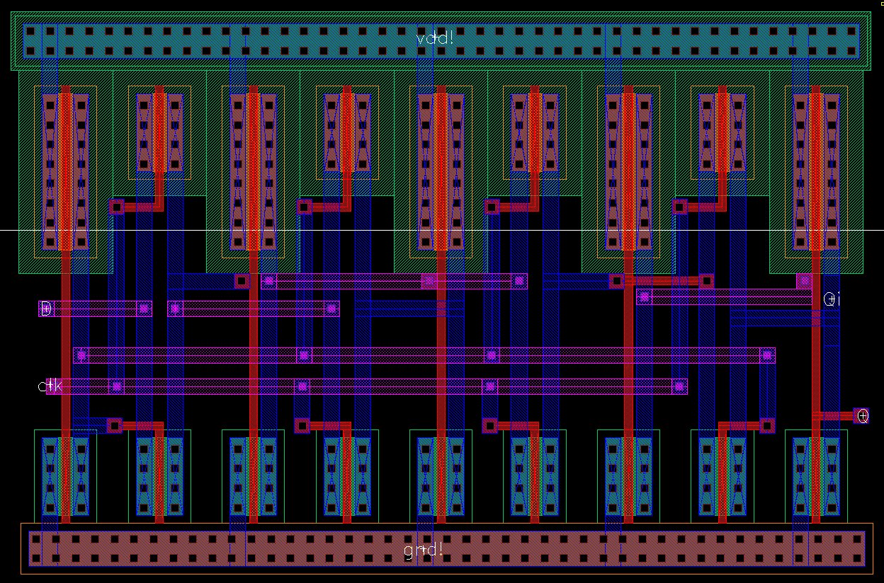
 A detailed image of the layout is found here.
|
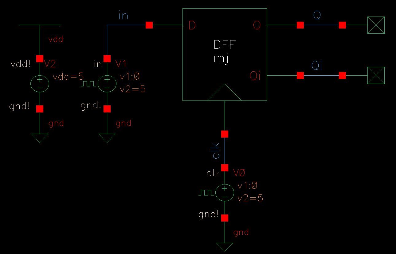 |
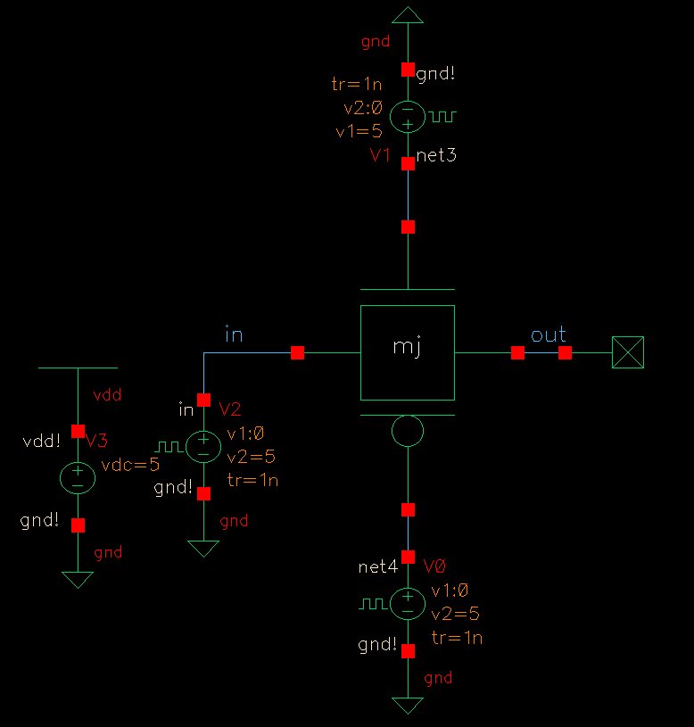
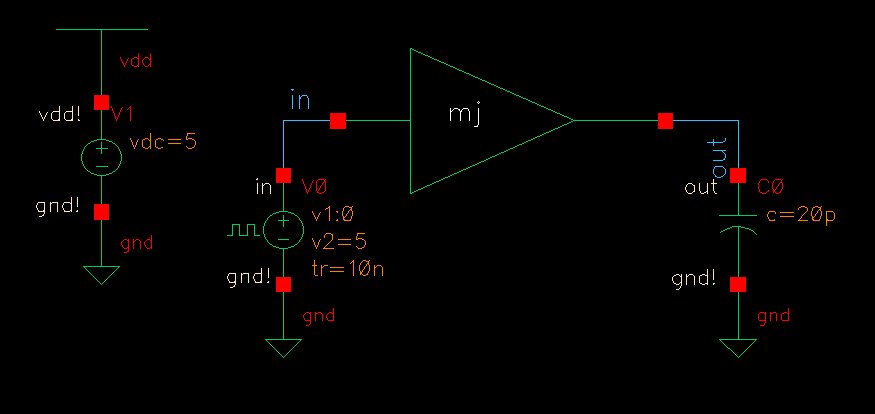
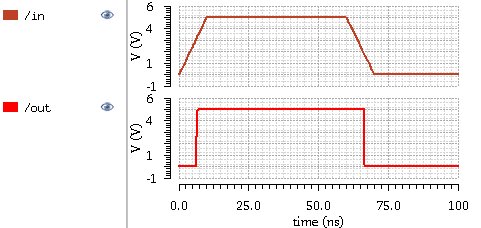
 The flip-flop reads in the input value at the rising edge of the clock. |
 |
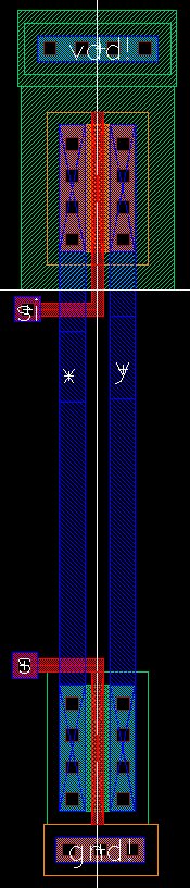
 A detailed image of the layout is found here. |
 |
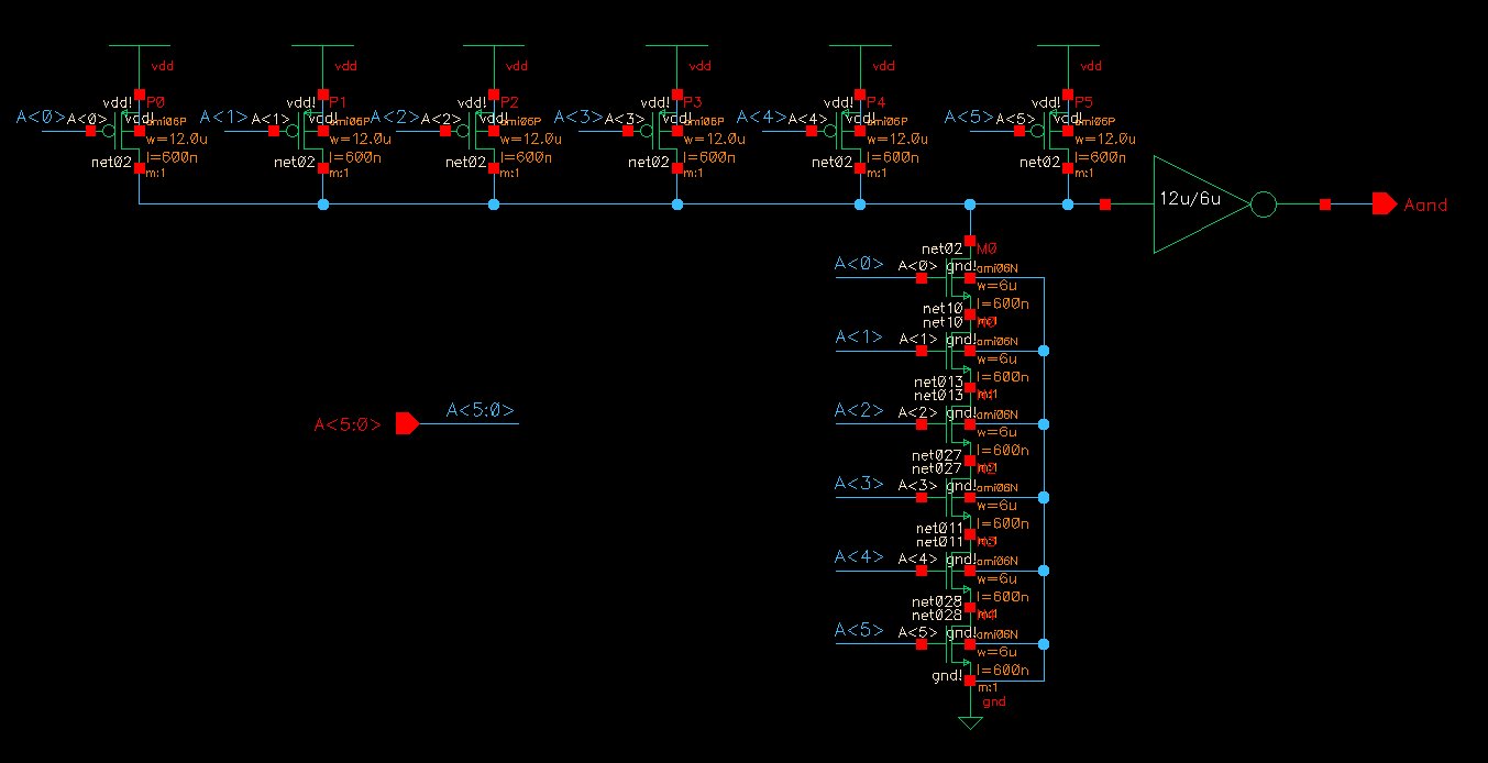
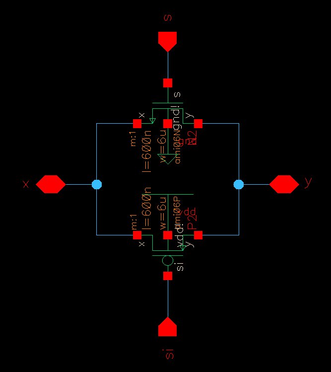
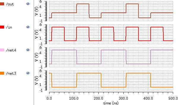 Note that the output of the gate only matches the input when the transistors are enabled on net3 and net4. |
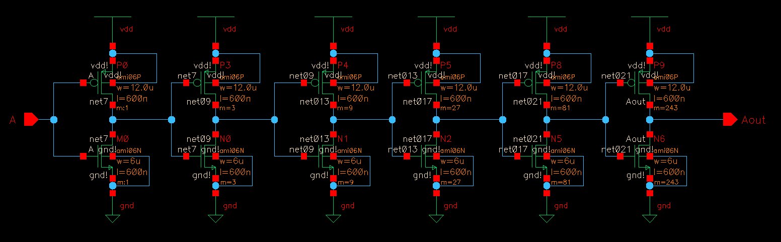 |
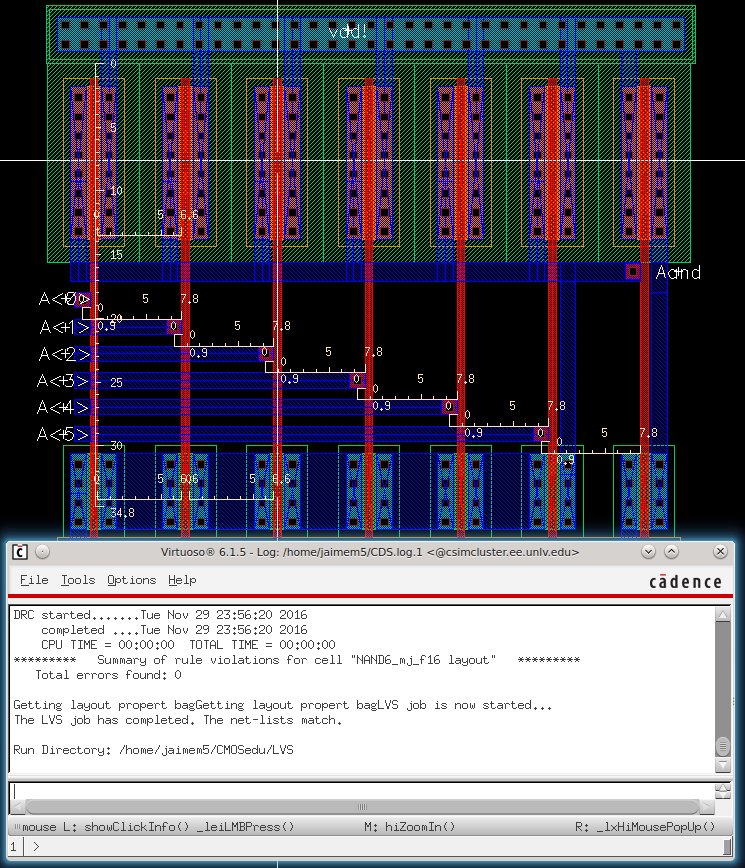
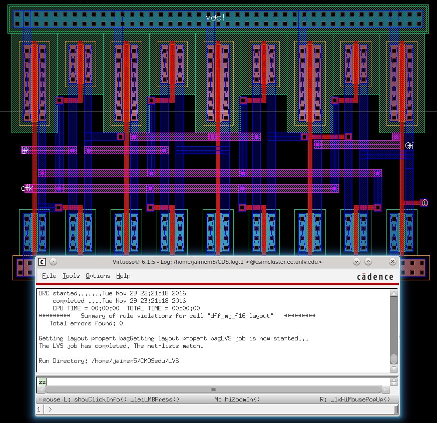
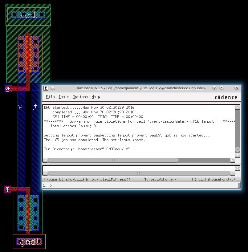
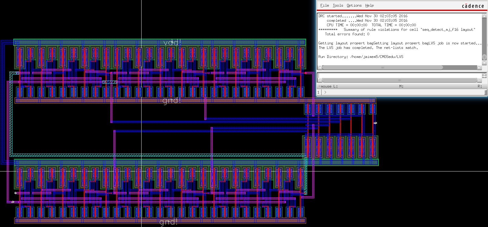
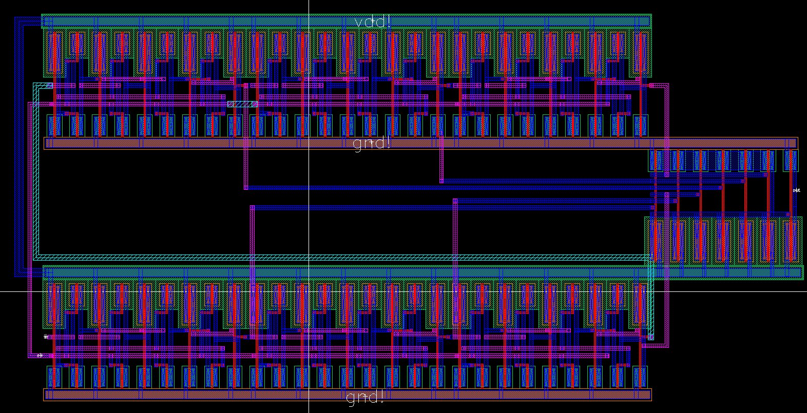
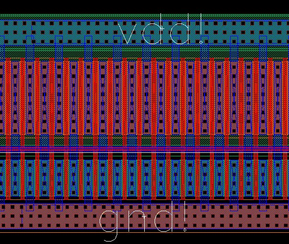
 The complete layout is difficult to see in an image, but here is a close up. |
  |
 |
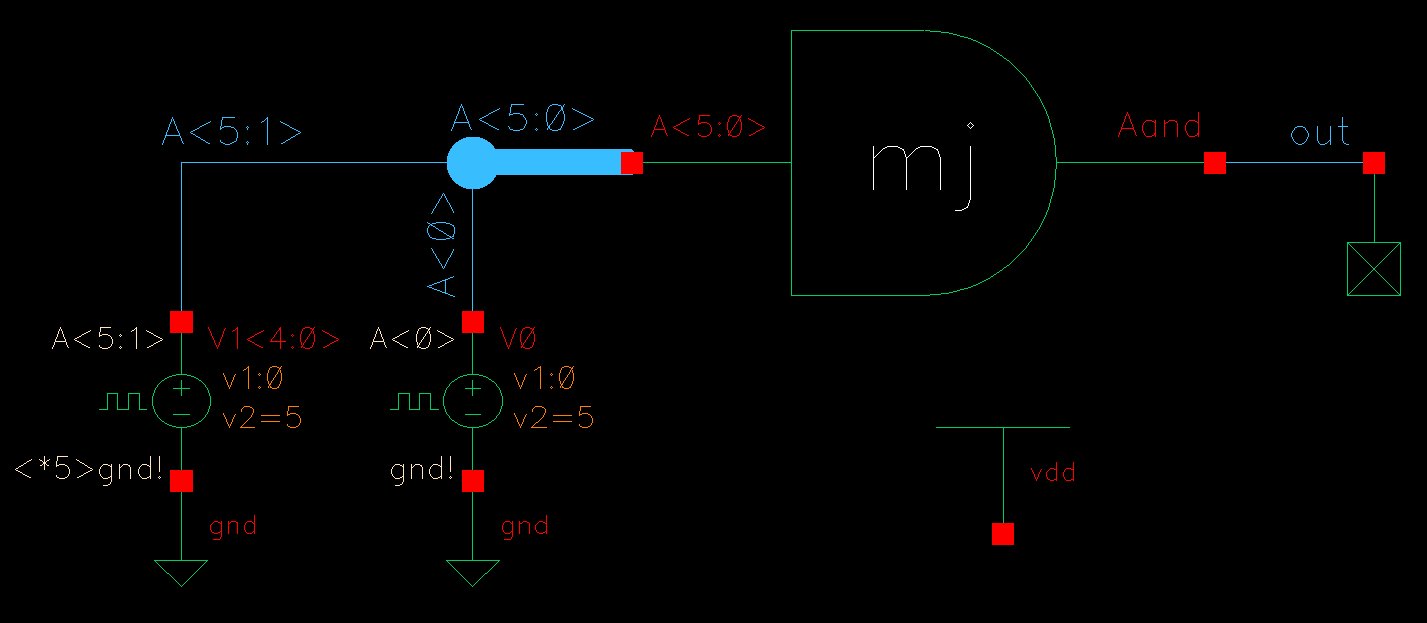
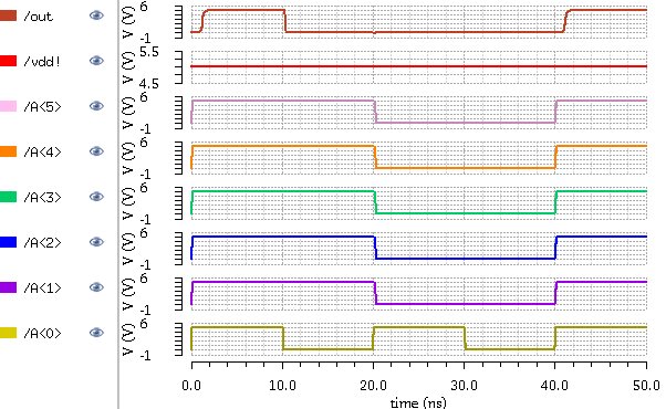
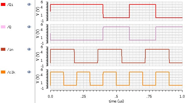
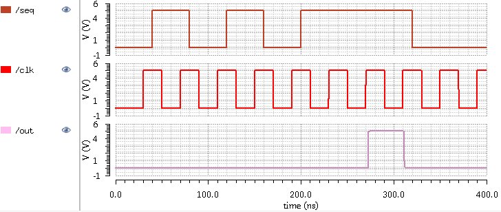 Input sequence: 0101011100. The output of the detecting circuit is only high when the register's value is 101011. |
 |
 |