Project - EE 421L
Authored
by Luis A. Soriano,
Email: sorian20@unlv.nevada.edu
Date: November 23, 2015
Project Description: Chip fabricated using the C5 process through MOSIS
Part 1: First half of the project includes schematics and simulations of the following circuits:
- Design of an 8-bit resettable (input "clear") up/down counter
- The outputs of your counter should be buffered before connecting to a pad
- A 31-stage ring oscillator with a buffer for driving a 20 pF off-chip load
- NAND and NOR gates using 6/0.6 NMOSs and PMOSs
- An inverter made with a 6/0.6 NMOS and a 12/0.6 PMOS
- Transistors,
both PMOS and NMOS, measuring 6u/0.6u where all 4 terminals of each
device are connected to bond pads (7 pads + common gnd pad)
- Note
that only one pad is need for the common gnd pad. This pad is used to
ground the p-substrate and provide ground to each test circuit
- A 25k resistor implemented using the n-well (connect between 2 pads but we also need a common gnd pad)
- Using the 25k resistor laid out above and a 10k resistor implement a
voltage divider (need only 1 more pad above the ones used for the 25k
resistor
All
schematic and symbols designed in this project have an extra vdd pin,
so each symbol will run indepedently with their own power source.
8-bit resettable up/down counter
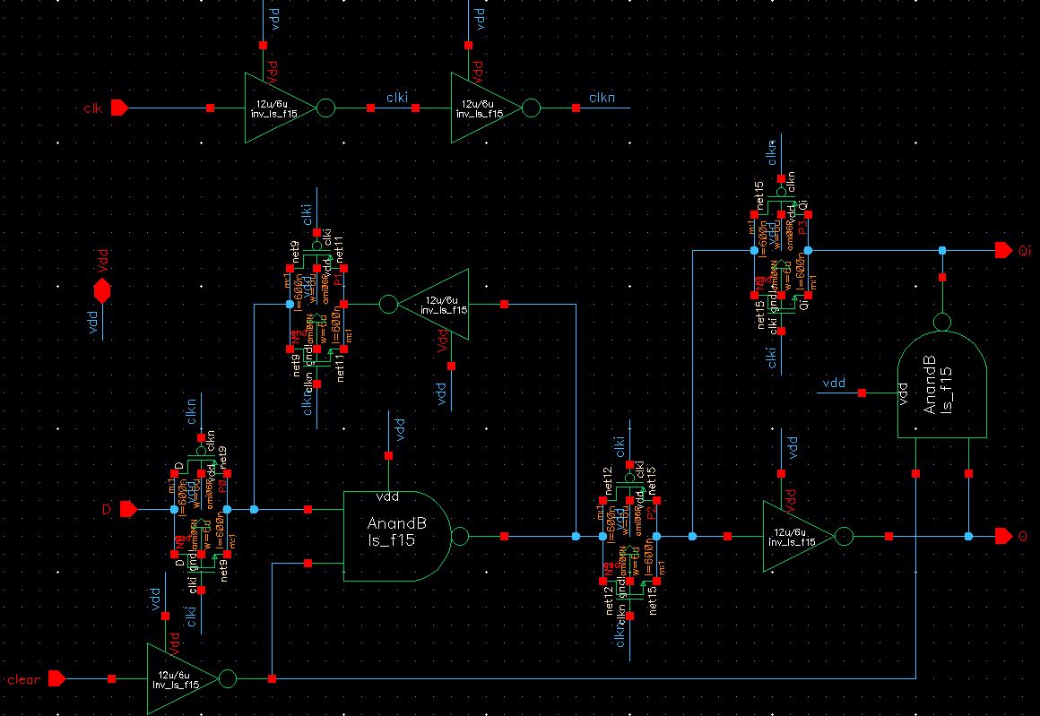
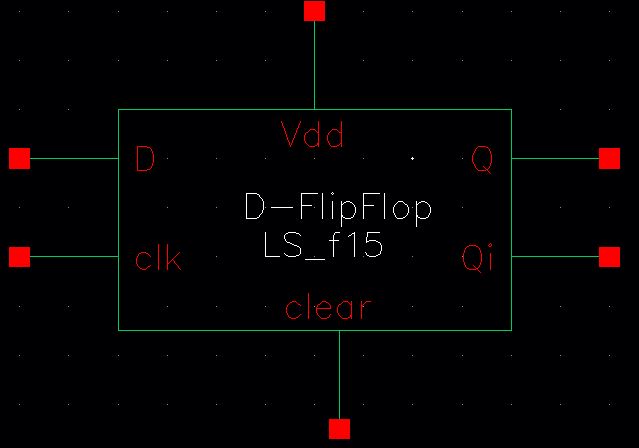
The main block used in the counter is the D-flip-flip with clear, whose schematic and symbol is shown below
| Schematic | Symbol |
 |  |
The
previous schematic was obtained based on the book. There are two latches
implemented in cascade. The first latch save the input D when the clock
goes down, and transfers it to the next stage when the clock goes high.
The clear input was implemented by replacing the two inverters with NAND
gates. Then, when clear is low, both NAND gates behaves as inverters.
When it's high, it sets Q output to zero no matter what value is stored
from the first latch. Also, the first latch output is set to zero, so
this values is passed when clear is set back to low. For the clock, two
inverters (buffer) were implemented for clock_bar and clock itslef to
avoid extra connections.
Truth table for D-flipflop is shown below.
| Clear | clk | D | Q |
| 0 | low-high | 0 | 0 |
| 0 | low-high | 1 | 1 |
| 0 | other | X | Q0 |
| 1 | X | X | 0 |
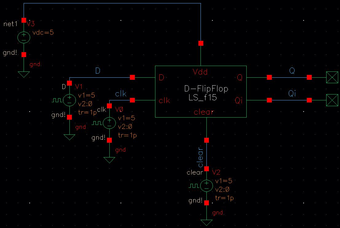
The following schematic is degined to simulate and verify the operation of the D-flip-flop
| Schematic | Simulation |
 | 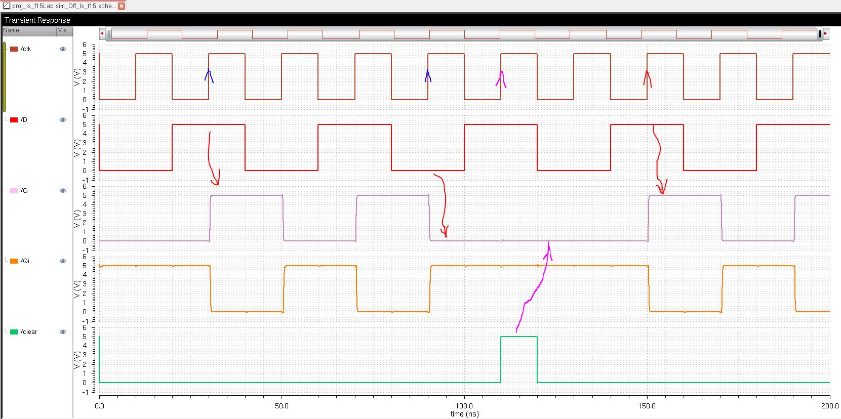 |
In
the above simulation, the D-flipflop operation is verified. It is seen
that, in clock rising edge, the current input value D is output in Q.
When 'clear' is high, the resulting output Q is set to zero, and Q_bar
to high (5v).
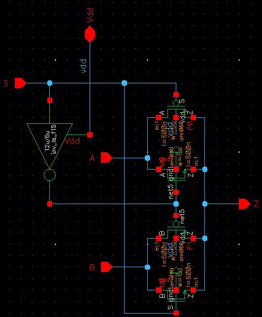
Furthermore, a 2-to-1 MUX is added to the counter to help us select either 'counting up' or 'counting down'.
| 2 to 1 MUX Schematic | Symbol |
 | 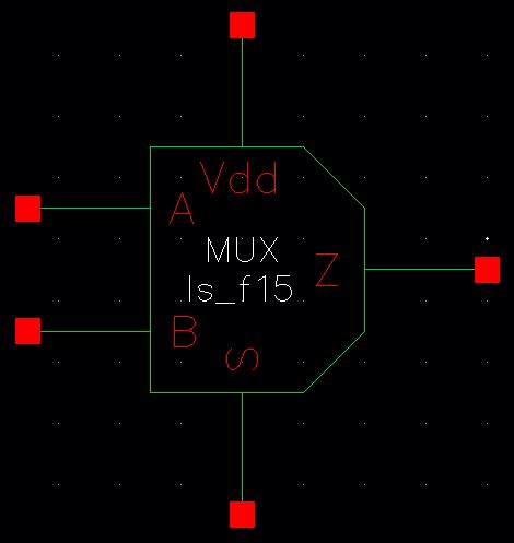 |
These two previous block are implemented in designing an 8 bit counter.
The
following table shows the operation of an up counter for 3 bits used as
a reference to be verified later through simulations.
| Q1 | 0 | 1 | 0 | 1 | 0 | 1 | 0 | 1 | 0 | 1 | |
| Q2 | 0 | 0 | 1 | 1 | 0 | 0 | 1 | 1 | 0 | 0 | and so on ... |
| Q3 | 0 | 0 | 0 | 0 | 1 | 1 | 1 | 1 | 0 | 0 | |
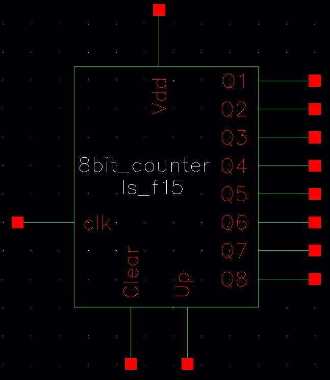
Next, the schematic of the 8-bit counter is shown below
| Schematic | Symbol |
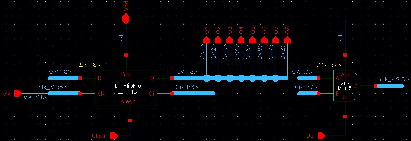 |  |
Either
output of the D-filpflop, Q and Q_bar, is connected to clock of the
next stage depending on counting down or up. When 'Up' is high, the
output Qi is connected to the clock of the next stage for counting up,
and when 'Up' is low, Q output is passed through the MUX to the next
stage for counting down. Arrays of buses have been used to implement
all conections through all 8 D-flipflops and 7 MUX's.
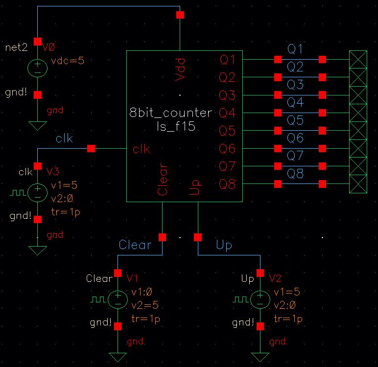
The operation of this counter is verified in the following schematic.
| Schematic | Simulation |
 | 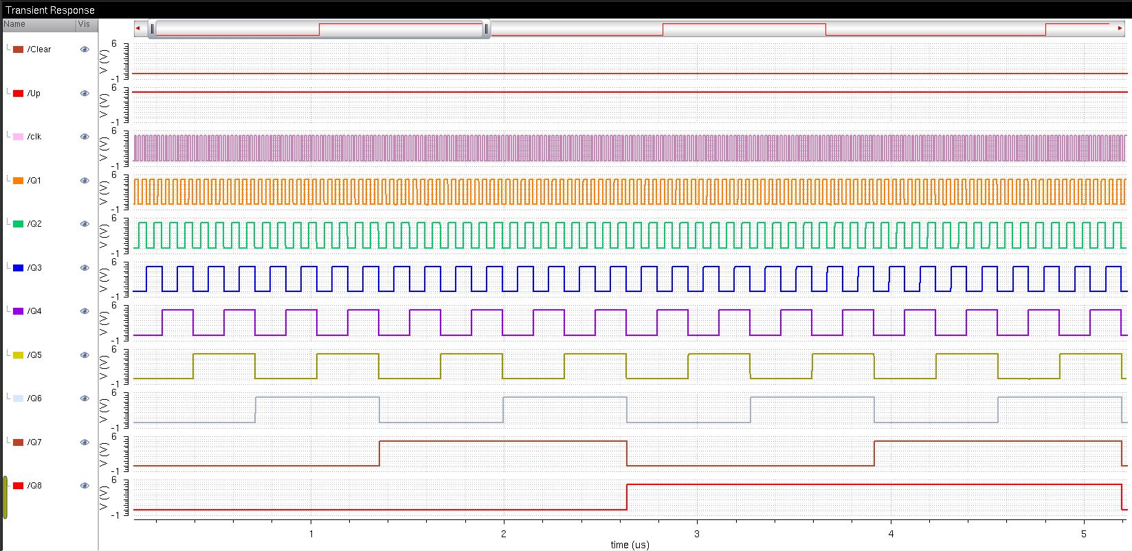 |
In the above simulation, it is seen the counting up operation of each bit (Q1, Q2, Q3, ... ,Q8) at
every rising edge. Bit changes (rising edge clock) occur every 5ns for
the least significant bit (LSB) Q1, whose rising edge represent bit
change in Q2, and so on.
The
next simulation shows operation of down counter. Before changing selector 'Up'
from high to low, current counter values should be set to zero, as seen
below at time 7us.
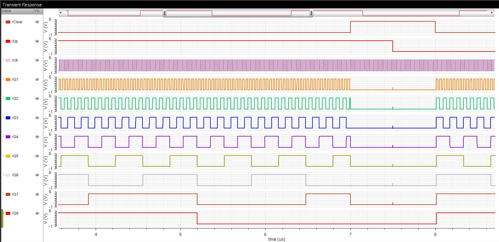
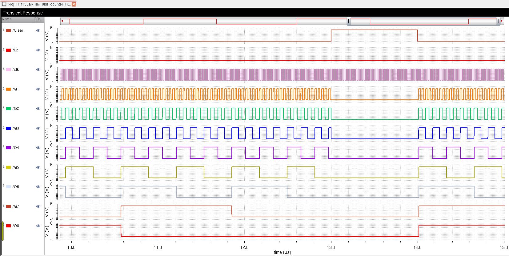
The next picture verifies all possible values of down counter and clear operation.
31-stage ring oscillator with buffer
Operation of the 31 ring oscillator is shown below, with its corresponding symbol
| sschematic | Symbol |
 | 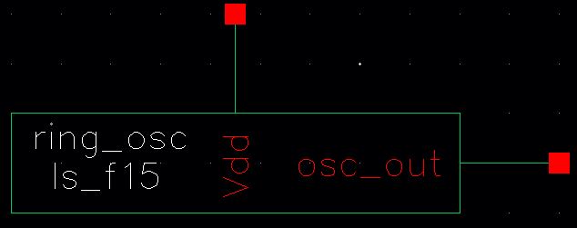 |
Array
of buses is implemented for the 30 connections between the 31
inverters. A common external vdd pin is connected to every inverter as
enable.
The frequency of the ring oscillator is calculated as follows:

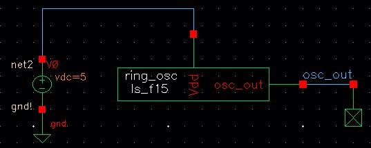
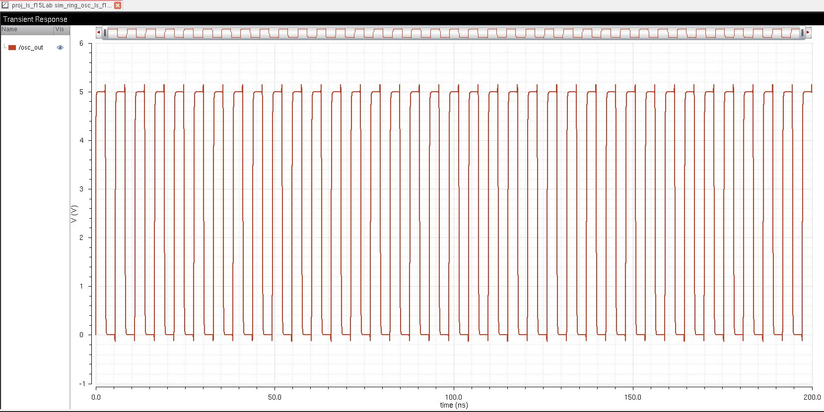
Operation
of the ring oscillator is verified in the following schematic and
simulation. For a proper simulation, the output 'osc_out' node is set
to zero.
| Schematic | Simulation |
 |  |
This
oscillator is to be connected through a buffer due to it will be
driving 20pF off-chip capacitance, so the buffer is implemented to
reduce the time delay.
| Buffer - Schematic | Buffer - Symbol |
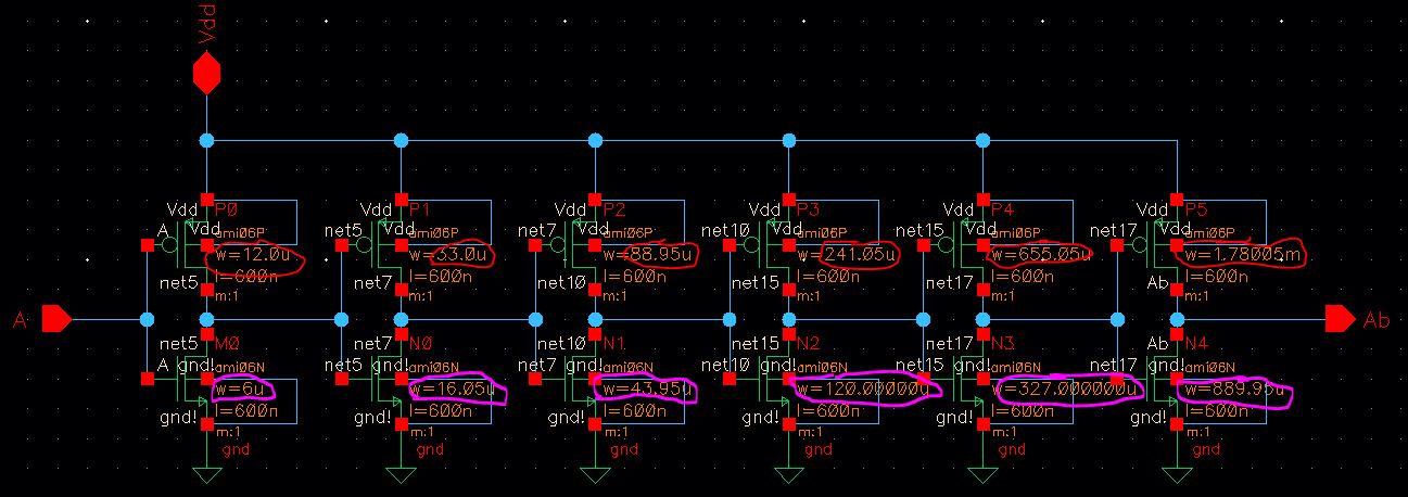 | 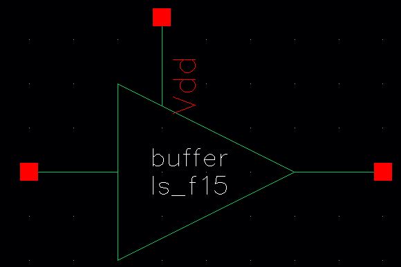 |
Even
though the number of inverters and size of each MOSFET were calculated
by applying appropiate theory from the book, this schematic would
represent a huge and unncessary implementation of a buffer for this simple
case, and will turn complicated the layout. Thus, the number of
inverters is reduced by making use of MOSFETs with larger dimensions (10-finger-MOSFET).
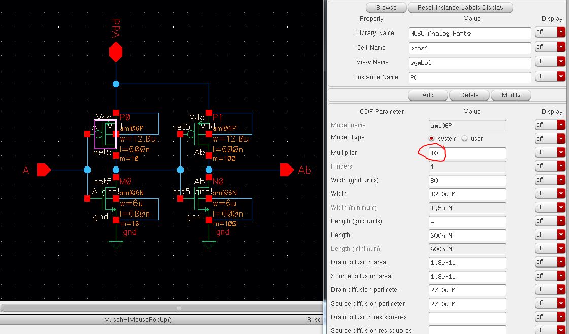
Implemention of the 31-ring oscillator with buffer is shown below.
| Schematic | Symbol |
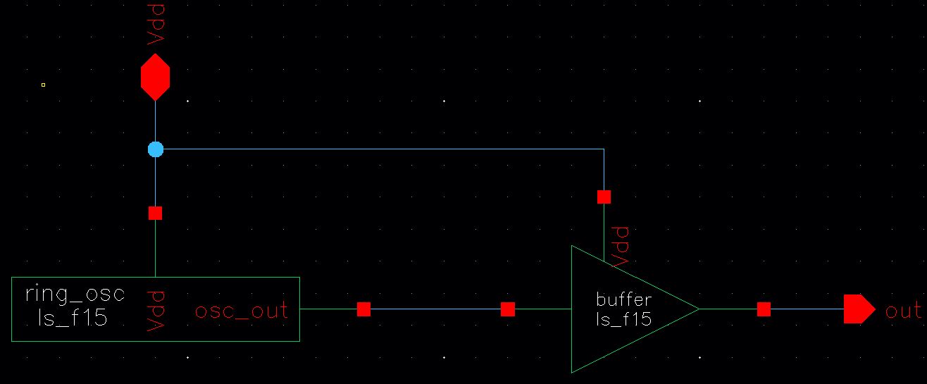 | 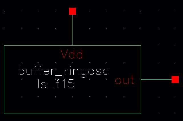 |
This circuitry is driving an off-chip 20pF capacitance load.
| Schematic | Simulation |
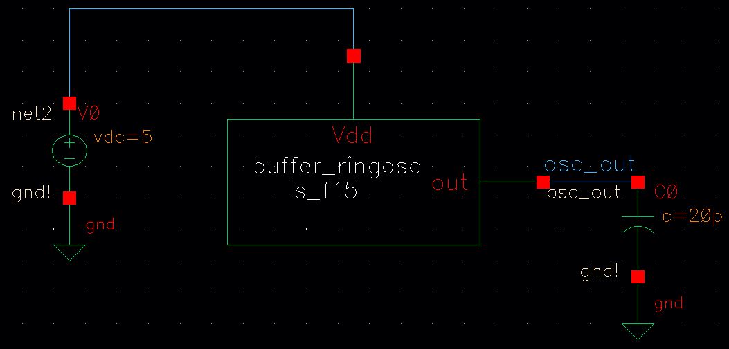 | 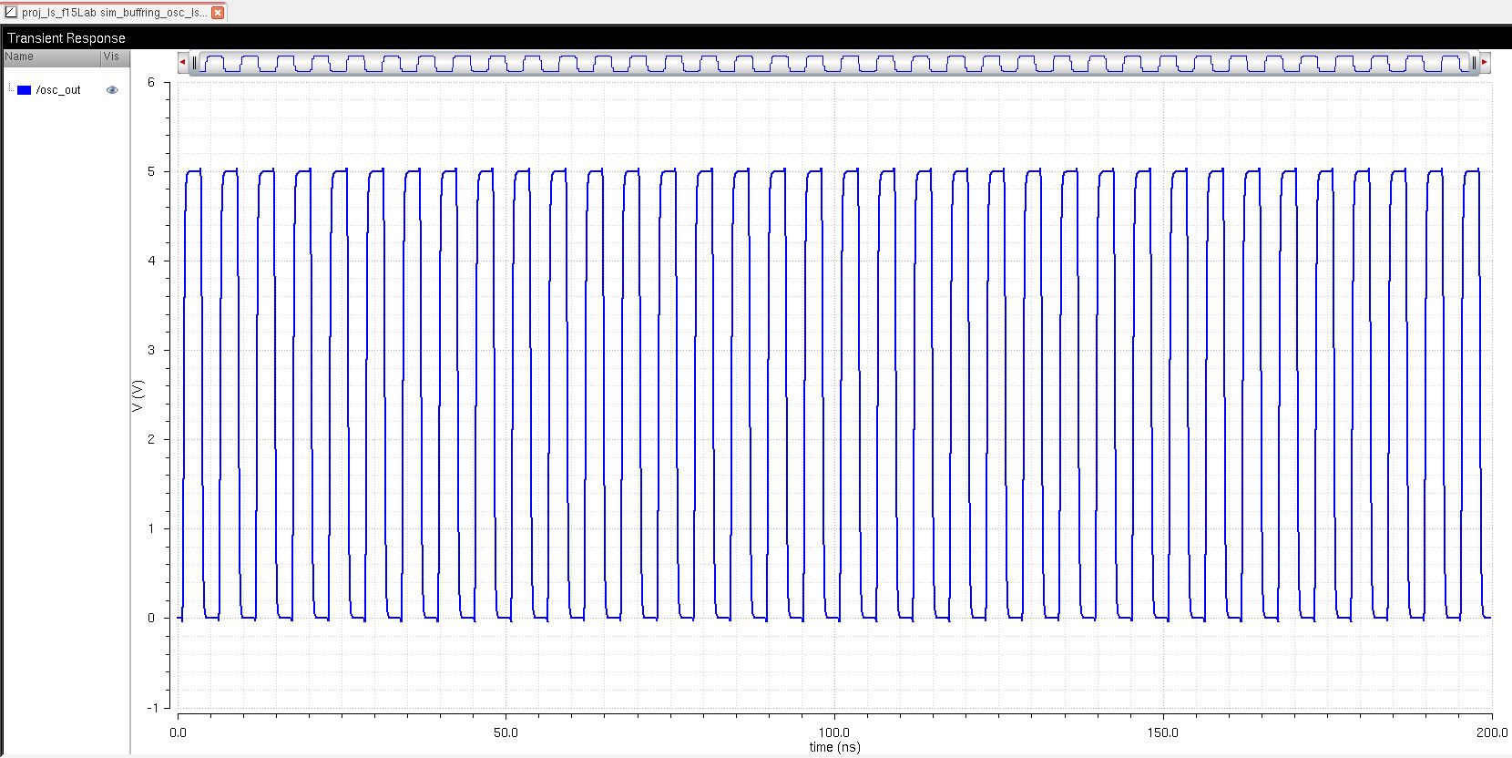 |
It
is observed that the implementation of the buffer works properly
obtaining the oscillating signal back, which means that the delay from
the external load can be fully compensated.
2 input, 6u/0.6u MOSFETs - NAND and NOR gates
NAND and NOR gates obey the following truth table
| A | B | A nand B | A nor B |
| 0 | 0 | 1 | 1 |
| 0 | 1 | 1 | 0 |
| 1 | 0 | 1 | 0 |
| 1 | 1 | 0 | 0 |
The following table shows the shematic, symbol, implemenation, and simulation of a 2 input NAND and NOR gates.
| Schematic | Symbol | Implementation | Simulation |
| NAND | 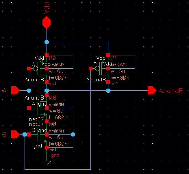 | 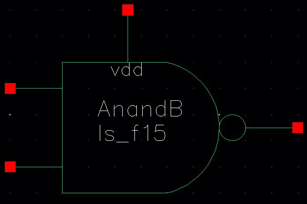 | 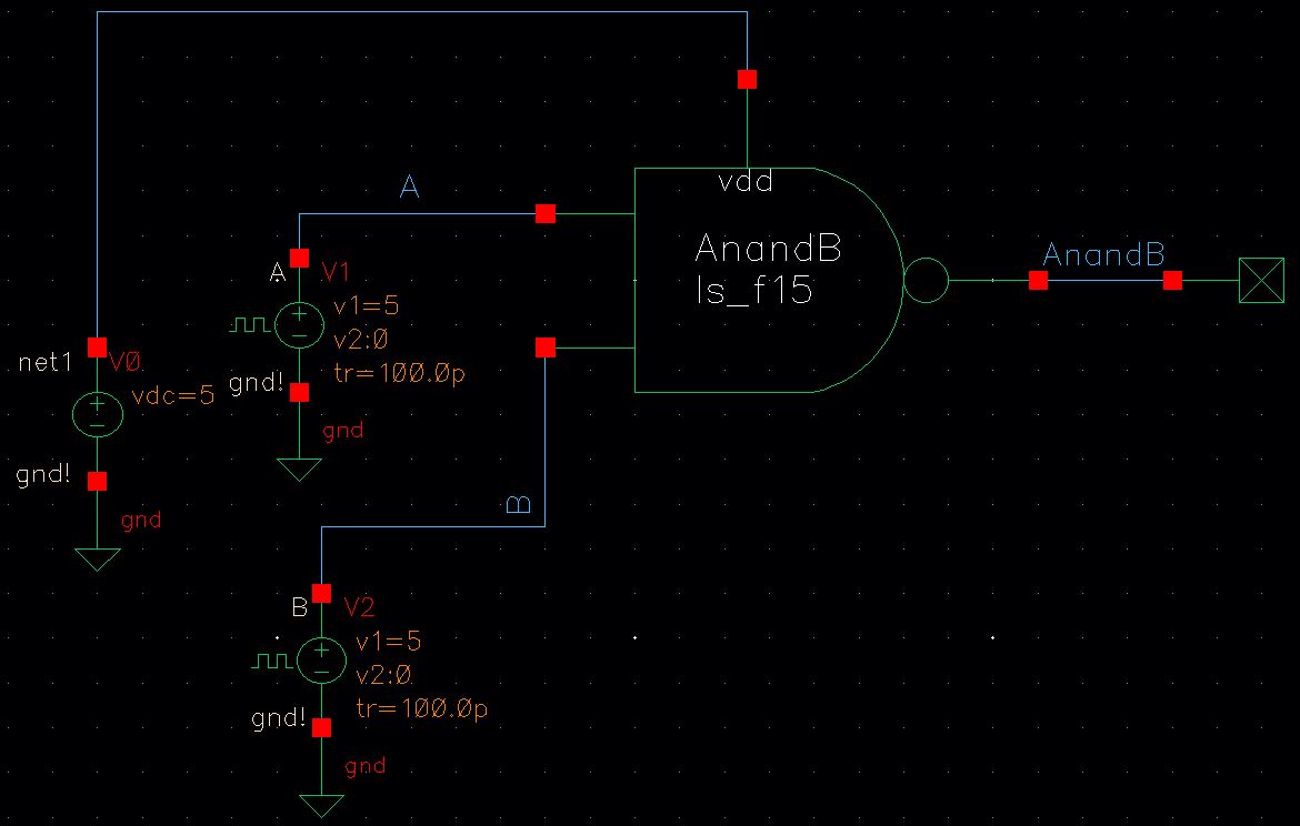 | 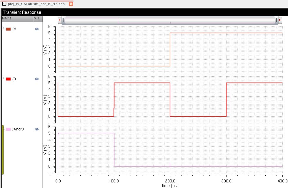 |
| NOR | 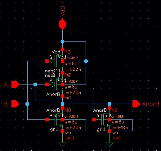 | 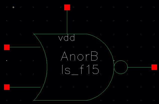 | 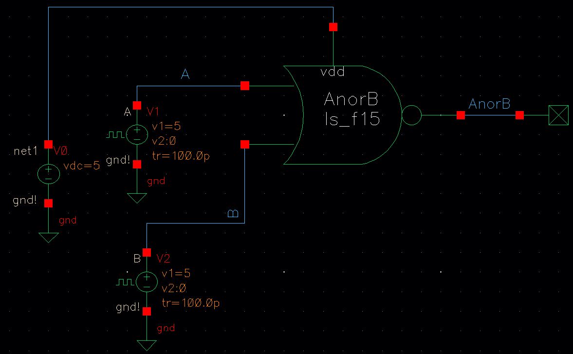 | 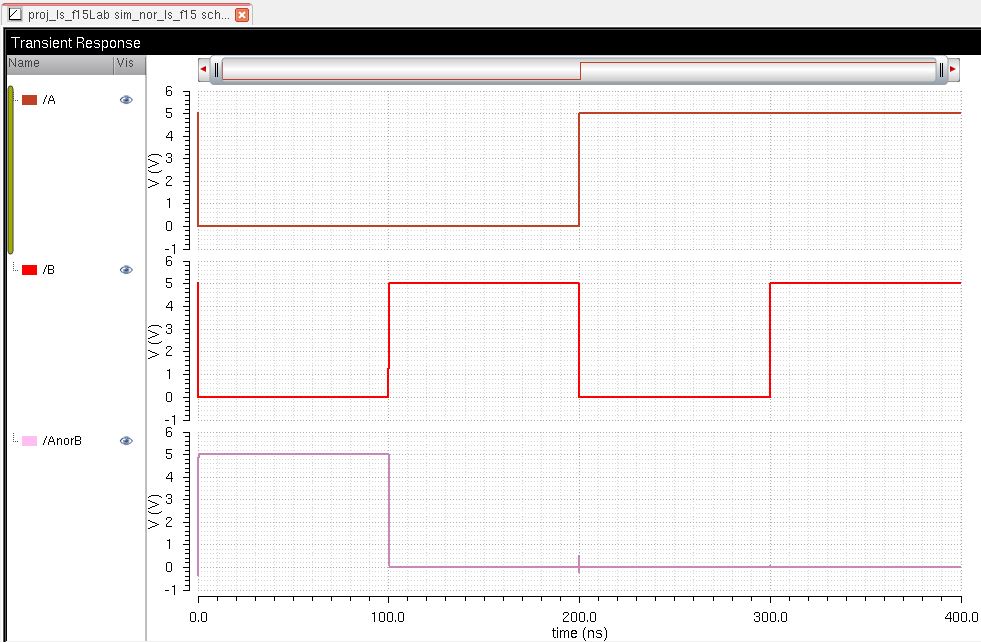 |
It is observed that the operation of both NAND and NOR gates was verified properly.
12u/6u Inverter (L=600n)
The following table shows the shematic, symbol, implemenation, and simulation of an inverter.
| Schematic | Symobol | Implementation | Simulation |
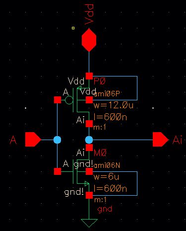 | 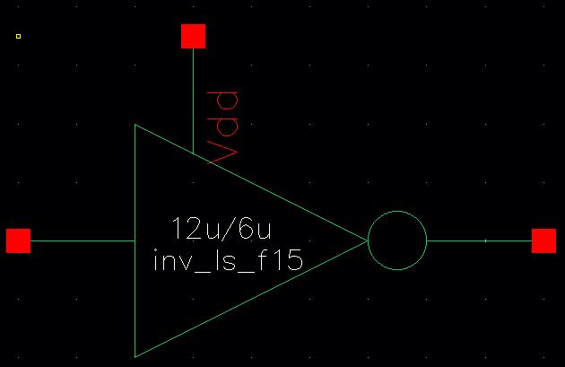 | 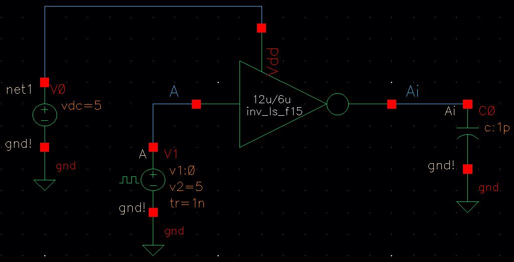 | 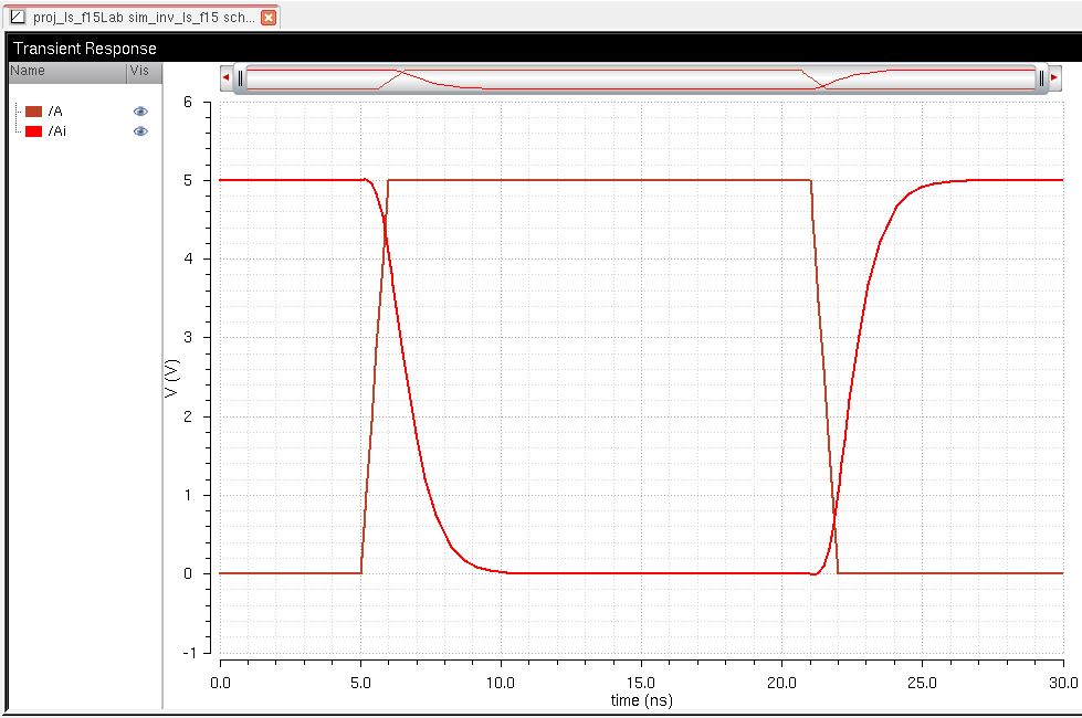 |
4 terminal 6u/0.6u NMOS and PMOS with bonding pads
This
section corresponds to the implementation and operation of an NMOS and
a PMOS where each terminal is connected to a bond pad, being one bond
pad a common ground for both.
The bondin pads connected to the
MOSFET measures 75um square of metal 3 and 60um square of glass layer.
The bonding pad layout, schematic, and symbol are shown below.
| Layout | Schematic | Symbol |
Bonding
Pad |  |  |  |
The following table shows the shematic, symbol, implemenation, and simulation of the NMOS and PMOS.
| Schematic | Symbol | Implementation | Simulation |
| NMOS | 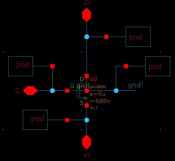 | 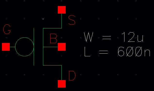 | Id vs VGS
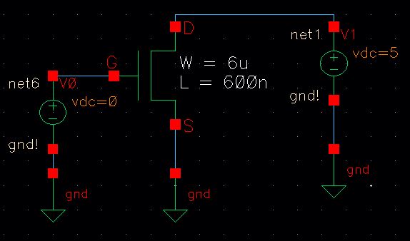 | 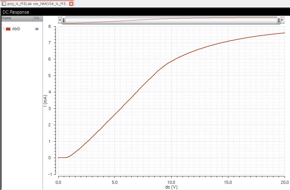 |
| PMOS | 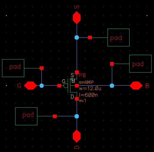 |  | Id vs VSG
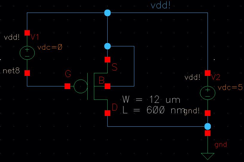 | 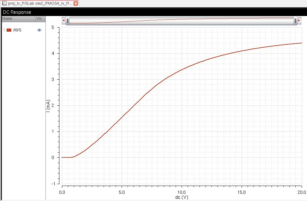 |
| Implementation | Simulation |
| NMOS | Id vs VDS (VGS from 0 to5V)
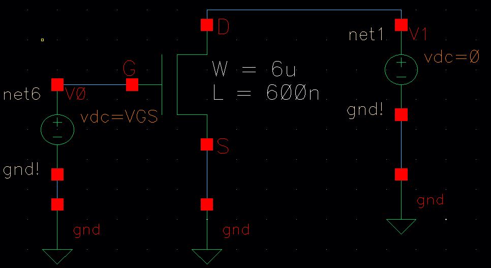 | 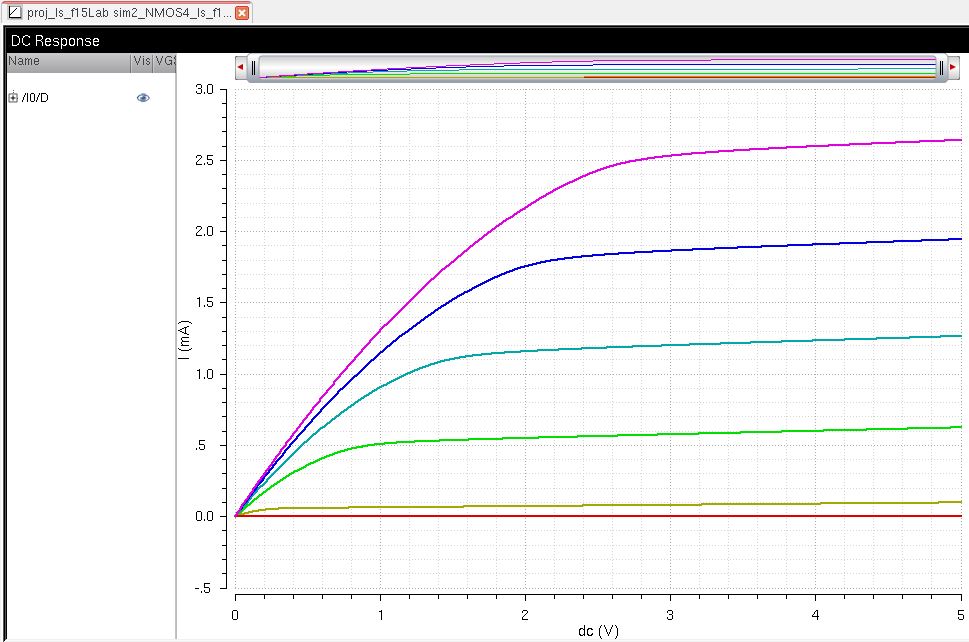 |
| PMOS | Id vs VSD (VSG from 0 to5V)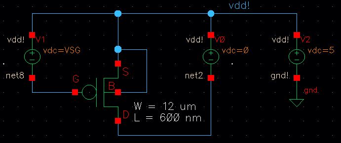 | 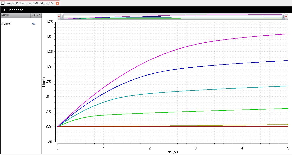 |
25k ohms resistor implemented using n-well
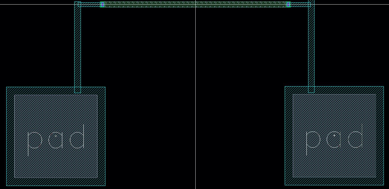
Both
sides of the 25k resistor are connected to bond pads, being one of them
ground (gnd). The n-well size of the resistor was 137.4umx4.5um.
| Layout | Schematic |
 |  |
Voltage divider using 10k and 25k resistors
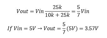
The voltage divider operation:
| Schematic | Symbol | Implementation | Simulation |
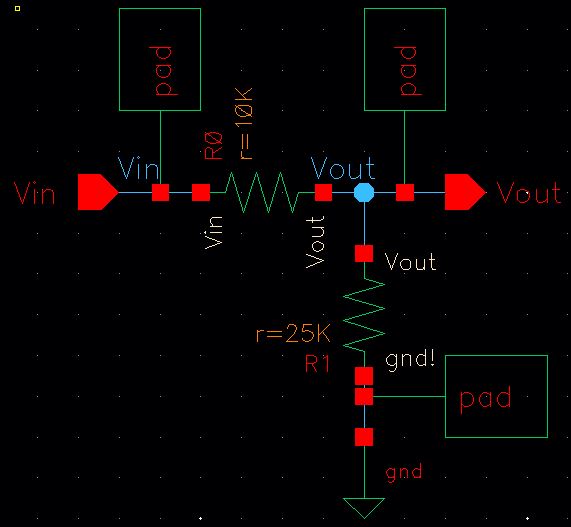 | 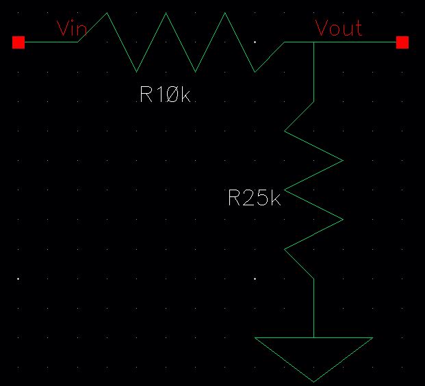 | 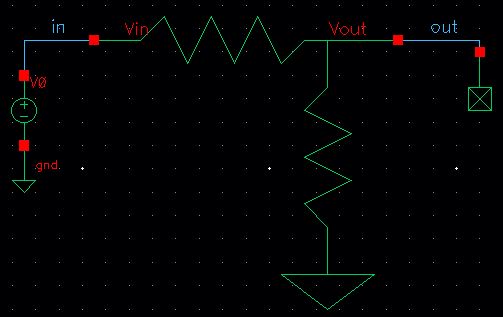 | 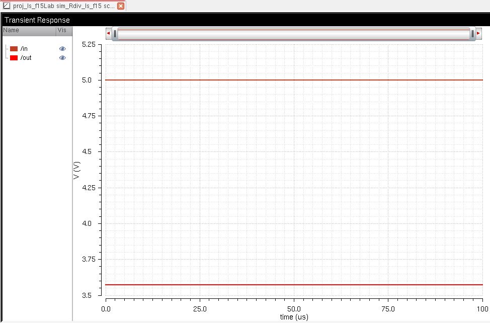 |
It is seen in the simulation that the operation of the voltage divider works as expected.
This ends the first part of the laboratory project.
----------------------------------------------------------------------------------------------------------------
Part 2: The
second part of the project requires us to layout, DRC, and LVS all the
schematics designed in the first part, as listed below:
- Design of an 8-bit resettable (input "clear") up/down counter
- The outputs of your counter should be buffered before connecting to a pad
- A 31-stage ring oscillator with a buffer for driving a 20 pF off-chip load
- NAND and NOR gates using 6/0.6 NMOSs and PMOSs
- An inverter made with a 6/0.6 NMOS and a 12/0.6 PMOS
- Transistors,
both PMOS and NMOS, measuring 6u/0.6u where all 4 terminals of each
device are connected to bond pads (7 pads + common gnd pad)
- Note
that only one pad is need for the common gnd pad. This pad is used to
ground the p-substrate and provide ground to each test circuit
- A 25k resistor implemented using the n-well (connect between 2 pads but we also need a common gnd pad)
- Using the 25k resistor laid out above and a 10k resistor implement a
voltage divider (need only 1 more pad above the ones used for the 25k
resistor
8-bit resettable up/down counter
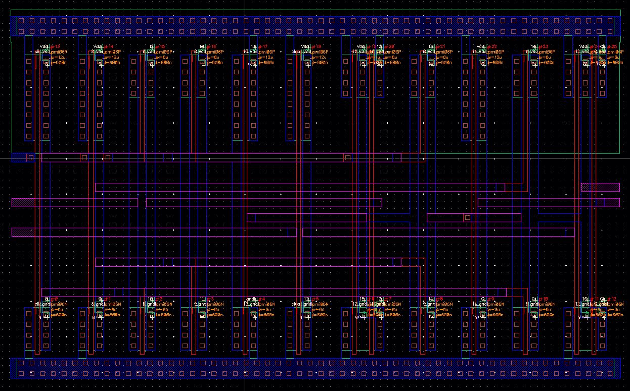
For the D-flipflop, layout and extracted view are shown below.
Layout
| Extrated view |
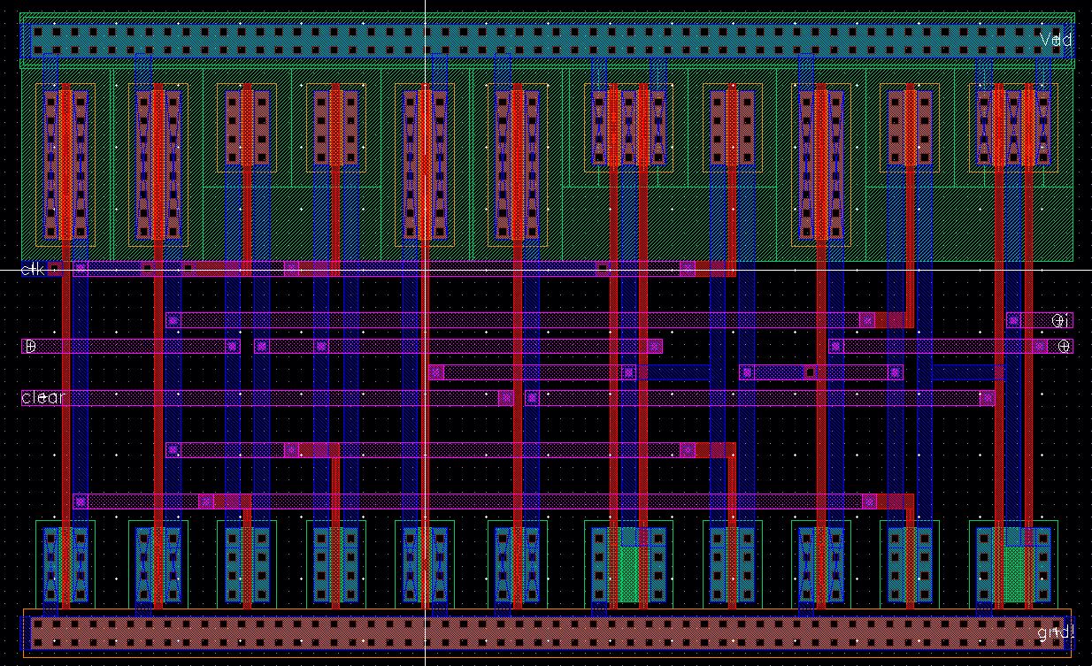 |  |
Then, DRC to verify no errors were found.

Now, LVS (layout vs schemactic) can be run.
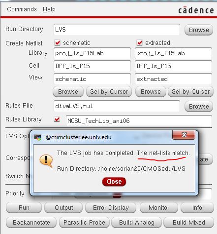
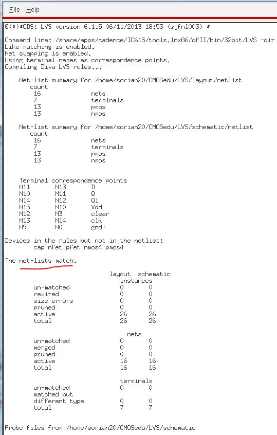
It is shown that both circuits match.
The next componenent to be layout is the 2-to-1 MUX, used to implement the 8 bit counter.
| Layout | Extracted view | DRC | LVS | LVS output file |
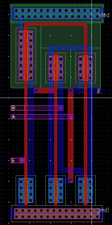 | 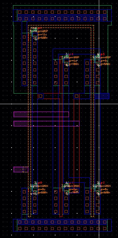 |  | 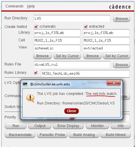 | 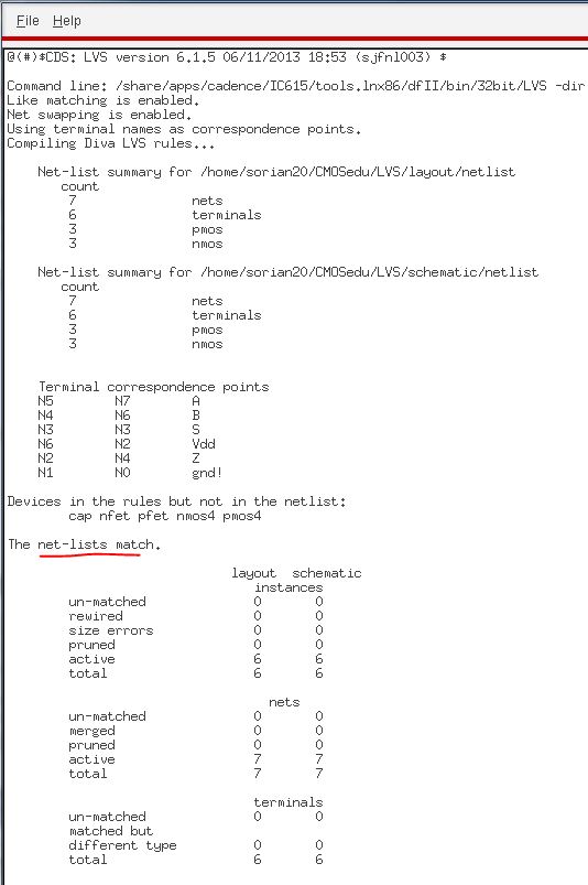 |
It is seen that the DRC shows no errors, and both the schematic and extracted view match when LVS.
Now, let's implement this two block in the 8-bit up/down counter.

The layout and extracted view are shown below.


Zooming
in the layout to see in detail the implementation of D-flipflop and MUX
on each stage (Q2 for this case, between yellow lines)
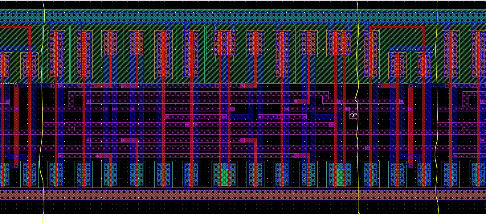
DRC to verify no errors were found.

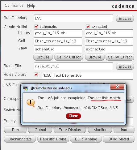
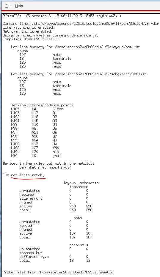
Running LVS (layout vs schematic), it is shown that both circuits match.
To verify the functionality of the layout, extracted view is then simulated.
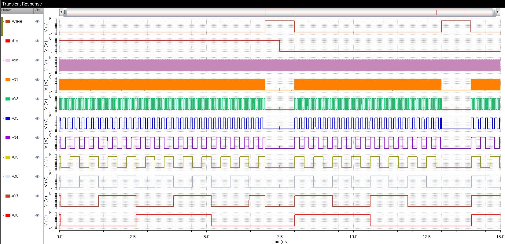
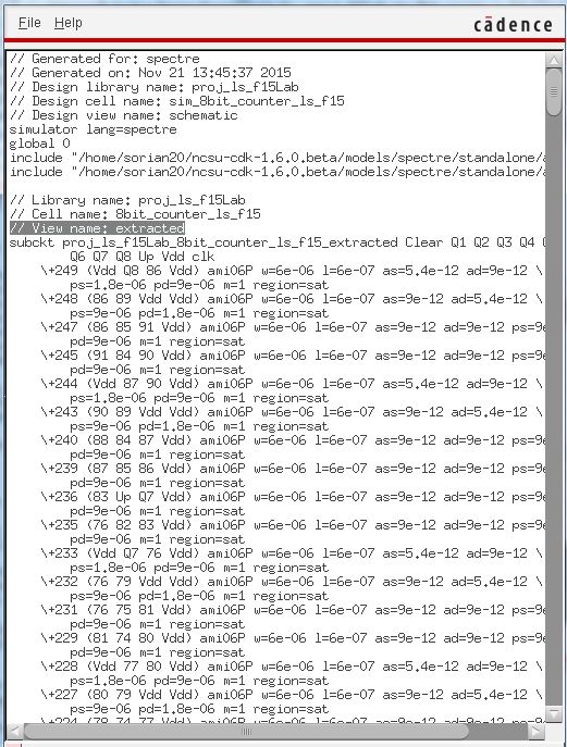
Simulation of the layout worked properly based on previous simulations!!
12u/6u Inverter (L=600n)
Layout, extracted view, DRC, LVS of the previously designed inverter is shown below.
| Layout | Extracted view | DRC | LVS | LVS output file |
 |  |  | 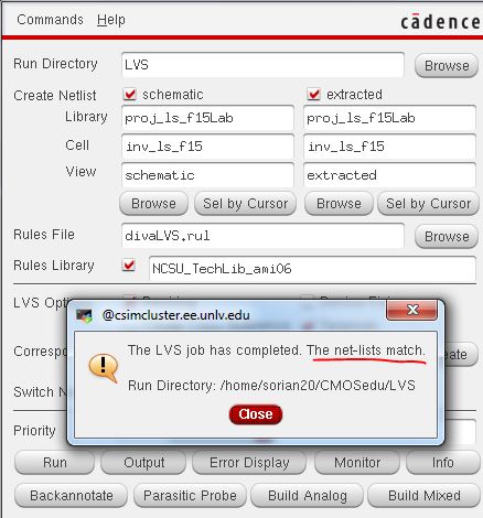 | 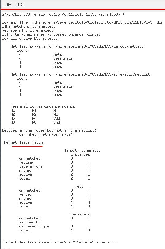 |
DRC shows no violated errors, and both the layout and schematic matched in the LVS!!
31-stage ring oscillator with buffer
The ring oscillator is layout first as shown in the table below.
| Layout |
 |
| Extracted view |
 |
DRC to verify no errors were encountered, and LVS the run.
The buffer is now implemented in layout.
| Layout |
 |
| Extracted view |
 |
Zooming in the extracted viw to see the details in the MOSFETS used.
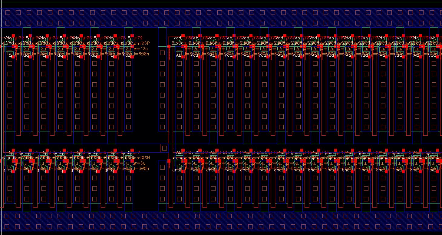
DRC to verify no errors were found and LVS to verify both schematic and layout match.
The buffer is implement at the output of the rign oscillator per project requirements.
| Layout |
 |
| Extracted view |
 |
| DRC (design ruler check) |
 |
| LVS (layout vs schematic) |
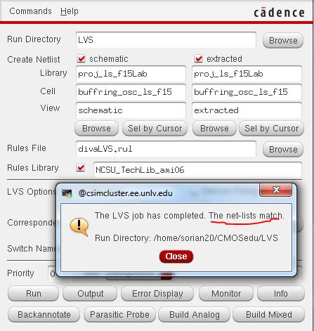 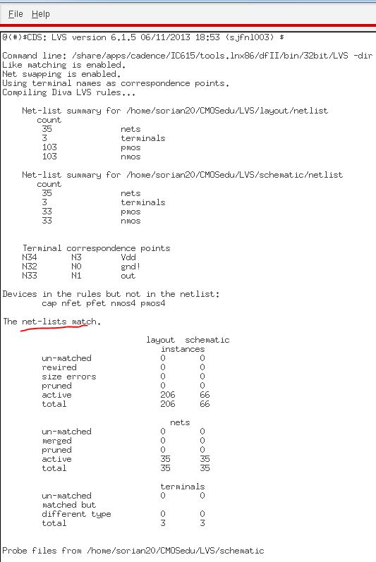 |
Once again, DRC shows no erros, and LVS matches both the schematic and layout.
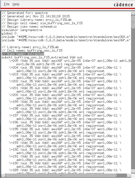
To verify the functionality of the layout, extracted view is then simulated.

2 input 6u/0.6u - NAND and NOR gates
The following table shows the layout, extracted view, DRC, and LVS for both 2 input NAND and NOR gates.
| Layout | Extracted view | DRC | LVS | Output file |
| NAND |  |  |  | 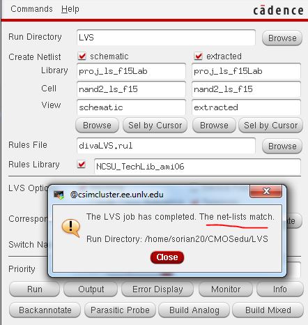 | 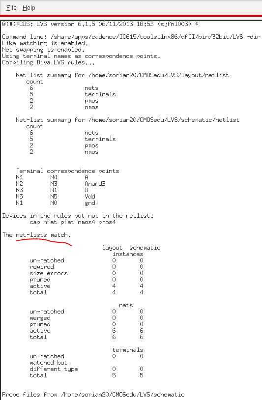 |
| NOR |  |  |  | 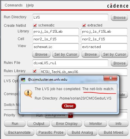 | 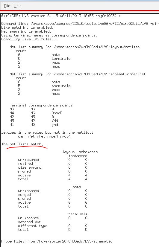 |
For both NAND and NOR gates, it is seen that DRC and LVS run with no errors.
To verify the functionality of the layouts, extracted views are simulated in spectre.
| Simulation | Spectre file |
| NAND |  | 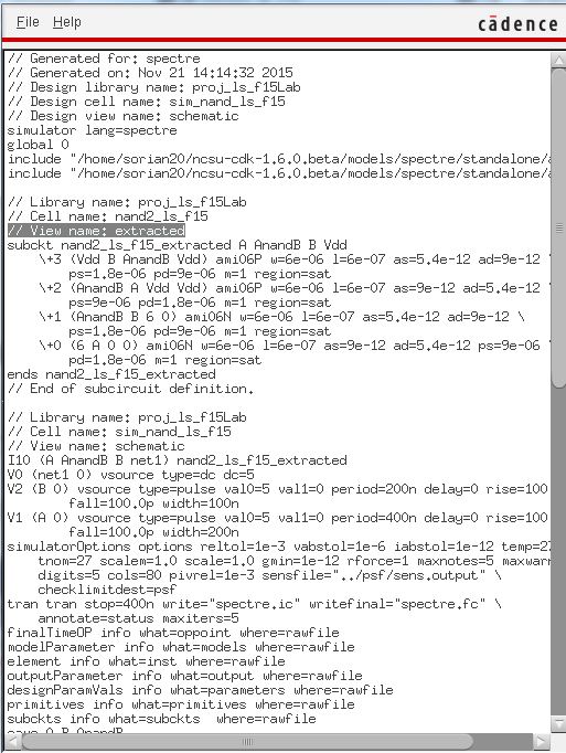 |
| NOR |  | 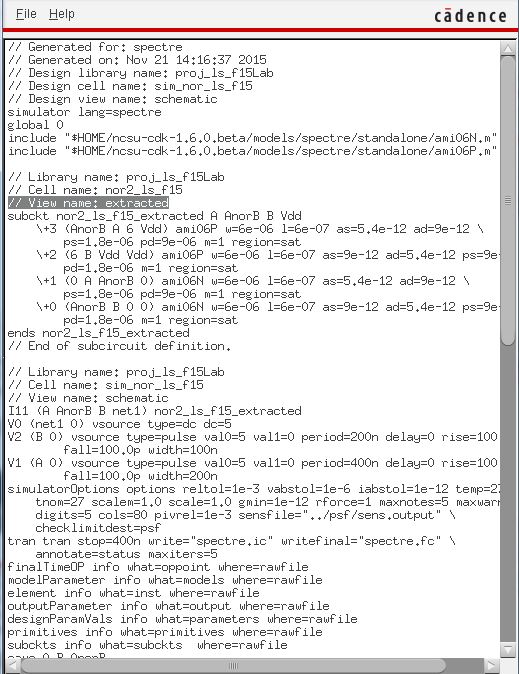 |
4 terminal 6u/0.6u NMOS and PMOS with bonding pads
Layout of NMOS and PMOS devices are shown in the follwing table with bonding pads.
Now LVS is performed.
| Extracted view | LVS | Output file |
| NMOS | 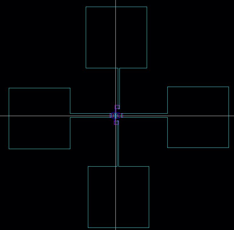 | 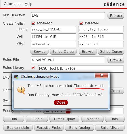 | 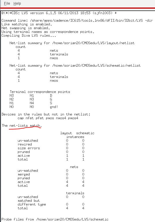 |
| PMOS | 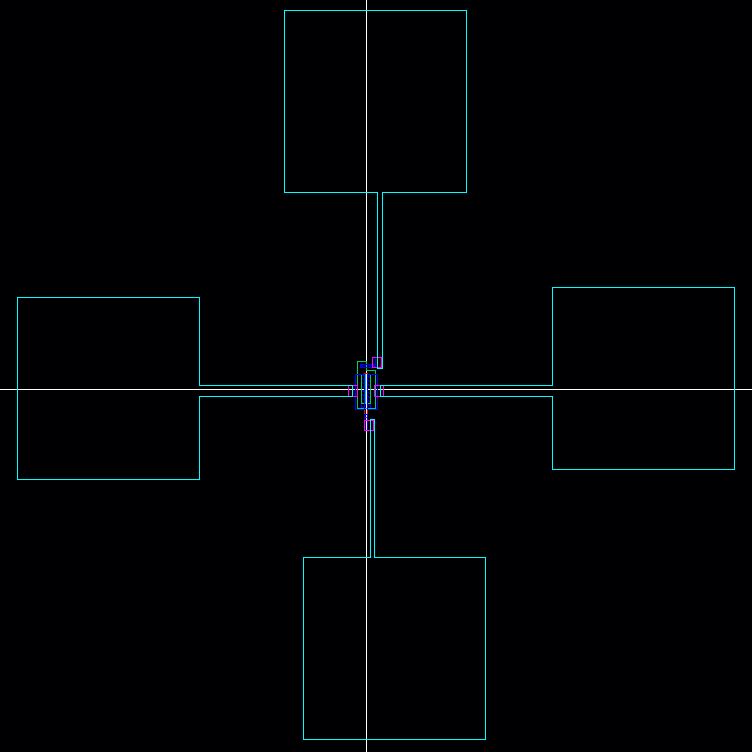 | 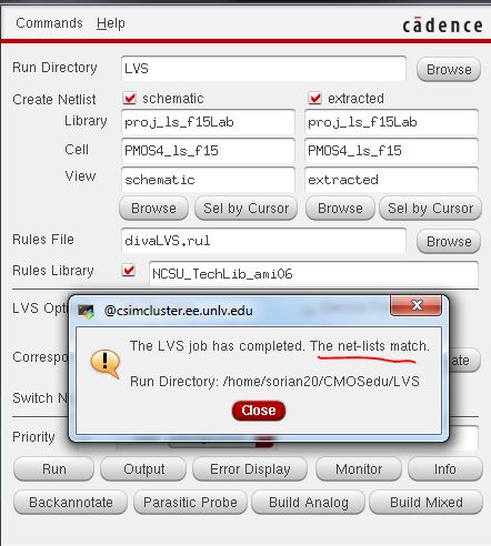 | 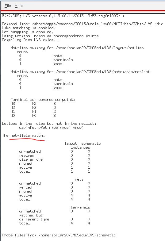 |
It is observed that the netlist matches for both NMOS and PMOS !!
25k ohm resistor implemented using n-well
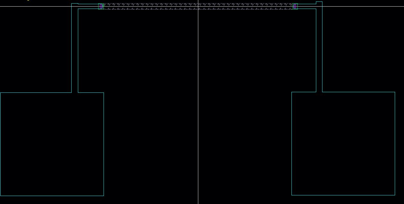
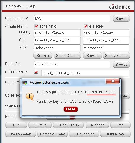
Layout,
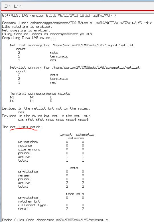
extracted view, DRC, and LVS of 25k resistor are listed below.
Dimensions used in the layout are 4.5u x 137.4u (high res on n-well).
| Layout | Extracted view | DRC | LVS | Output file |
 | 
 |  |  |  |
Voltage divider using 10k and 25k resistors
10k and 25k nwell resistor are laid out per project requirements. Dimensions for the 10k nwell resistors: 4.5u x 56.1u.
| Layout | DRC |
| 10k |  |  |
The next table implements the 10k and 25k resistor in a voltage divider.
LVS is then run.
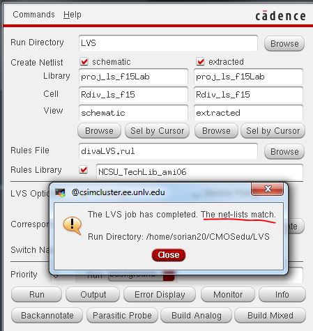
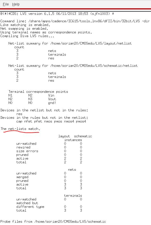
The netlist matches! To verify the layout works, the extracted view is simulated in spectre.
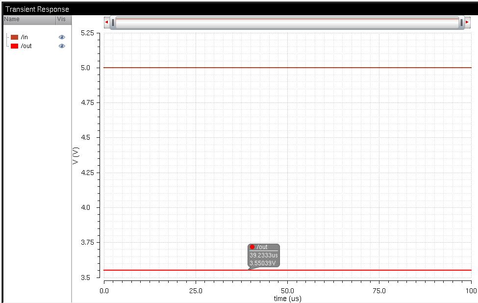
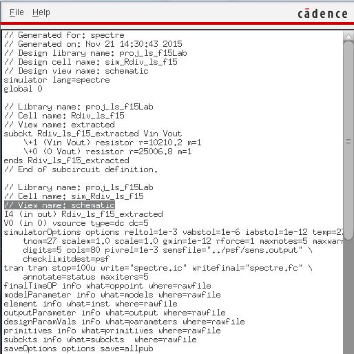
It
is seen from this simulation that the output value corresponds to 3.55V
instead of 3.57V, as obtained from the schematic. This due to the
resistance values from both resistor were approximately 10k and 25k,
but not exactly, causing some deviation in the expected output value,
but still acceptable for our purposes.
----------------------------------------------------------------------------------------------------------------
As
indicated, all cells were named adding my intials and semester
(LS_f15). All cells and simulations used in this project can be
downloaded here.
As always, back up of this lab was saved on my portable USB, Google drive account, and in the CMOS account drive.
-------------------- Go back
Return to EE421L - Student Lab Reports
Return to EE421L - Fall 2015