Lab 7 -
EE 421L
Digital Integrated Circuit Design
Author:
Matthew Meza
Email:
mezam11@unlv.nevada.edu
November 2, 2015
Using busses
and arrays in the design of word inverters, muxes,
and high speed adders!
Pre-lab work
- Back-up
all of your
work from the lab and the course.
- Go
through Tutorial
5 seen here.
- Read through the
entire lab before starting it.
Lab Description
In
this lab we will design, layout, and simulate an multiple bit gates and
devices including muxes, demuxes,
inverters, and high-speed adders.
Lab Requirement
- Create
a 4-bit inverter including a schematic and symbol.
- Test
the 4-bit inverter with simulations.
- Show
how a capacitive load influences the delay and rise/fall times.
- Create
schematics and symbols for an 8-bit input/output array of: NAND, NOR,
AND, inverter, and OR gates.
- Provide
a simulation using these gates.
- Create
a 2 to 1 DEMUX/MUX along with a symbol
- Include
a simulation of the operation of the DEMUX/MUX.
- Create
an 8-bit word 2-to-1 DEMUX/MUX schematic and symbol.
- Include
simulations to verify operations
- Draft
the schematic and layout of the full adder seen in Fig. 12.20 using
6u/0.6u devices
- Include
an adder symbol and use it to draft an 8-bit adder, then layout the
8-bit adder.
Simulate the operation of the 8-bit adder and show that it DRC's and
LVS's correctly!
Pre-Lab Excercises
Ring
Osccilator Schematic

Notice how the BUS wires are labeled
in order to create the ring oscillator!
|
Small
section of the Ring Oscillator Layout
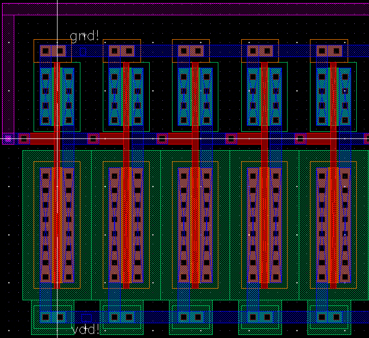 |
Full
Layout of the Ring Oscillator

The layout is so large that it is hard to realize small details |
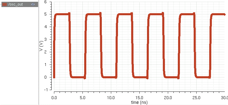
Simulation
of the Ring Oscillator
 |
Post-Lab Excercises
4-Bit Inverter
4-Bit
Inverter Schematic
 |
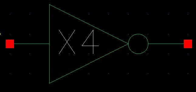
Symbol
used for the 4-bit Inverter Schematic
 |
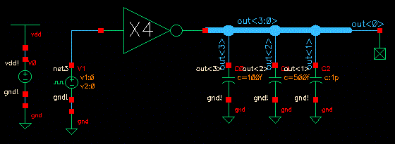
Simulation
Schematic using the 4-bit symbol
 |
Simulation
of the 4-bit inverter!
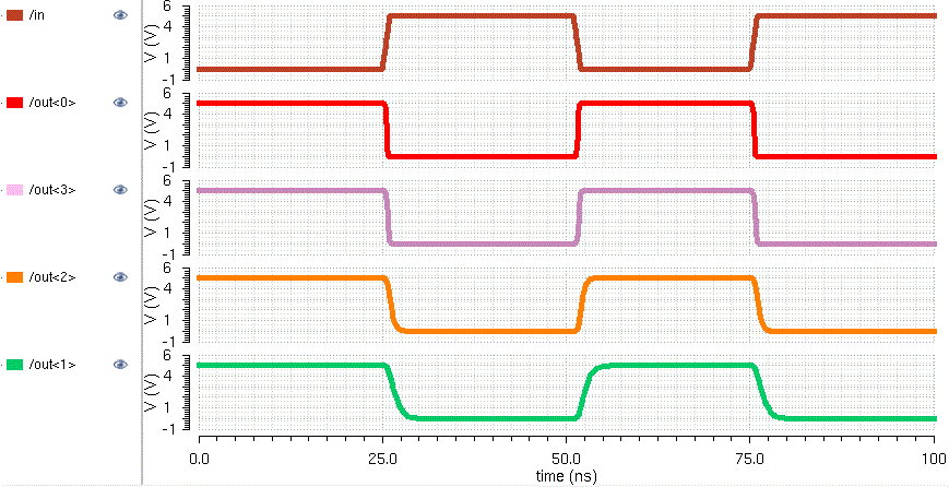 |
From the simulation we can see how the different valued capacitor loads
affect the delay times and rise/fall times.
The top plot shows the clock in the simulation, the second plot shows
the output of the
inverter without a capacitive load.
The rest of the plots show the
output of the inverter with increasing capacitive load. Notice how the
last plots
have slower fall/rise time!
8-Bit Gates!
8-Bit Gates!
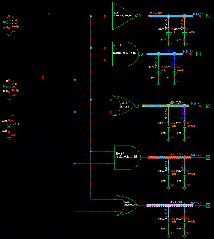
Included is the inverter, NAND, NOR, AND, and OR gates! |
Close up of the simulation
schematic!
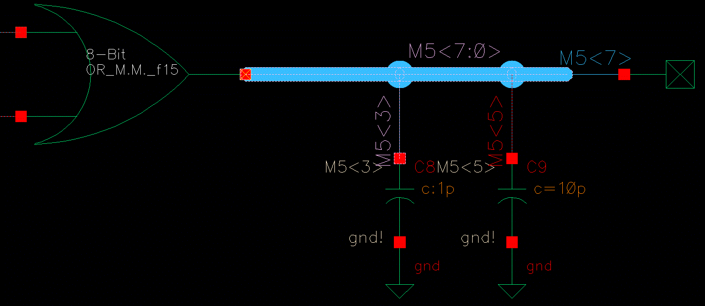
There are two load capacitors used for each gate to demonstrate that
they are multiple bits! |
Simulation!
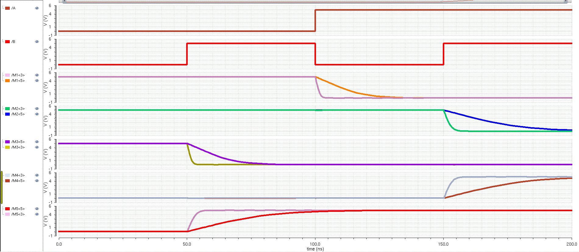
Shown
above are the simulations of the 8-bit gates with each gate driving 2
different valued capacitors from 2 of the total 8 bits!
The first
two plots above show the A input and B input. The rest of the plots
show the gate outputs. Notice how one of each gate outputs
has a very slow fall/rise time; this is caused by the large capacitive
load!
2-to-1 MUX/DEMUX
Two transmission gates are used
to create a
2-to-1 mux/demux
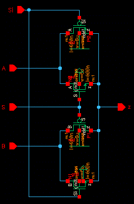 |
Symbol for the 2-to-1 mux/demux
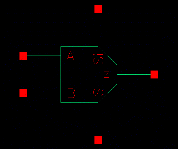 |
Simulation schematic using the
2-to-1 mux/demux symbol
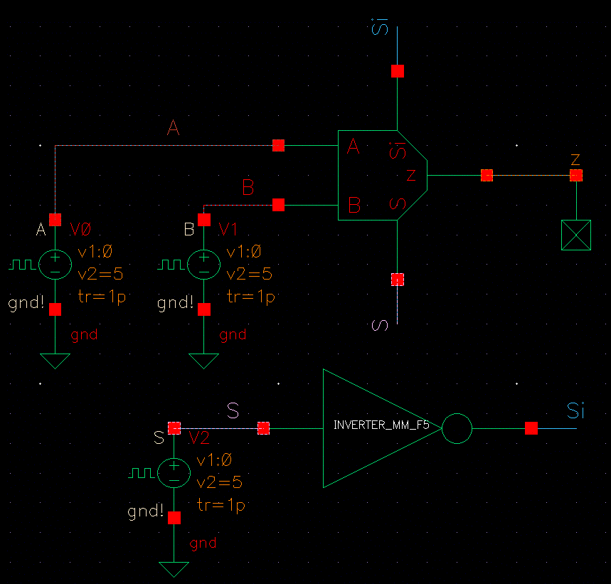 |
Simulation of the mux/demux!
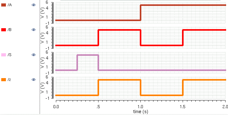
|
8-Bit Word 2-to-1 MUX/DEMUX
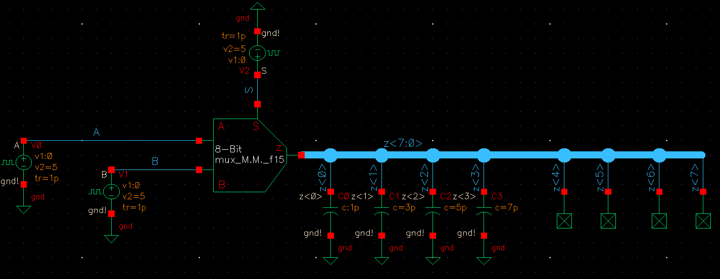
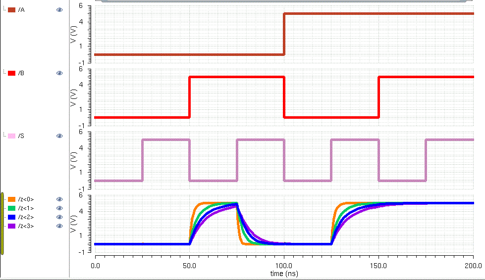
Simulation of 8-bit 2-to-1 Mux/Demux
4
output bits of the MUX/DEMUX were connected to varied capacitive loads.
Notice how the last plot shows several pulses with varied
RC time constants (different
rise/fall times).
1-Bit High Speed Full Adder
High Speed Full Adder Schematic
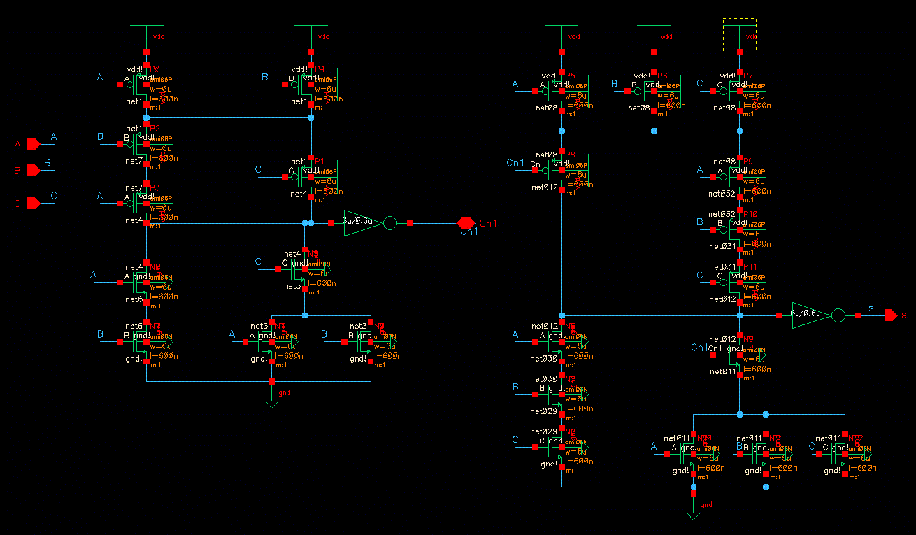 | Layout of the 1-Bit Full Adder
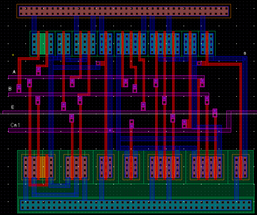 |
Proof of LVS and DRC

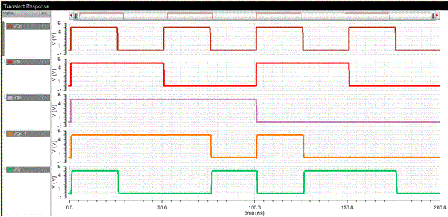
 | Simulation of 1 Bit Full Adder!
 |
8-Bit High
Speed Full Adder
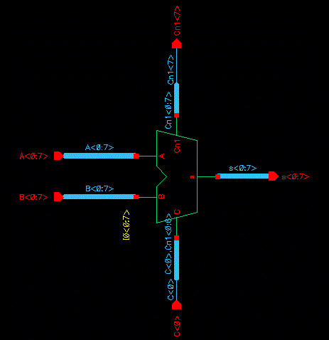
Schematic of the 8-Bit Full Adder!
Complete Layout!

Proof of DRC/LVS


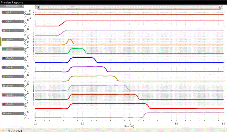
Simulation of 8-bit Full Adder
Return
to EE 421 Labs