Lab 5 - EE 421L
Digital Integrated Circuit Design
Post-Lab Excercises
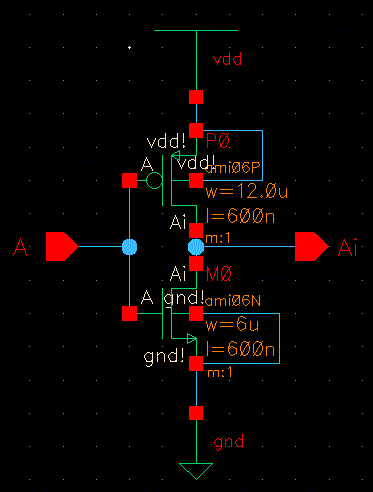
| Inverter1,
M=1 |
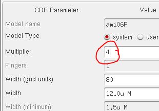
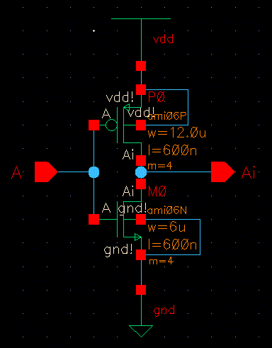
Inverter2,
M=4 (four devices in parallel) |
Inverter1
Schematic, DRC, LVS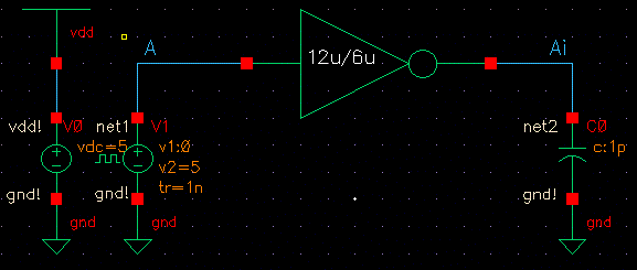  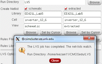 |
Inverter1
Layout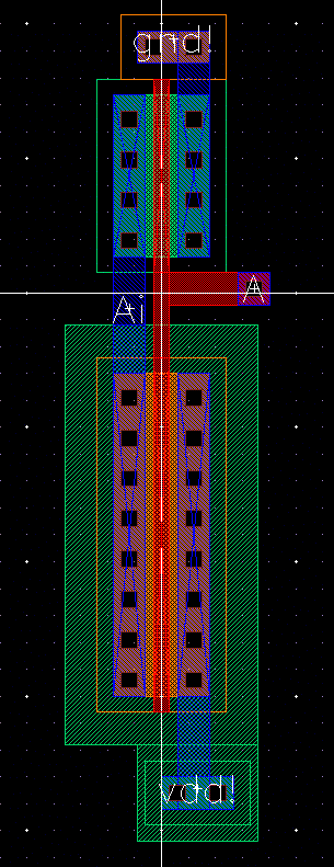 |
Inverter2
Schematic, DRC, LVS  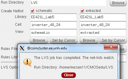 |
Inverter2
Layout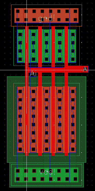 |
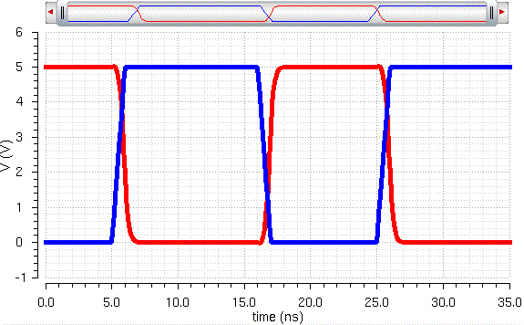
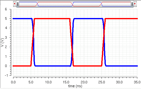 100fF load; Blue - output! |
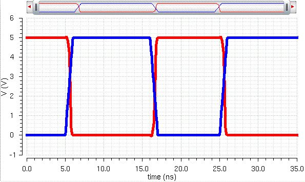 100fF load; Red - output! |
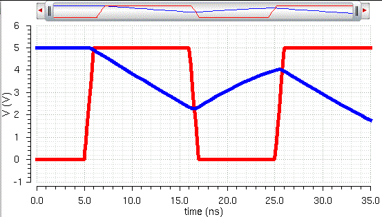
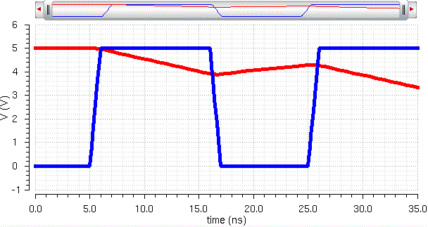
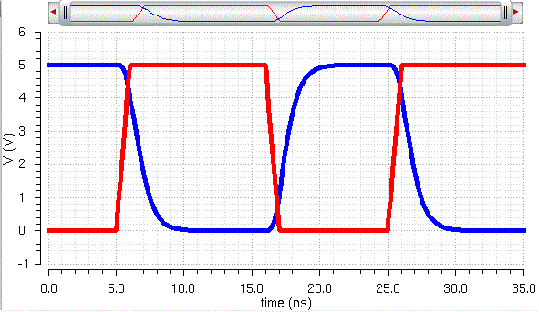 1pF load; notice the RC behavior. |
 1pF load; the larger MOSFETS are able to supply more current than the smaller MOSFETS in Inverter 1 |
 10pF; the inverter is no longer able to supply sufficient current. |
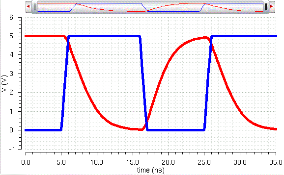 10pF load; notice the RC behavior, the inverter not able to supply enough current fast enough. |
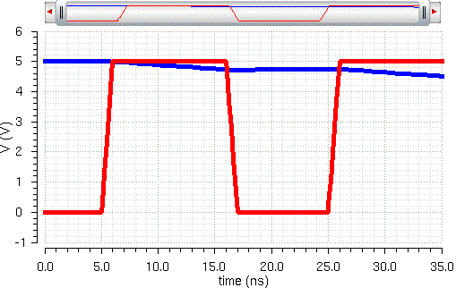 100pF; the inverter is completely useless at this load. |
 100pF; the inverter is no longer able to supply sufficient current. |