Lab 3 - EE 421L
Digital Integrated Circuit Design
Author:
Matthew Meza
Email:
mezam11@unlv.nevada.edu
September 14, 2015
Layout
of a 10-Bit digital-to-analog converter (DAC)
Pre-lab work
- Back-up
all of your previous work from the lab and the course.
- Finish Tutorial 1 seen here.
Lab Description
In
this lab we'll use n-well resistors to implement a 10-bit DAC.
Our
design is based upon the topology seen in Fig. 30.14, below, in
the CMOS book.
The
controlling input bits seen below come from the ADC, in other words the
inputs to the DAC are the left side of the 2R resistors.
Lab Requir
This lab will focus on the layout of the 10-bit
DAC you designed and simulated in Lab 2
- Use
the n-well to layout a 10k resistor as discussed in Tutorial 1
- Discuss,
in your lab report, how to select the width and length of the resistor
by referencing the process information from MOSIS
- Use
this n-well resistor in the layout of your DAC
- Discuss,
in your lab report, how the width and length of the resistor are
measured
- Ensure
that each resistor in the DAC is laid out in parallel having the same
x-position but varying y-positions (the resistors are stacked)
- All
input and output Pins should be on metal 1
- DRC
and LVS, with the extracted layout, your design (show the results in
your lab report)
- Zip
up your final design directory and place it in the lab3 directory, with
a link on your lab report, so the grader can examine both the
layout and schematic (and simulations)
Post-Lab Excercises
In order to layout the 10-bit DAC designed in Lab 2, we must first lay
out a resistor. We will use one resistor (one value) for the
design of the DAC. To layout the resistor, we must know the sheet
resistance of the n-well! Off of the MOSIS website we can find that the
sheet resistance is approximately 800 ohm! Keep in mind that we have a
design rule with minimum width of 3.6u. Shown below is the resistor
laid out with a width of 4.5u. To find the length needed we can use the
following equation: L = 10K*W/800Ohm! In addition, pressing K will
bring up a ruler which can be used to measure the length of the N-Well
or any other element/instance. Opening up the properties of the N-well
will also show the length/width! Notice the ruler in the image below to
measure the length of the N-well resistor!
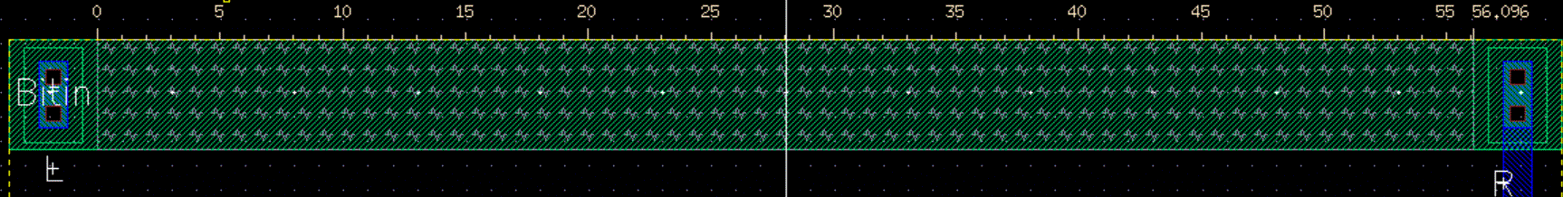
The Layout
of my DAC bit!
Notice how I use two 10k resistors in series for the
20k resistor in the DAC bit! I layed a seperate DAC bit so
that my DAC layout would be simpler and easier to modify!
|
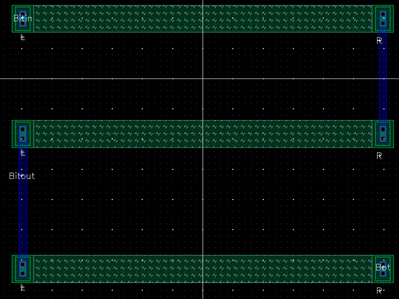
The Layout
of my DAC
Notice how I connect the bottom of the DAC to another
10K resistor! The image above shows the bottom part
of the complete DAC layout.
|
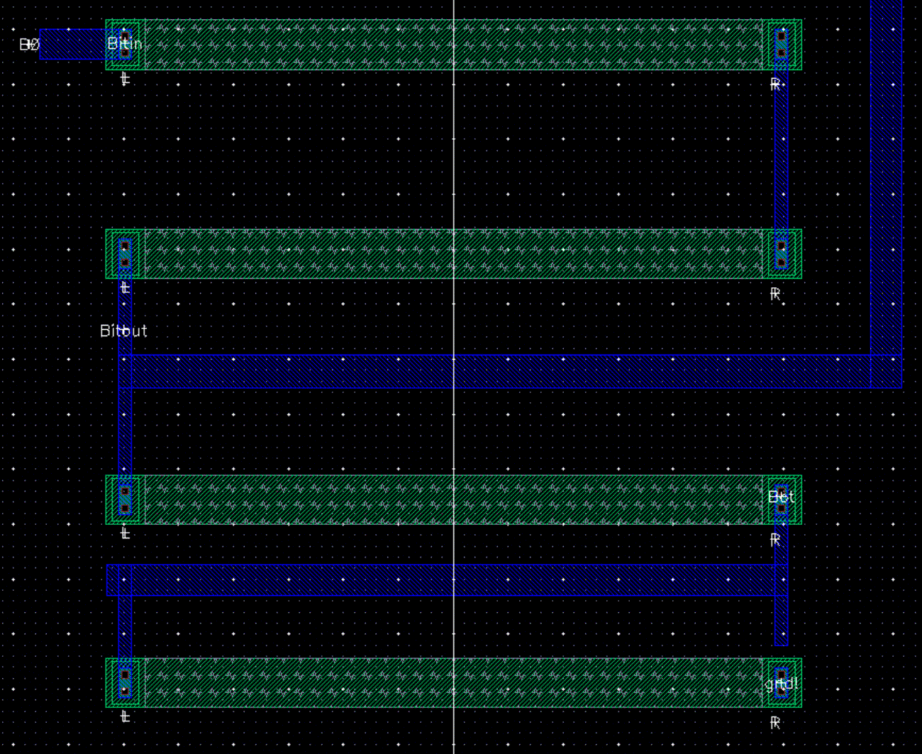
The
complete DAC layout is very large making it very difficult to present
with full details. Below is a picture of the complete DAC layout.
the image is put on its side for formatting.
PROOF!
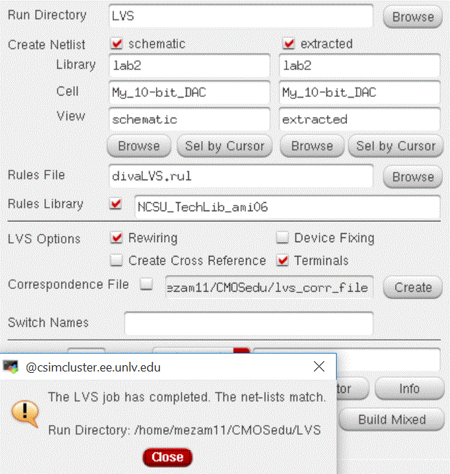
LVS of complete DAC!
|
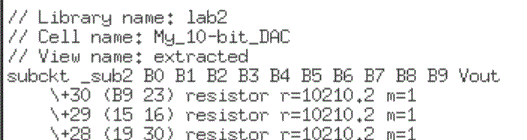
Proof of simulation derived from extracted!
|
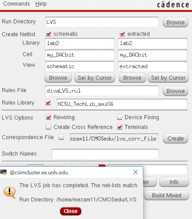
LVS of DAC bit!
|
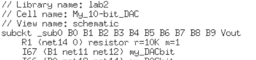
Proof of simulation derived from schematic!
|
Simulation!
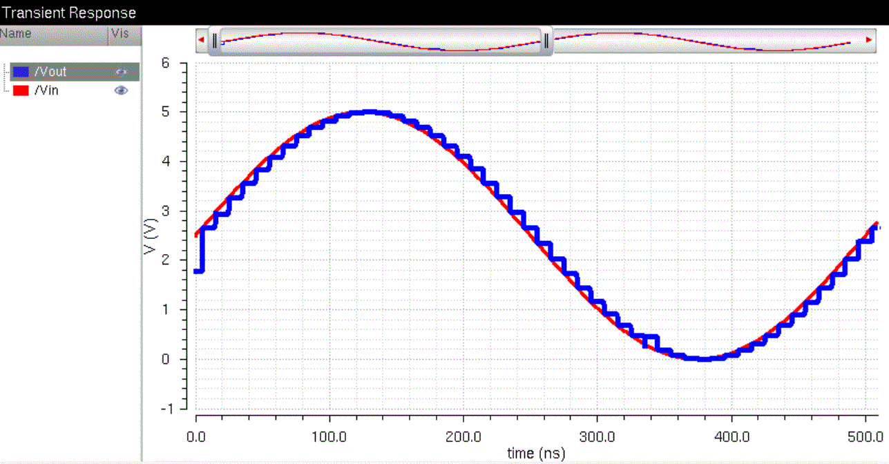
Extracted Simulation of the DAC with no load
|
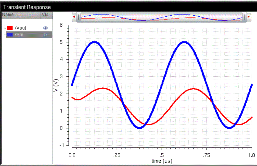
Extracted Simulation of the DAC with an RC load
|
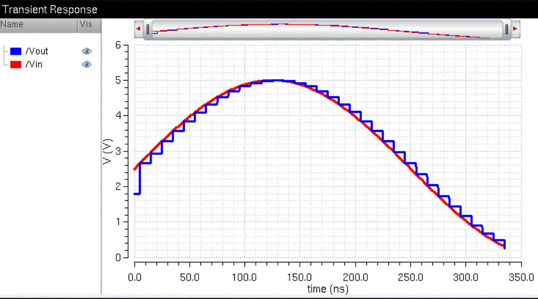
Schematic Simulation of the DAC with no load
|
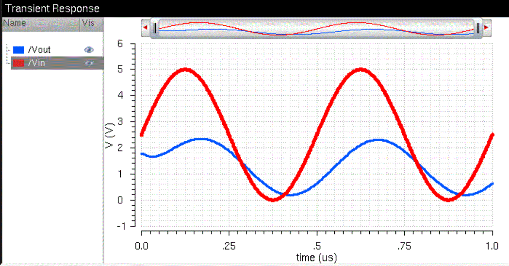
Schematic Simulation of the DAC with an RC load
|
DOWNLOAD CADENCE FILES
Return
to EE 421 Labs