Lab 2 - EE 421L
Digital Integrated Circuit Design
Author:
Matthew Meza
Email:
mezam11@unlv.nevada.edu
August
31, 2015
Design
of a 10-Bit digital-to-analog converter (DAC)
Pre-lab work
- Back-up
all of your work from
the lab and the course.
- Read
through this entire lab
write-up before doing the pre-lab
- Download lab2.zip to your desktop.
- This
archive contains a
simulation example using an ideal 10-bit Analog-to-Digital
Converter (ADC) and Digital-to-Analog Converter (DAC).
- Upload
this zip file to the
design directory on the server that you are running Cadence from, e.g.,
Tutorial_1, CMOSedu, etc.
- Note
that it's assumed you are
using the NCSU Cadence Design Kits.
- Unzip
this directory and add, to
your cds.lib in the design directory, the following statement (assuming
the design directory is CMOSedu):
- DEFINE
lab2 $HOME/CMOSedu/lab2
- Start
Cadence from the
design directory.
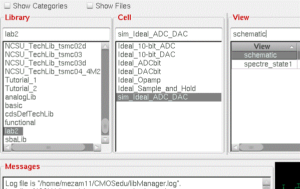
- Use
the Library Manager and
navigate to the lab2 Library as seen below.
- Open
the schematic view of the
cell sim_Ideal_ADC_DAC.
- This
cell contains the ideal
10-bit ADC and DAC.
- Run
the simulation (Launch the
ADE, Session -> Load State -> Cellview -> OK, press the green
start button) to get the following.
- Make
sure you understand how to
change the background color, line thickness, and type of line (e.g.
solid, dashed, etc.)
- Prior
to coming to lab make sure
you understand how the input voltage, Vin, is related to B[9:0] and Vout
(the quiz may ask a question about this).
- In
your lab report: 1) provide
narrative of the steps seen above, 2) provide, and discuss, simulation
results different from the above to illustrate your understanding of
the ADC and DAC, 3) explain how you determine the least significant bit
(LSB, the minumum voltage
change on the ADC's input to see a change in the digital code B[9:0])
of the converter. Use simulations to support your understanding.
- Backup
your webpages and design diretory.
Lab Description
In
this lab we'll use n-well resistors to implement a 10-bit DAC.
Our
design is based upon the topology seen in Fig. 30.14, below, in
the CMOS book.
The
controlling input bits seen below come from the ADC, in other words the
inputs to the DAC are the left side of the 2R resistors.
Lab Requirements
- The
design of a 10-bit DAC using
an n-well R of 10k
- The 2R resistor should be
implement with two separate 10k resistors in series
- After
you've designed and
drafted your schematic check and save it
- How
to determine the output
resistance of the DAC (answer: R)
by combining resistors in parallel and series
- Delay,
driving a load
- Ground
all DAC inputs except B9.
Connect B9 to a pulse source (0 to VDD) and show, and predict using
0.7RC, the delay the
DAC has driving a 10 pF load
- Verify
the simulation results
match your hand calculations
- How
to create a symbol view for
your design with the exact same footprint as the Ideal_10-bit_DAC
symbol view (hint: use
Copy before you start drafting your
design, e.g. Copy the cell Ideal_10-bit_DAC to Mydesign_10-bit_DAC and
then simply edit the schematic view!)
- See Tutorial 1 for additional help
- Note
that your design won't use
VDD, Verfp, or Vrefm so you can delete those pins on your design's DAC
symbol view
- Simulations
to verify your
design functions correctly.
- Copy
the schematic cell view sim_Ideal_ADC_DAC to a cell sim2_Ideal_ADC_DAC and replace the
ideal DAC with the one
you just designed
- Use
the sim2_Ideal_ADC_DAC to
illustrate that your design works as expected.
- Show
what happens if the DAC you
designed drives a load (both R, C, and R/C)
- Explain
what happens if the DAC
drives a 10k load?
- In a
real circuit the switches seen
above (the outputs of
the ADC) are implemented with transistors (MOSFETs).
- Discuss
what happens if the
resistance of the switches isn't small compared to R.
Pre-Lab
Excercise
1) provide
narrative of the steps seen above:
2) Provide, and discuss, simulation
results different from the above to illustrate your understanding of
the ADC and DAC
3) explain how you determine the least
significant bit
(LSB, the minumum voltage
change on the ADC's input to see a change in the digital code B[9:0])
of the converter.
All
three are provided below!
After unzipping
the folder provided, open the "sim_Ideal_ADC_DAC" schematic cell view.
Changing the folder name of the zipped file can cause complications so
use the default name for simplicity!
|
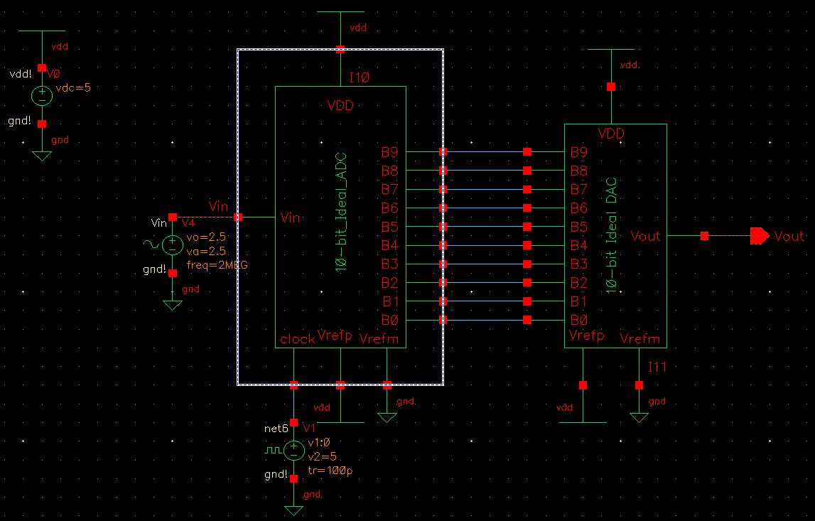
The following
schematic will show! The voltage source
on the left may be changed to
observe changes in the DAC!
|
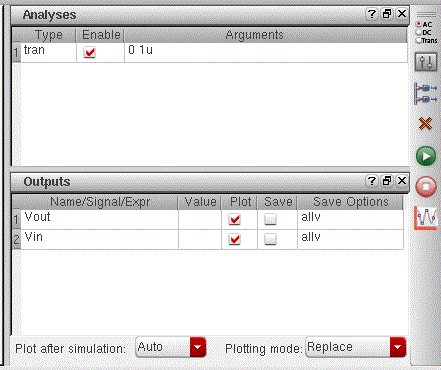
After changing
the voltage source, click on the top left and choose the ADE option!
After opening the save state provided, the ADE window should look like
above !it is important to make sure that the simulation time matches
with the plot time length. If not then we must follow the provided
steps to force the simulation to converge. This is shown below.
|
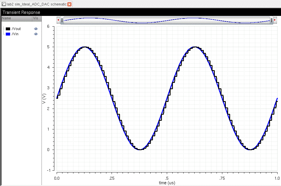
When looking at
the input/output notice the zero-order hold quality of the output. We
can see that the output has a "step" quality. In our situation this
"step" is due to the clock of the ADC, NOT the DAC. To determine the
LSB of the DAC we can use the following equation:
LSB = VDD/(2^n) where n is the
number of bits!
This can be seen again below
in the Post-Lab excercise!
|
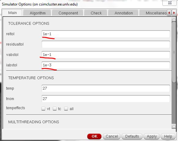
- If
you have simulation convergence problems you can force the simulation to converge
by going to, in the ADE, Simulation -> Options -> Analog
- Set
the values as seen below
- relative
tolerance, reltol, of 10% (= 1e-1)
- voltage
absolute tolerance, vabstol, of 100 mV (= 1e-1)
- current
absolute tolerance, iabstol, of 1 mA (= 1e-3)
- The
accuracy of the simulation will, obviously, be degraded
Post-Lab Excercises
The design of a 10-bit DAC
using
an n-well R of 10k
The 2R resistor
should be
implement with two separate 10k resistors in series
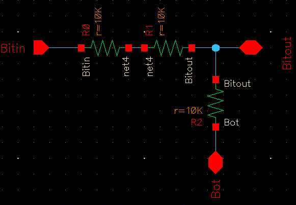
Above is the my DAC Bit. A symobl of this schematic is used
in the next picture to create the complete DAC. This design
allows me to change the number of bits in the DAC on the fly
for future projects!
|
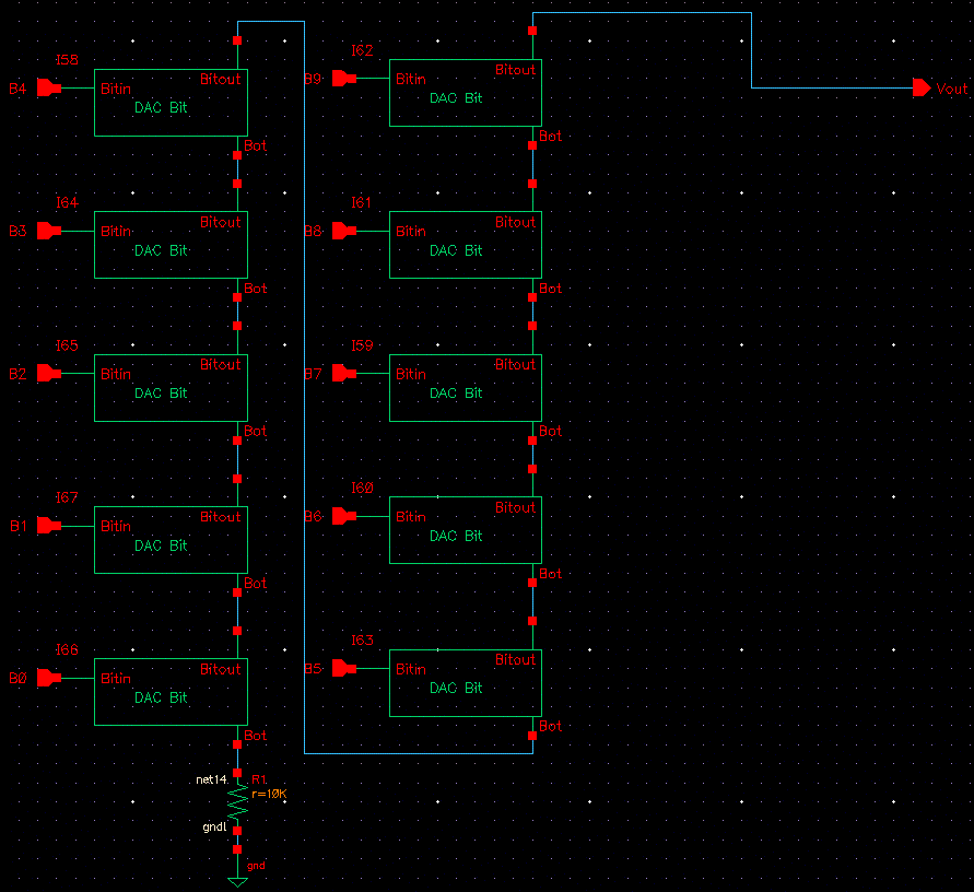
Shown is schematic of my DAC using a symbol created
from the circuit shown to the left. Notice how I stacked
each bit ontop of one another. Also notice that I placed
a resistor at the bottom of the bit.
|
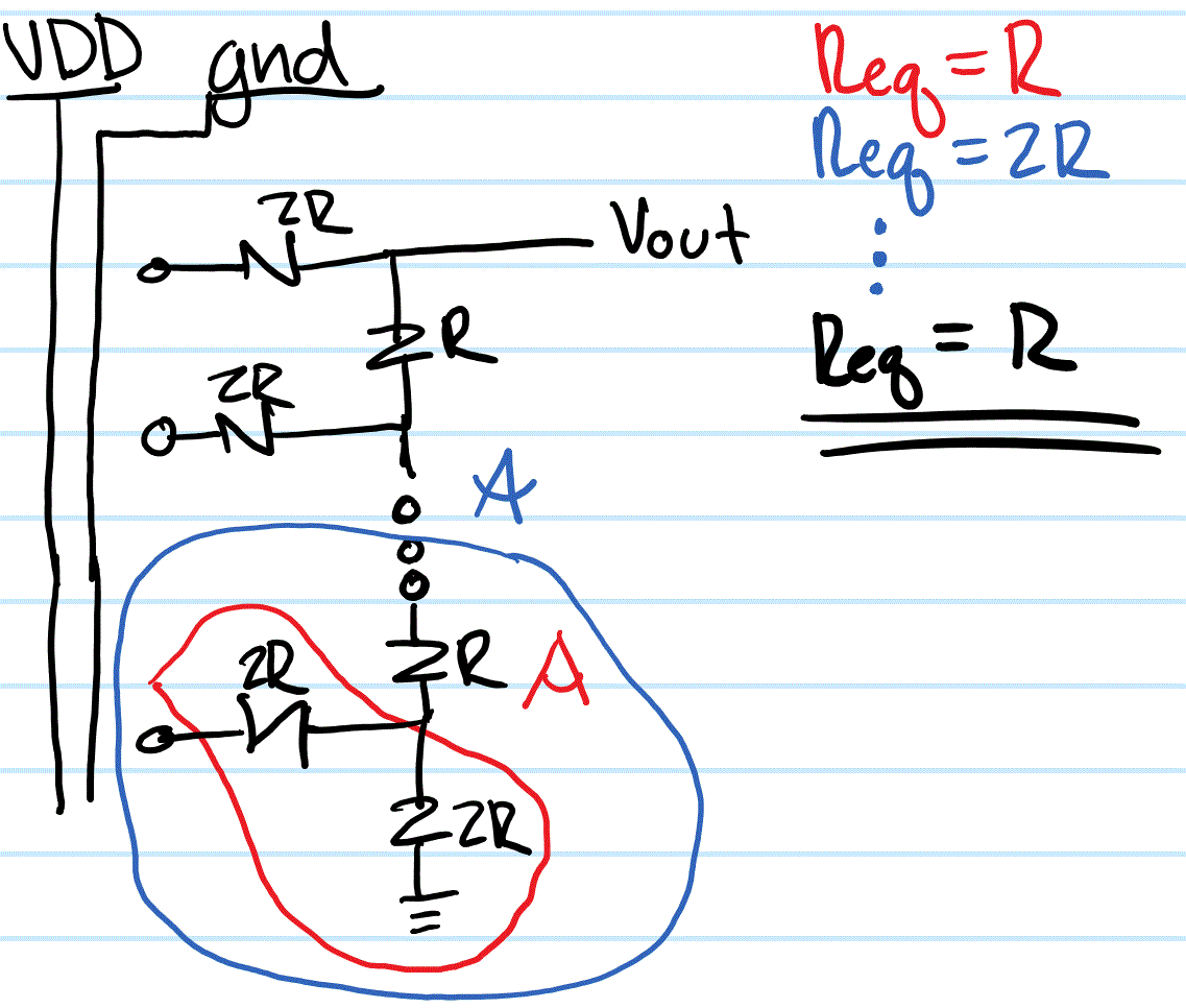
How to determine the output
resistance of the DAC. Solution shown in black!

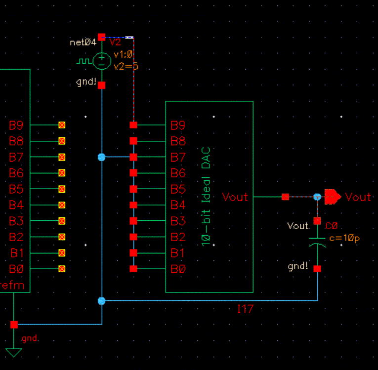
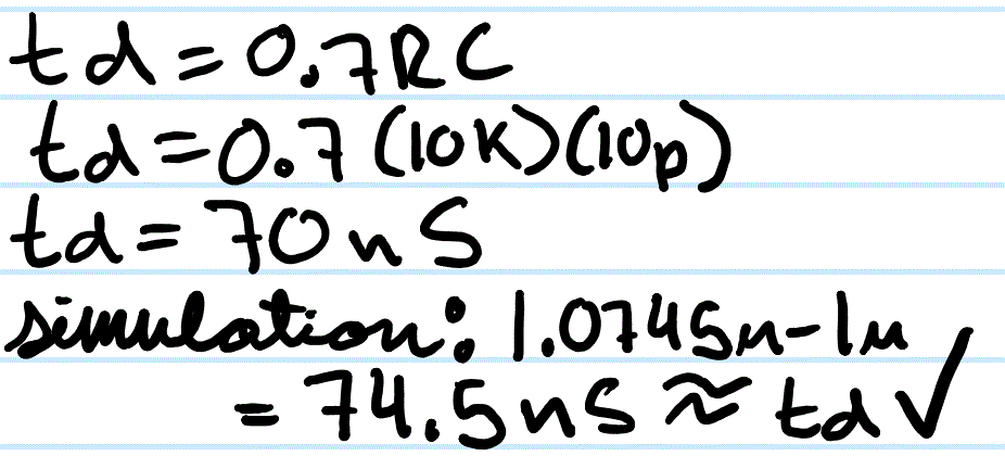
Delay, driving a load: Ground all
DAC inputs except B9.
Connect B9 to a pulse source (0 to VDD) and show, and predict using
0.7RC, the delay the DAC has driving a 10 pF load. Verify
the simulation results
match your hand calculations.
Schematic of (My
designed) DAC driving a 10p load
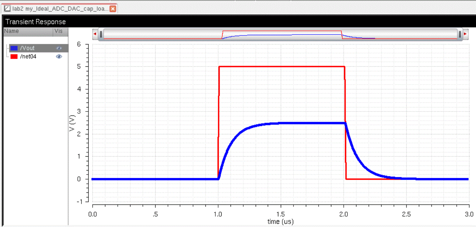
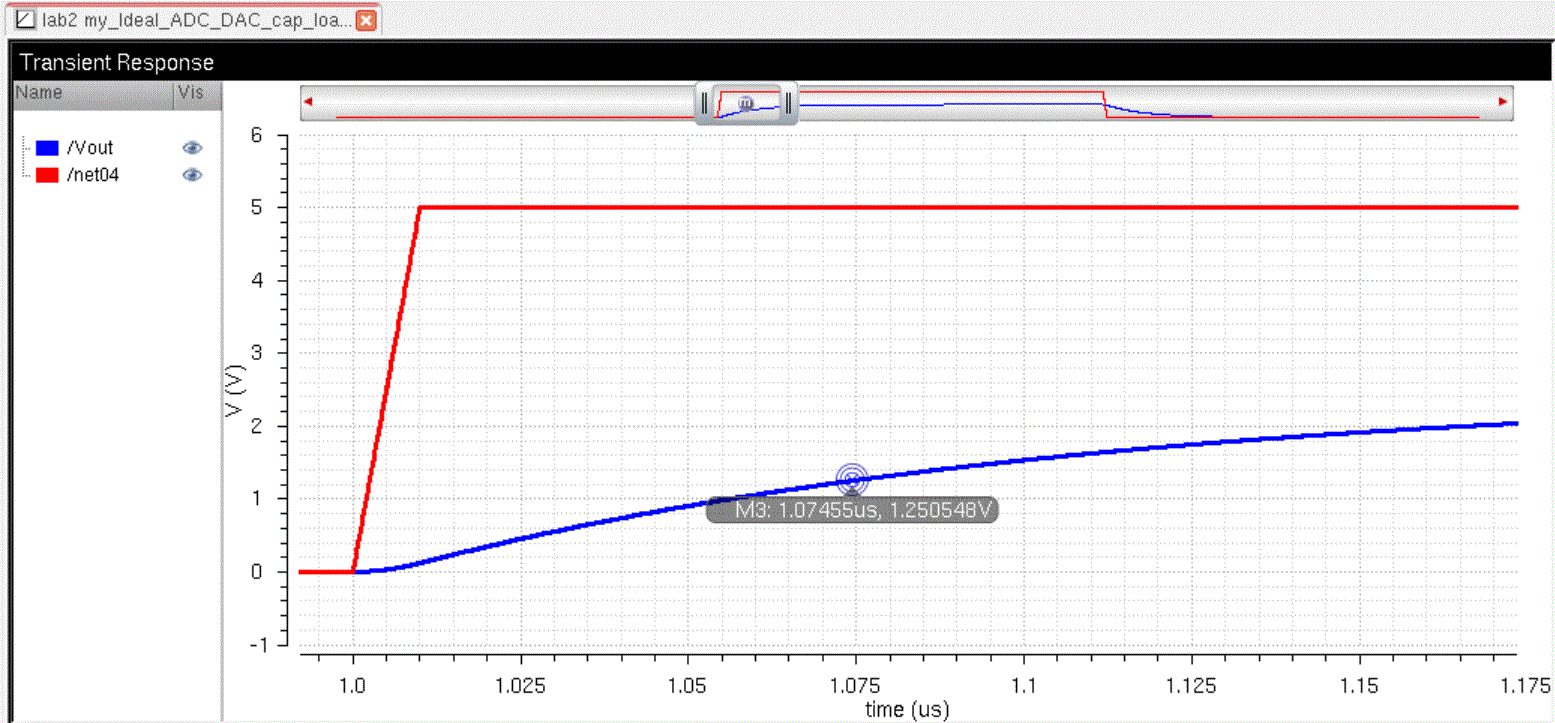
Simulation and Hand Calc
of time delay!
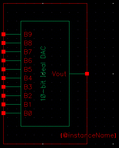
How to create a symbol view for
your design with the exact same footprint as the Ideal_10-bit_DAC
symbol view (hint: use
Copy
before you start drafting your
design, e.g. Copy the cell Ideal_10-bit_DAC to Mydesign_10-bit_DAC and
then simply edit the schematic view!)
My DAC Design!
DAC
design implemented into a symbol!
Show what
happens if the DAC you
designed drives a load (both R, C, and R/C)
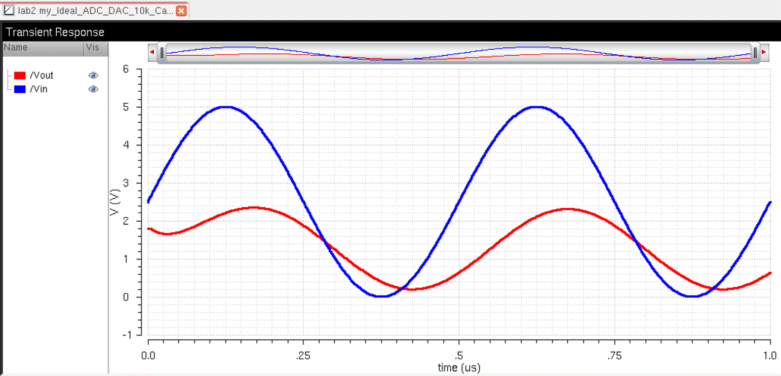
DAC driving
a 10K resistor
Notice the loss in amplitude/gain!
|
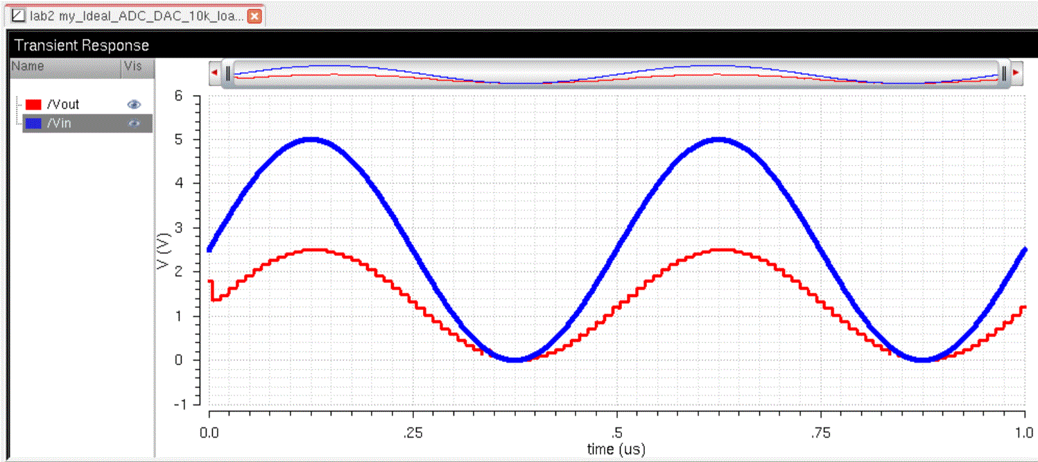
DAC Driving a
10K resistor and 10p Capacitor
Notice the loss in amplitude/gain and a phase shift!
|
DAC driving
a 10p Capacitor
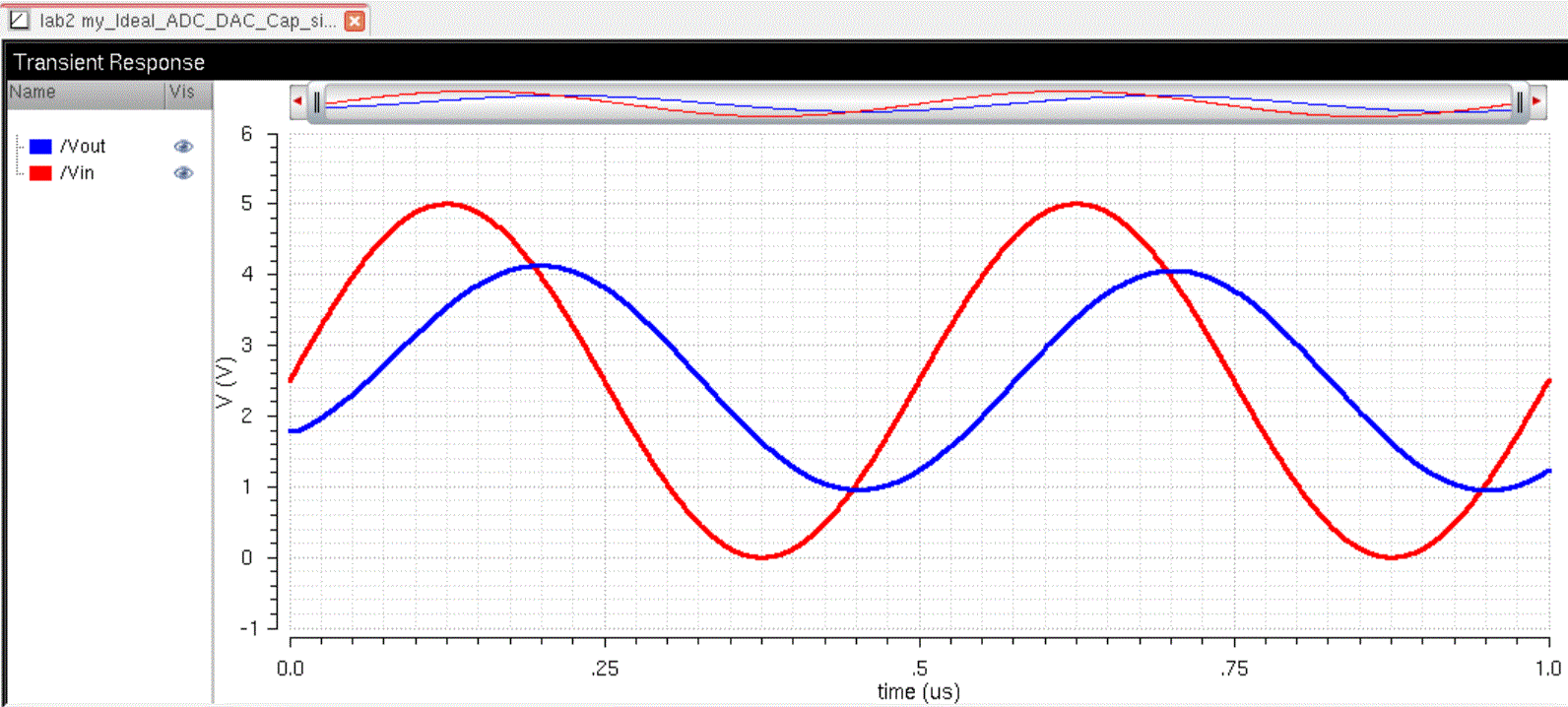
notice the phase shift and loss in magnitude!
|
General
Schematic!
|
Explain what happens if the DAC
drives a 10k load?
As shown above, driving a 10K
resistor will result in a voltage divider efffect! There will be a loss
in gain and the maximum value of
the DAC will be approximately half of VDD!
In a real circuit the switches seen above (the outputs of
the ADC) are implemented with transistors (MOSFETs).
Discuss
what happens if the
resistance of the switches isn't small compared to R.
Shown below is an example of a MOSFET being
used as a switch as the output of an ADC!
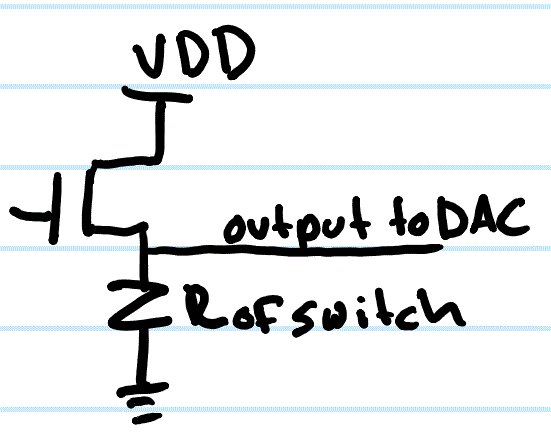
If the resistance of
the switch (R of switch) is large
compared to R of the DAC then the switch input
resistor of 2R will actually be larger which will
affect the perfomance of the DAC!
Return
to EE 421 Labs