Lab 3 - ECE 421L
See the EE421L webpage here
Authored by Juan Buendia
buendiaj@unlv.nevada.edu
September 20, 2015
Objective: Layout of a 10-bit digital-to-analog converter (DAC)
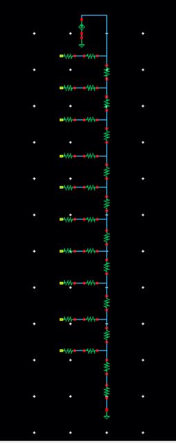
The circuit will be based on the following DAC schematic, but will use nwell resistors.
The equivalent resistance is R given by the following.
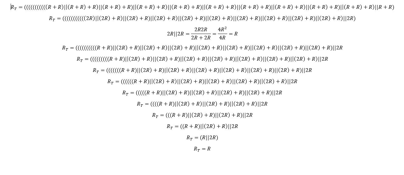
The least significant bit is about 4.88 mV.
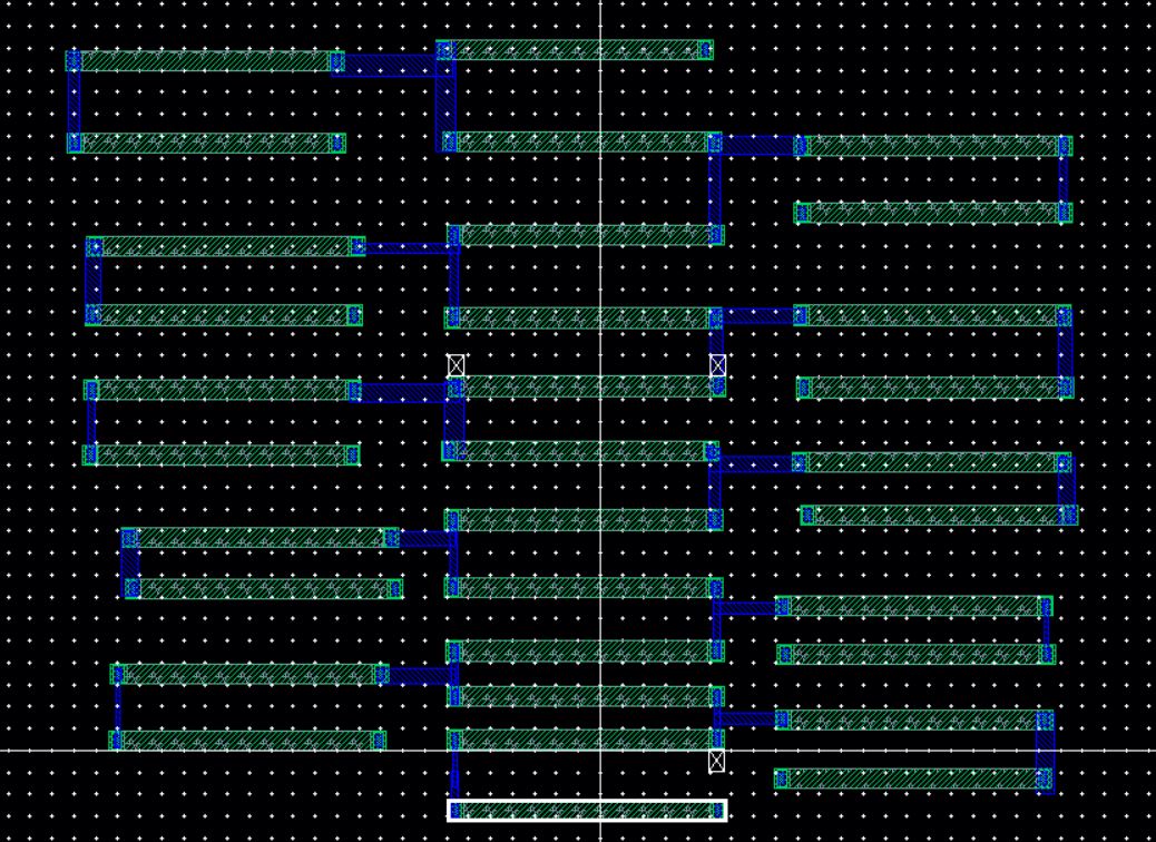
The layout
The final step is to back the lab 3 file
Return to buendiaj's labs
Return to EE421L Labs