See the EE421L webpage here
Authored by Juan Buendia
buendiaj@unlv.nevada.edu
August 30, 2015
Objective - Design of a 10-bit digital-to-analog converter (DAC)
Prelab - Understand how an analog to digital (ADC) and a digital to analog (DAC) work
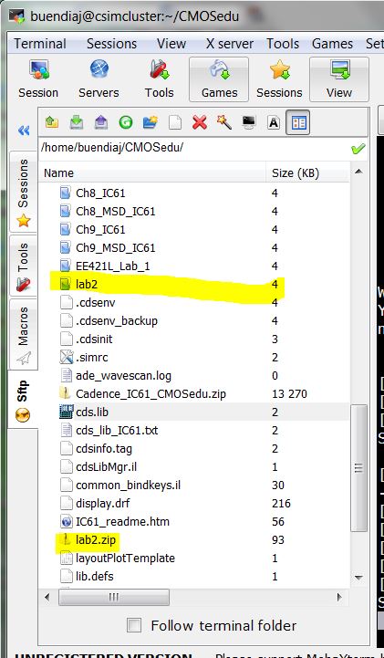
We downloaded the lab2 zip file and extracted it onto our CMOSedu directory on Mobaxterm.

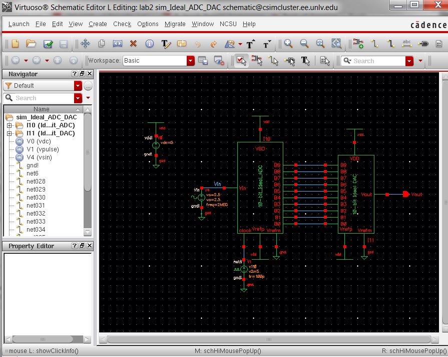
After running Cacence, we opened an ideal ADC and DAC (sim_ideal-ADC_DAC) from the lab2 library in the library manager.
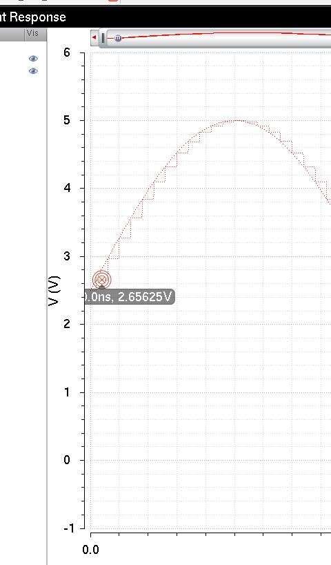
We ran a simulation using spectre from the ADE L menu and got the following result:
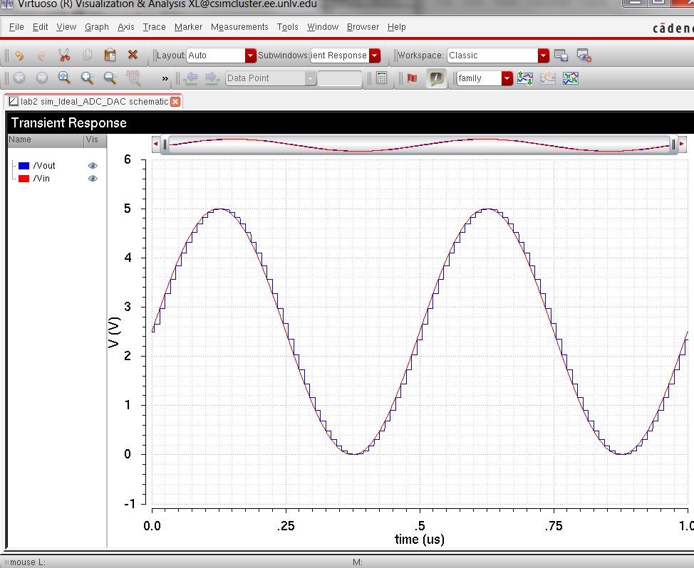
The period of the the sample clock is 10ns.
This corresponds to 1/50 of the period of the input (the period is 500ns).
Each clock inpulse samples when the input changes in phase by 7.2 degrees.
Therefore, each bit changes every time the input changes in phase by 7.2 degrees.
If we use the formula,