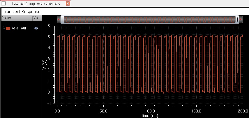
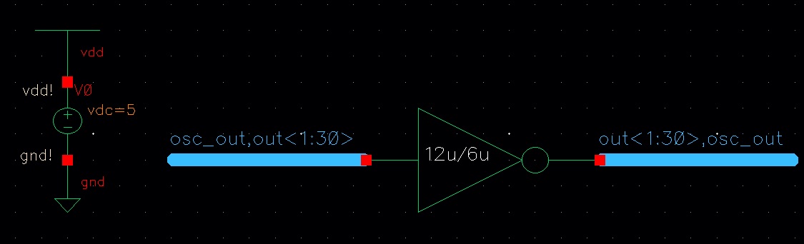
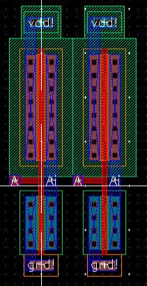
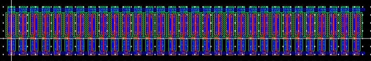
This lab will go over using buses and arrays in the design of word inverters, muxes, and high-speed adders. The lab begins with completing Tutorial 5 seen here. Seen below are some of the images from the completion of Tutorial 5.
We will first begin by designing and simulating a 4-bit inverter.
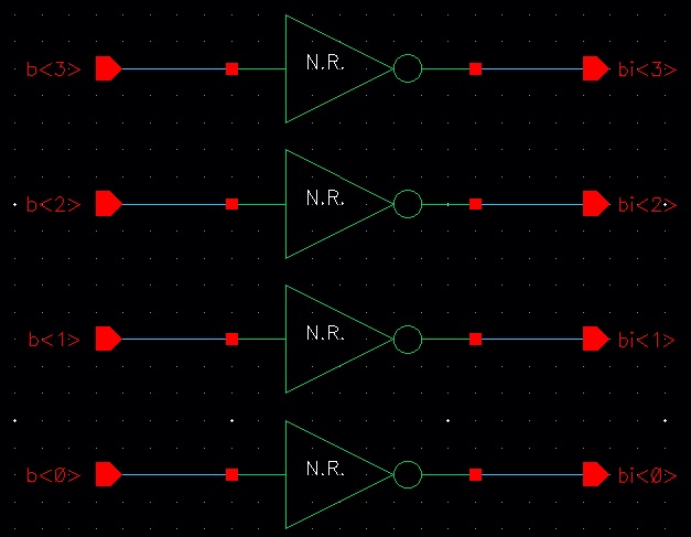
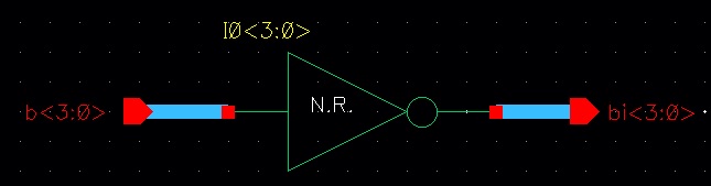
We can make a cleaner schematic using buses and arrays, as seen below:
Schematic:
Symbol:

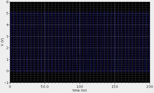
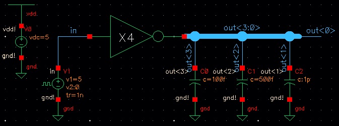
Next we will simulate the 4-bit inverter. The simulation schematic is seen below:
Below is the result of the simulation. It is clear that the inverter is working properly:

As you can see above, the higher the Capacitive Load, the longer the rise and fall times of the inverter are.
The next task of this lab is to create schematics and symbols for an 8-bit input/output array of: NAND, NOR, AND, inverter, and OR gates. We have designed the NAND Gate and Inverter in previous labs, but the new schematics and symbols are found below:
AND2 - Schematic

AND2 - Symbol

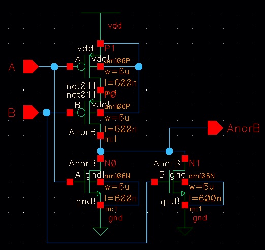
NOR2 - Schematic
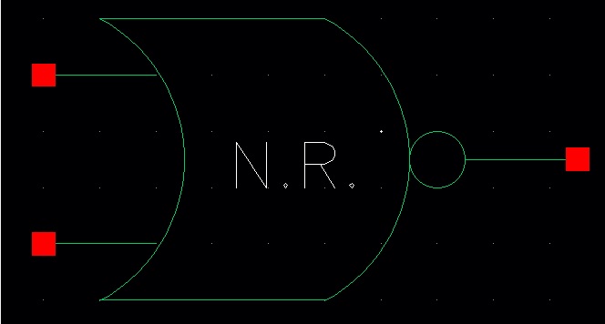
NOR2 - Symbol
OR2 - Schematic

OR2 - Symbol

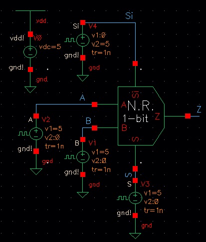
Now it is time to simulate that the gates are working properly. We begin by designing the schematic and symbol for the simulation of the gates for 1-bit:
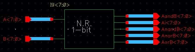
Gates (1-bit) - Schematic

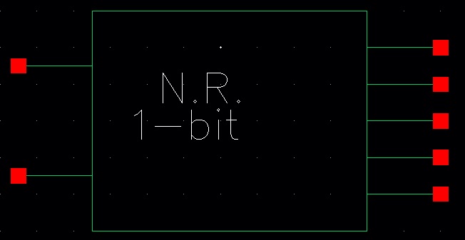
Gates (1-bit) - Symbol
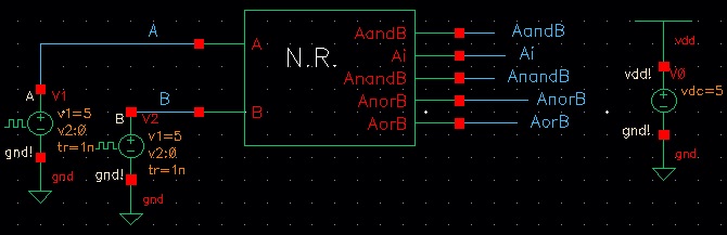
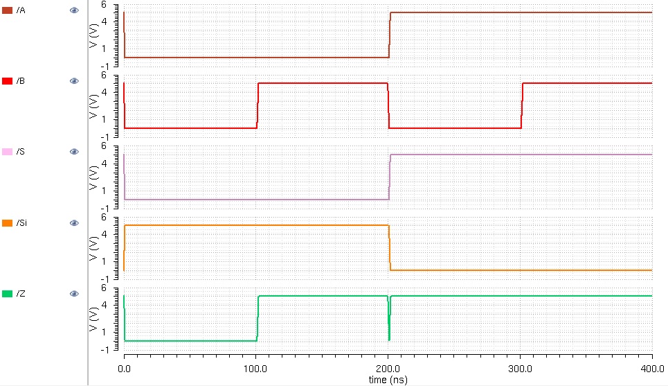
Using the symbol, we can draft a schematic for simulating the 1-bit gates
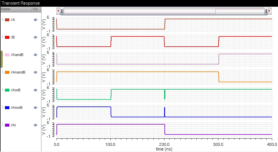
The simulation results are seen below. It is clear that all of the gates are working properly.
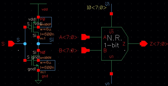
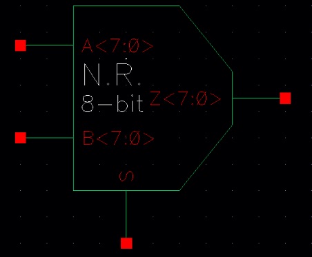
Now that we know the gates are working properly, we can design the 8-bit version of the gates. The resulting schematic and symbol are seen below:
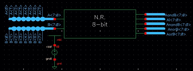
Gates (8-bit) - Schematic
Gates (8-bit) - Symbol

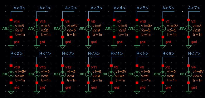
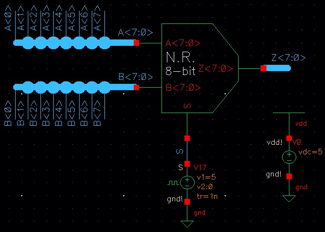
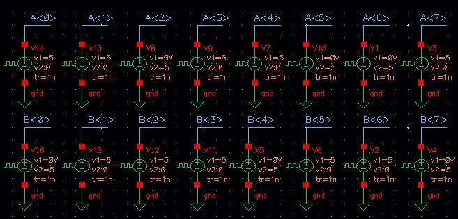
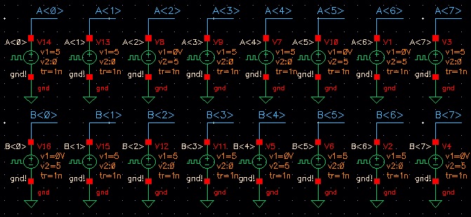
Now it is time to simulate the 8-bit version of the gates. The schematic is quite large because I wanted to give different values for each bit of the input (A/B). The schematic is seen below:
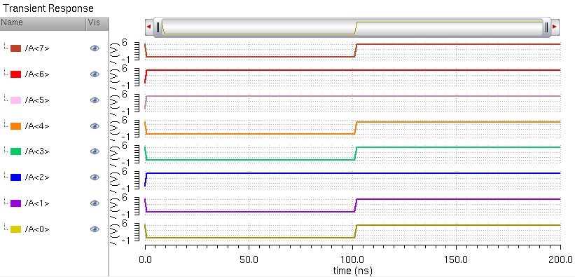
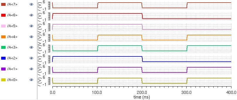
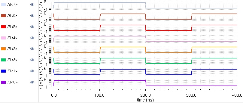
The results of the simulation can be seen below:


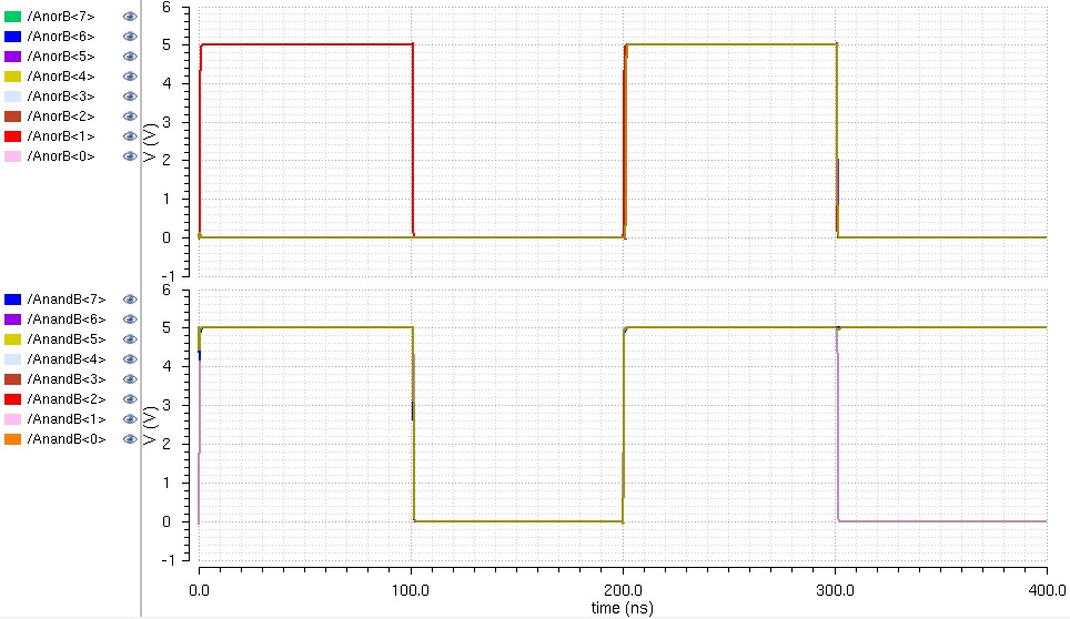
The results may be hard to read because there are so many bits. For a better breakdown, you can view the complete simulation found in the zip file at the end of the lab.
The next part of the lab is to design and simulate an 8-bit 2-to-1 DEMUX/MUX. We will begin with a 1-bit DEMUX/MUX to verify that it works. Below is the schematic and symbol for it:
2-to-1 DEMUX/MUX (1-bit) - Schematic

2-to-1 DEMUX/MUX (1-bit) - Symbol

Next we will simulate the 1-bit DEMUX/MUX. The schematic and simulation results can be seen below:
Now that the 1-bit version works, it's time to make the 8-bit schematic and symbol.
Now it is time to simulate. The schematic can be seen below. I set the power supplies individually so I could control each one. To save space, I split the image into two parts, as seen below.
Ok let's simulate to verify that it is working.
A:
B:
S:

Z:

As expected, when the select is low, B is selected as the output. Now let's simulate it when the select is high but A & B stay the same.

Now A is getting selected as intended.
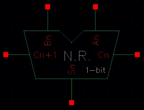
Now it is time to simulate and layout the full adder as seen in Fig. 12.20. Below is the figure. We begin by drafting the schematic and symbol for 1-bit of the adder.

Schematic:

Symbol:
Now it is time to simulate the 1-bit full adder. The simulation schematic and simulation results are seen below.
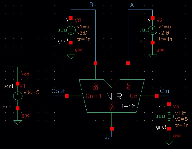
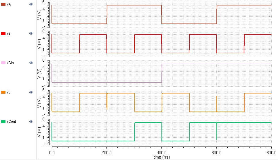
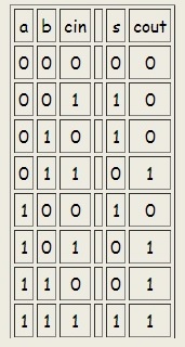
The simulation verifies that the schematic works. The truth table can be seen below for verification.
Now that we know the adder works for 1-bit, it is time to draft the 8-bit full adder. The schematic and symbol can be seen below.
Schematic:
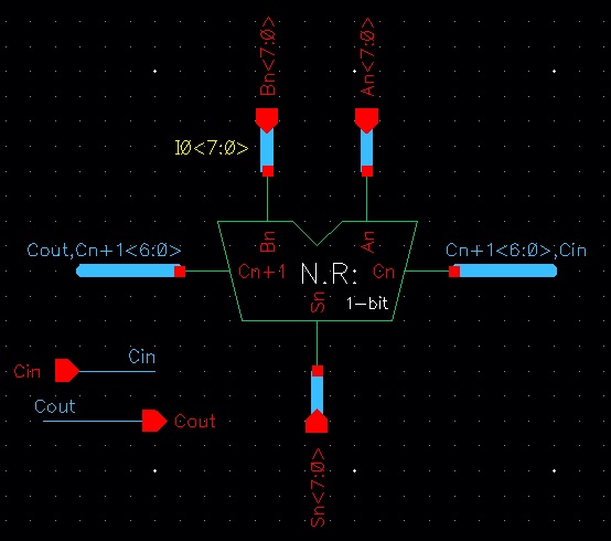
Symbol:

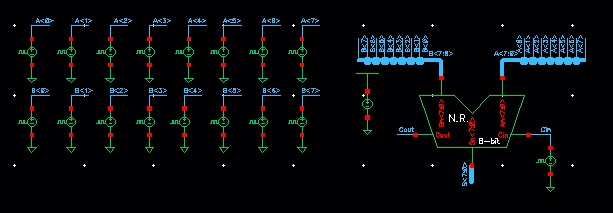
Next it is time to simulate the 8-bit full adder. Like before, I broke the schematic image into multiple parts to save space, they are seen below.

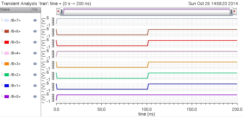
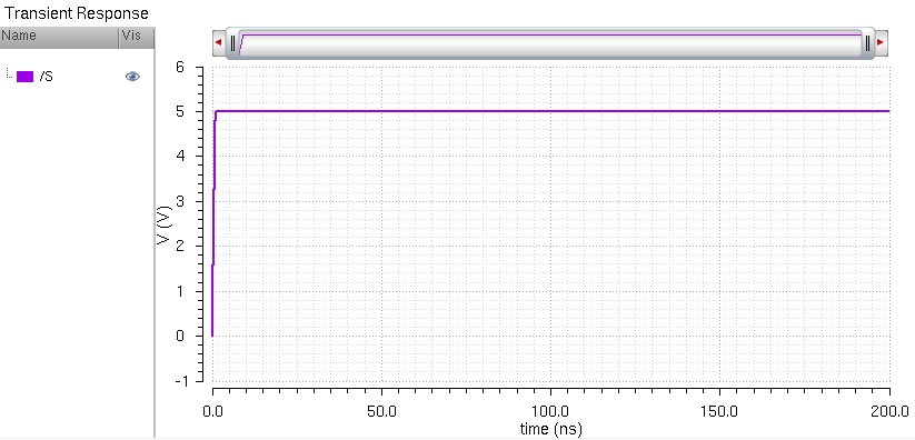
Now it is time to simulate the 8-bit full adder. I ran it for 4 pulses so there are 4 additions being done. The results can be seen below.
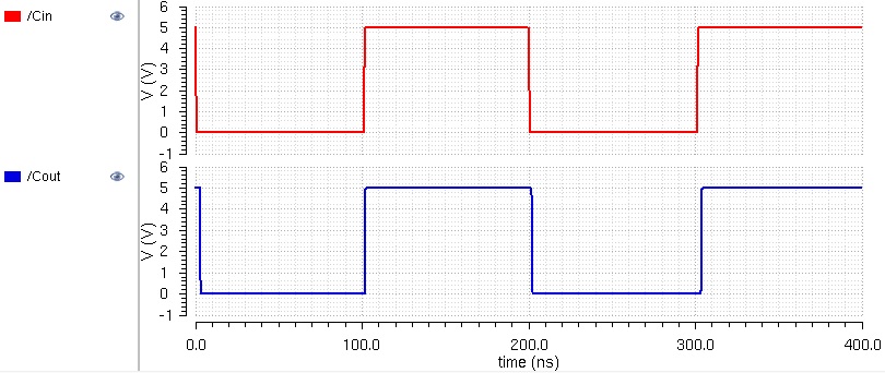

Before we move on, let's analyze the results to make sure that it works properly. To begin, let's look at the first addition
(Time 0-100ns):
A = 01100100 = 100 (in decimal)
B = 10010001 = 145 (in decimal)
Cin = 0
S = 11110101 = 245 (in decimal)
Cout = 0
Let's check one more time fragment to verify it works. Let's look at the last addition.
(Time 300-400ns):
A = 10011011 = 155 (in decimal)
B = 01101110 = 110 (in decimal)
Cin = 1
S = 00001010
Cout = 1
Since we have Cout = 1, we bring the 1 in front of the S, giving us a value of
Sum = 100001010 = 266 (in decimal)
Now that we have verified that the 8-bit schematic works, it is time to do the layout for the cell. Like always, we begin by laying out 1-bit of the cell. The result can be seen below.
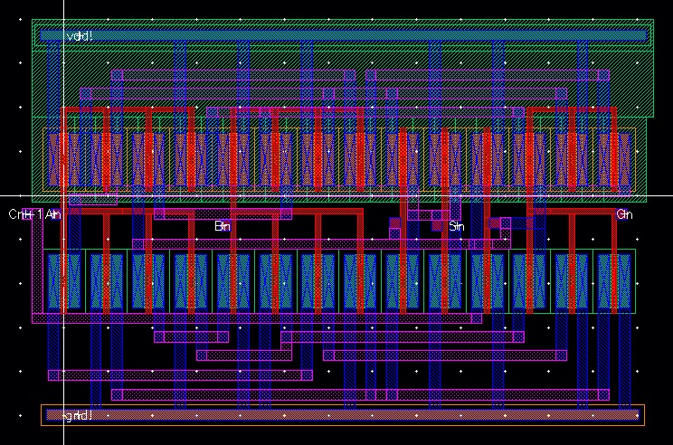
I have placed Cn and Cn+1 on opposite sides of the cell in order to make it easy to link multiple bits of the cell together. This will help us soon.
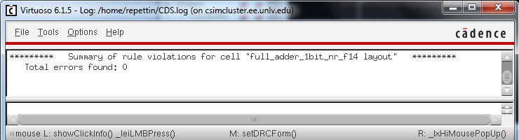
Let's do a DRC and LVS to verify that the 1-bit layout is correct. The results are seen below.

Now comes the fun part. It is finally time to lay out the entire 8-bit full adder. I begin by placing the 1-bit cell down and copying it 7 more times so I have 8 identical 1-bit adders.

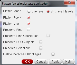
Next I flatten all of the cells in order to connect them together.
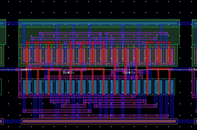
Once the cells are flattened, it's time to start connecting them together and adding the pins. I begin with Bit0, placing pins Cin, S0, A0, B0, and connecting Cout to the next bit's Cin, as well as the vdd! and gnd!.

Next I move onto Bit1, placing pins S1, A1, B1, and connecting Cout to the next bit's Cin, as well as the vdd! and gnd!.
Finally, I continue this trend through all the bits until I get to the last bit. I place pins S7, A7, B7, and Cout.
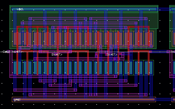
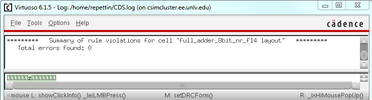
The layout is now complete, let's do a DRC and LVS to make sure it works.
DRC:
LVS:
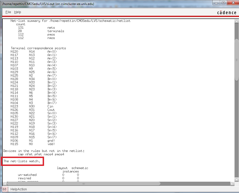
It works!
The lab is now complete. All of the work from this lab can be found in the zip file lab7.zip