This lab will go over the design, simulation and layout of a CMOS NAND gate, XOR gate, and Full Adder. The lab begins with completing Tutorial 4 seen here. Seen below are the images from the completion of Tutorial 4.
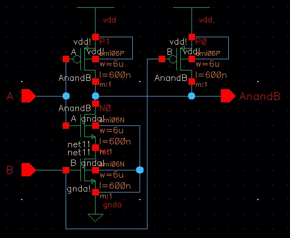
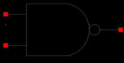
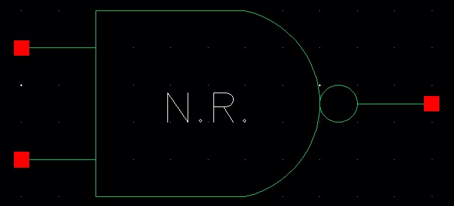
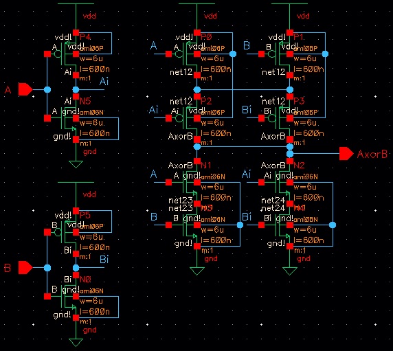
We will first begin by drafting the schematics and symbols of the CMOS NAND gate and XOR gate. The images are seen below.
NAND2

XOR2

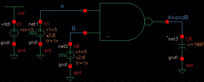
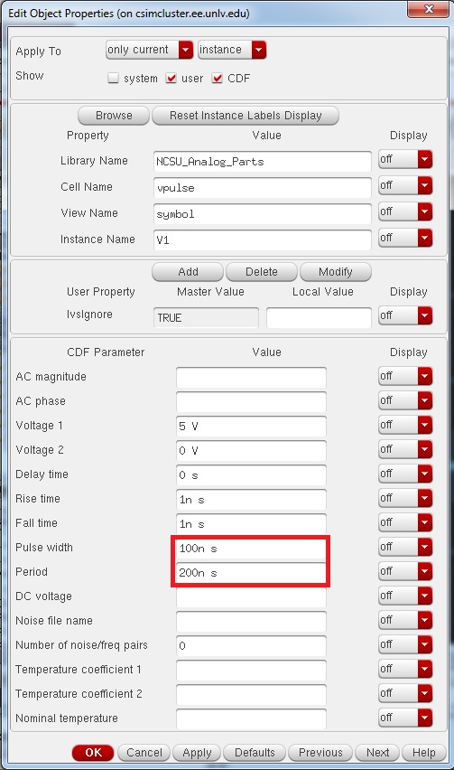
Next we will simulate the gates to verify that they are working correctly. Below is the schematic and pulse properties for the simulation:
Schematic
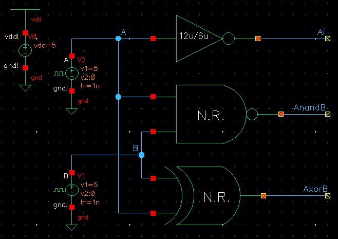
A Pulse
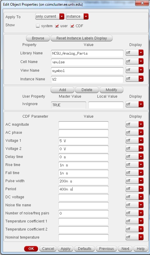
B Pulse
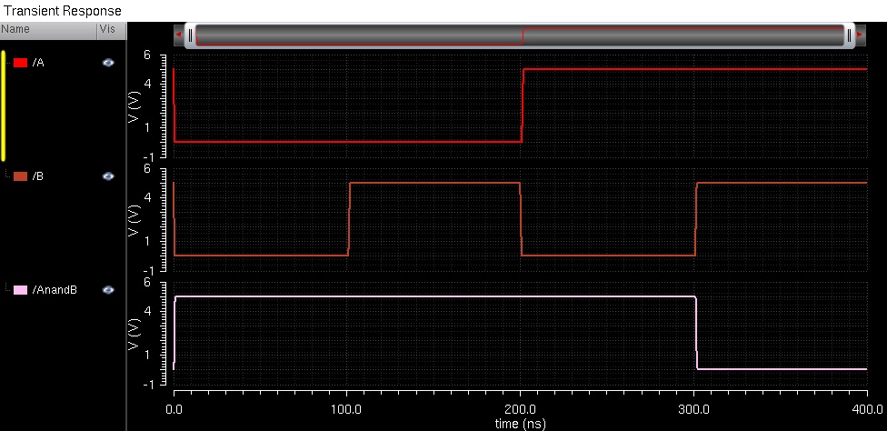
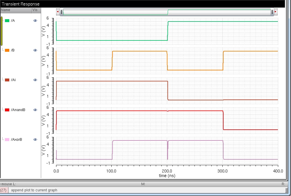
Below is the result of the simulation. It is clear that the gates are working properly:
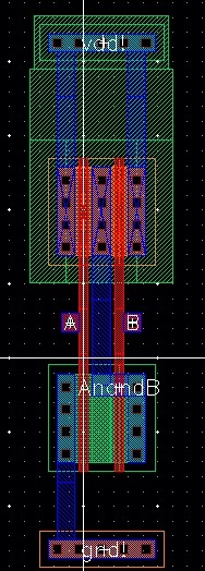
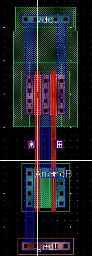
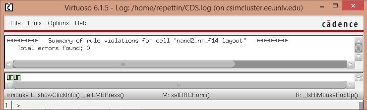
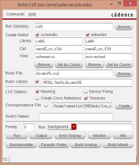
Next we must design the layout for the NAND and XOR gates. We also verify that they meet the Design Rules and we also do an LVS for each. The results are seen below:
NAND2
Layout
DRC Results
LVS Setup
LVS Results

XOR2
Layout
DRC Results
LVS Results

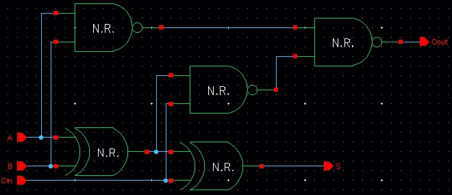
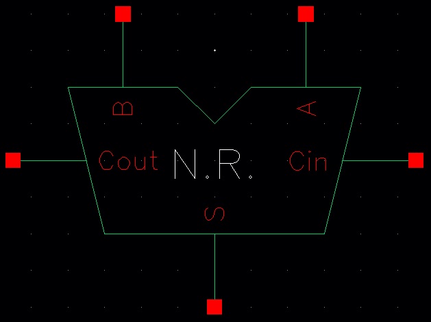
Next we must design the full adder. The schematic and symbol are seen below:
Now it is time to simulate it to verify it works:
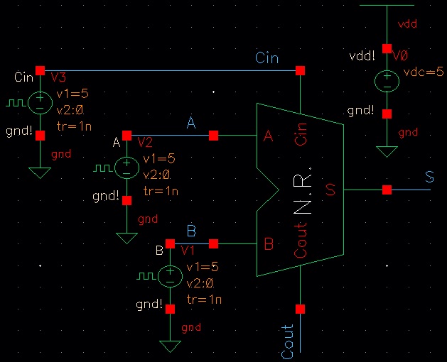
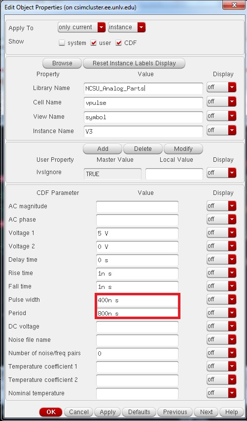
Cin pulse setup. A and B are the same setup as before.
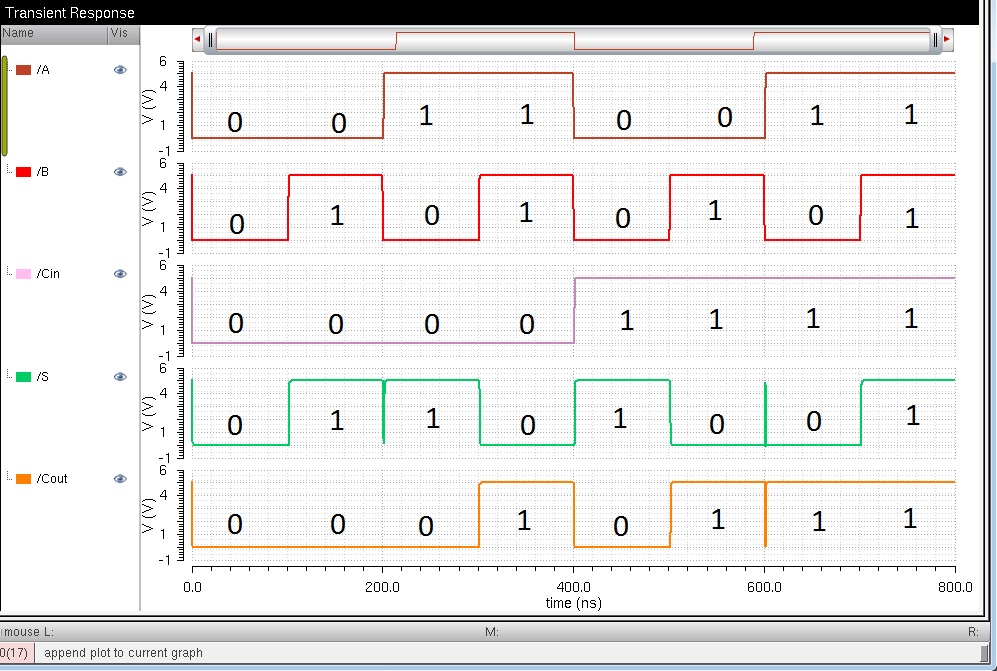
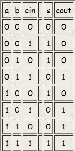
The simulation results are seen below. The match up with the Truth Table (also below):
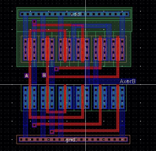
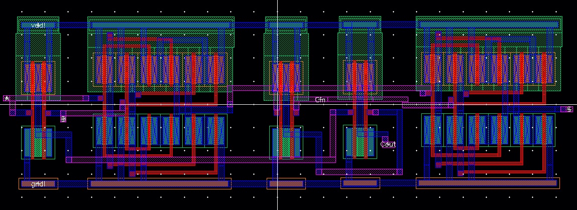
Finally it is time to layout the full adder. The results can be seen below:
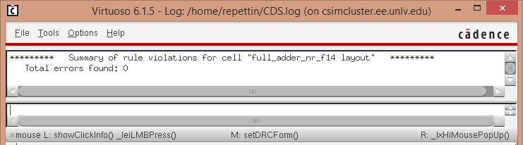
Let's do a DRC to make sure everything checks out ok:
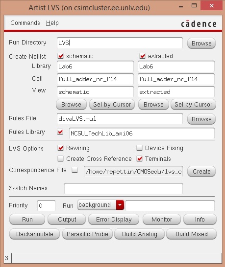
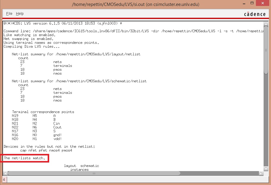
Now lets do a LVS. The setup and results are seen below:

The lab is now complete. All of the work from this lab can be found in the zip file lab6.zip