Lab 5 - EE 421L
Authored by Nick Repetti
repettin@unlv.nevada.edu
10/13/2014
Lab Description:
This lab will go over the design, simulation and layout of a CMOS Inverter. The lab begins with completing Tutorial 3 seen here.
Lab Report:
This lab requires us to draft the schematics, symbols, layouts, and simulations for 2 inverters having sizes of:
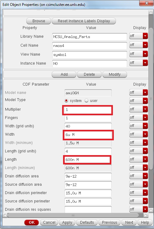
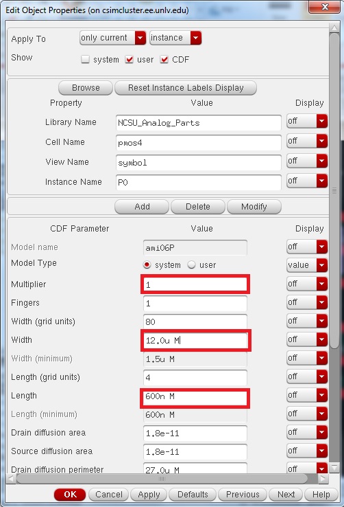
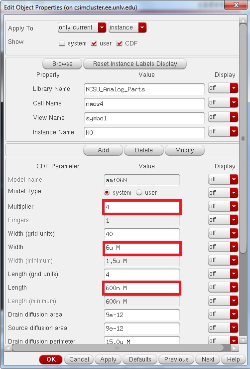
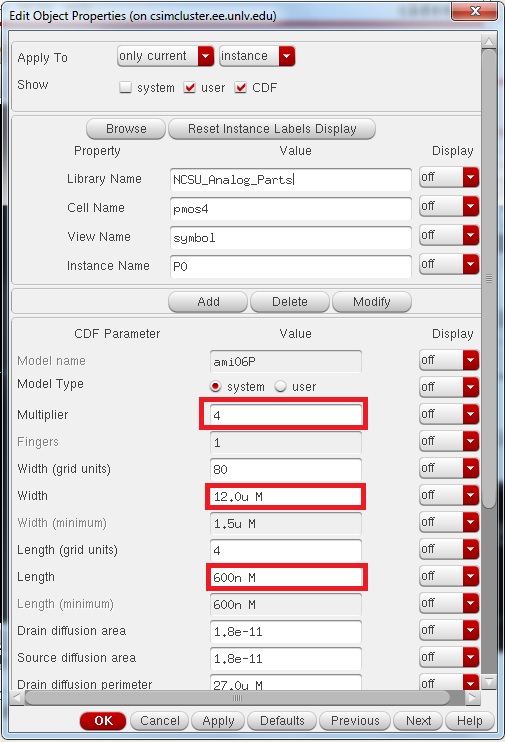
We will start with the schematic for the first inverter. Seen below are the properties for the NMOS and PMOS devices we will be using.
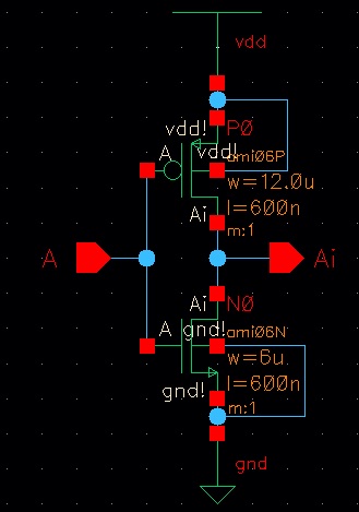
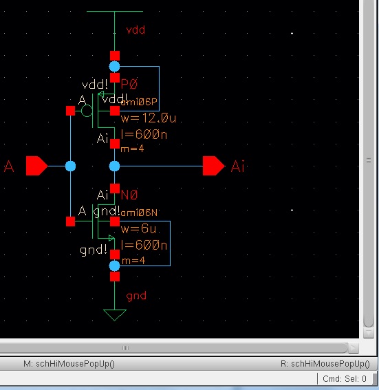
Below is the schematic for the first inverter:
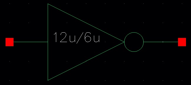
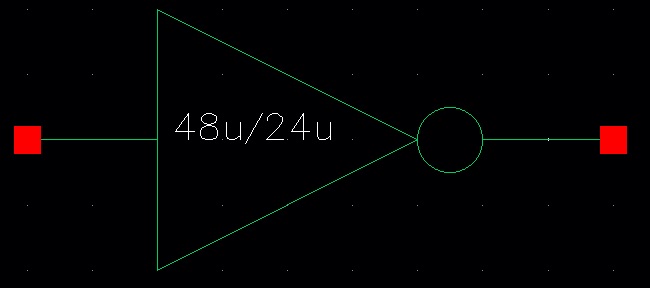
Next we draft the symbol as we have done in previous labs:
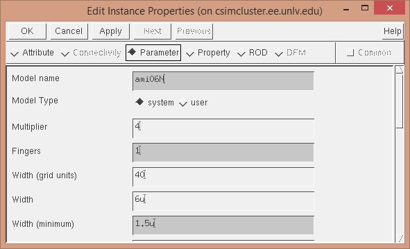
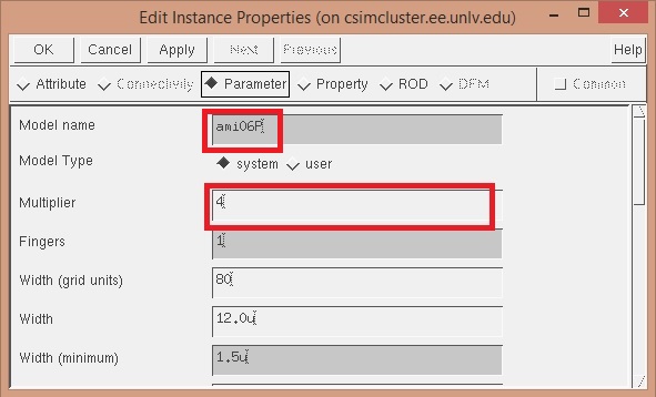
Next we will draft the schematic for the second inverter. Seen below are the properties for the NMOS and PMOS devices:
The resulting schematic can be seen below:
Like before, we draft a corresponding symbol for the schematic:
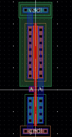
Next we will do the layout for the first inverter. We begin by placing a pmos and an nmos:
Using ntap, ptap, m1_poly, and the poly and M1 layers, we can create the layout for the first inverter. We also add pins on the M1 layer.
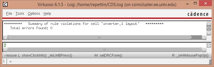
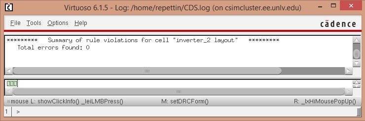
Next we DRC the layout to make sure all rules are being followed.
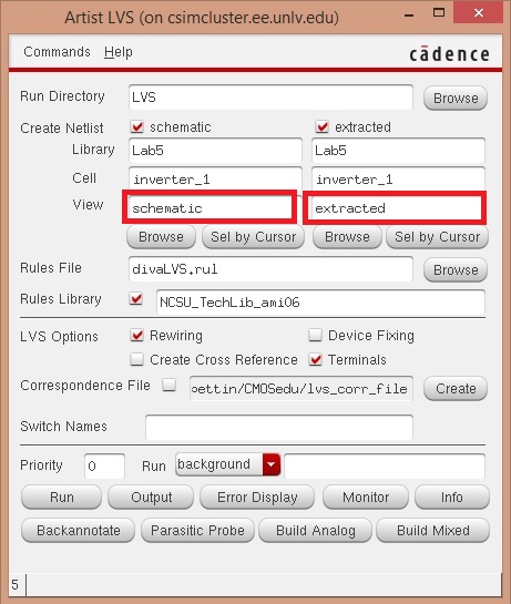
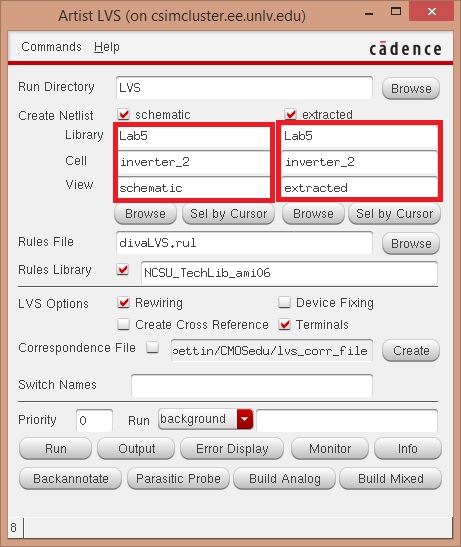
Finally it is time to LVS the layout. The setup and results are seen below:

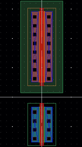
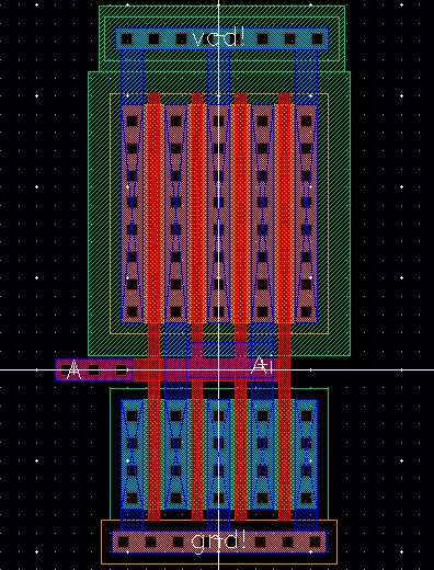
Now it's time to do the layout for the second inverter. We begin by placing nmos and pmos, after configuring their multiplier as seen below:
Next we draft the layout just like we did before with the first inverter.
Let's do a DRC to make sure everything checks out ok:
Now lets do a LVS. The setup and results are seen below:

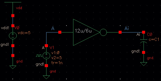
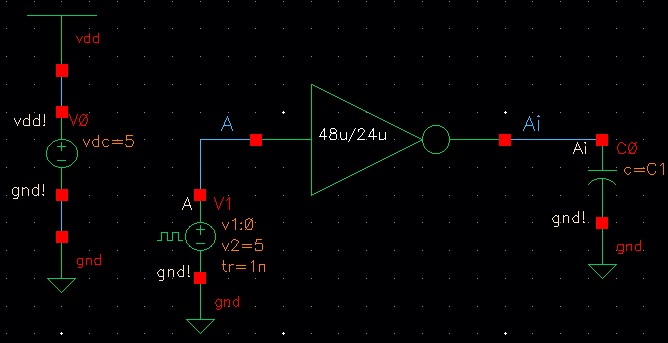
The next part of the lab is to simulate each inverter with a capacitive load of 100f, 1p, 10p, and 100p. The schematic for the first inverter is seen below:
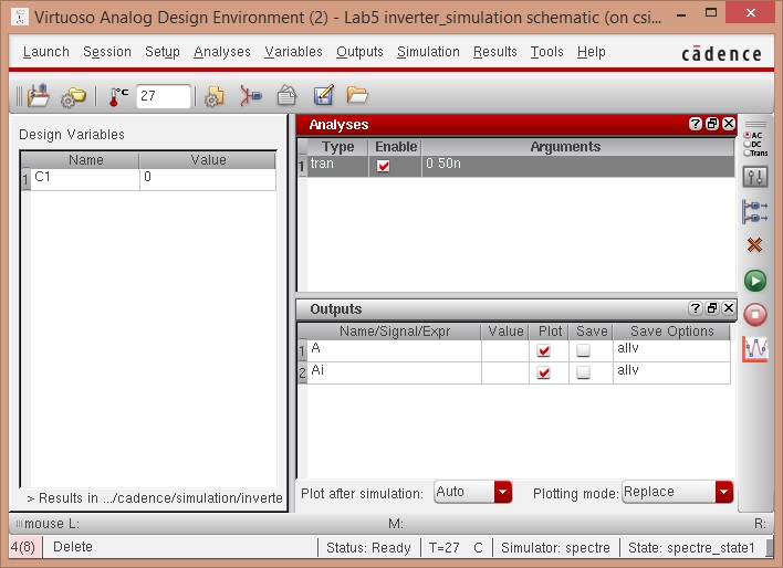
I chose to use a variable for the capacitor in order to display all of the values on the same plot. The simulation setup is seen below:
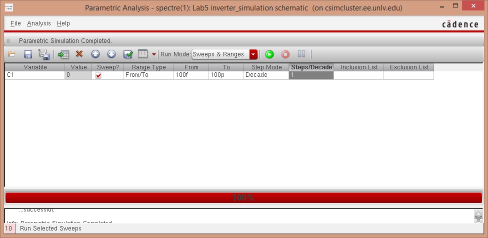
Next I do a parametric sweep of the C1 variable. The setup is seen below:
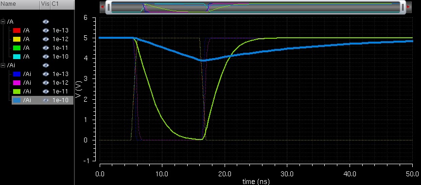
Finally it's time to run the simulation. All of the different results are seen below:
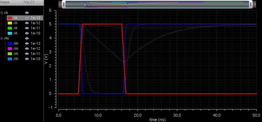
100f
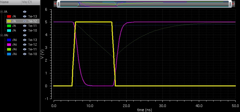
1p
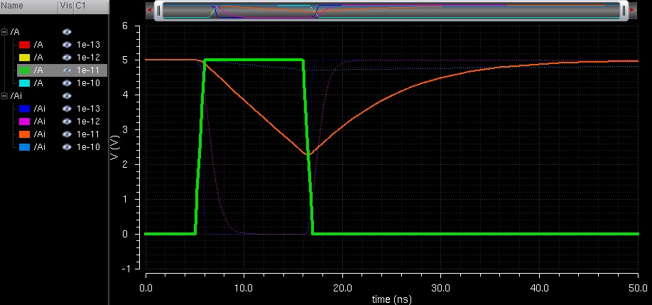
10p
100p
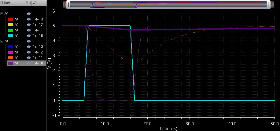
As the capacitance of the load increases, the poorer the inverter performs
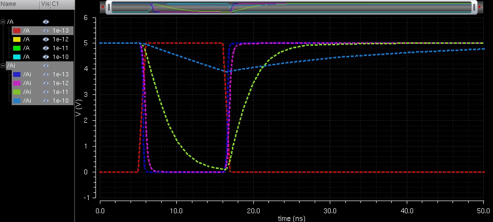
Next we will simulate the second inverter. The schematic is seen below:
Just like before, I set up the simulation and do a parametric sweep. The resulting simulation is found below. The bolded blue and green lines show the results for the 1p and 10p loads. They show significant improvement over the first inverter. The rest of the results are also in this image but it is hard to see. Check the zip file at the end of this page for more clear results.
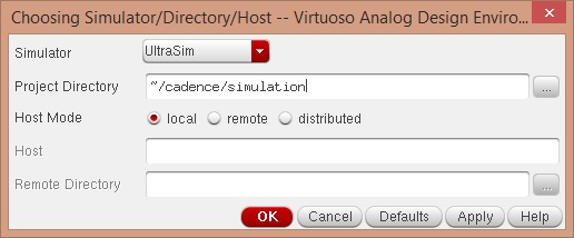
The final task of this lab is to repeat both simulations using Cadence's Ultra Sim. The setup is seen below:
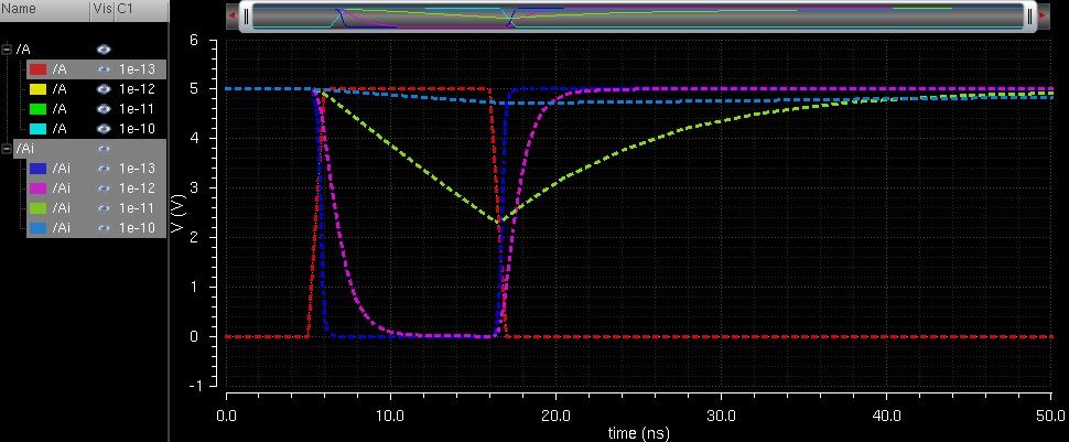
The results for the simulation of the first inverter is seen below:
The results for the simulation of the second inverter is seen below:
By using Ultra Sim, we seem to get very similar results than the initial simulations.
The lab is now complete. All of the work from this lab can be found in the zip file lab5.zip
Back