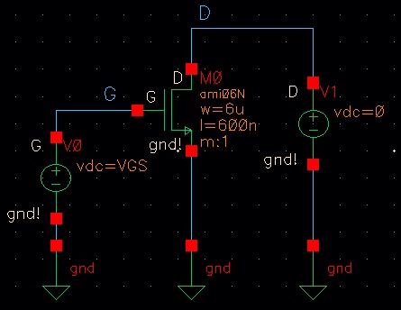
Below is the schematic for the circuit we will be simulating:
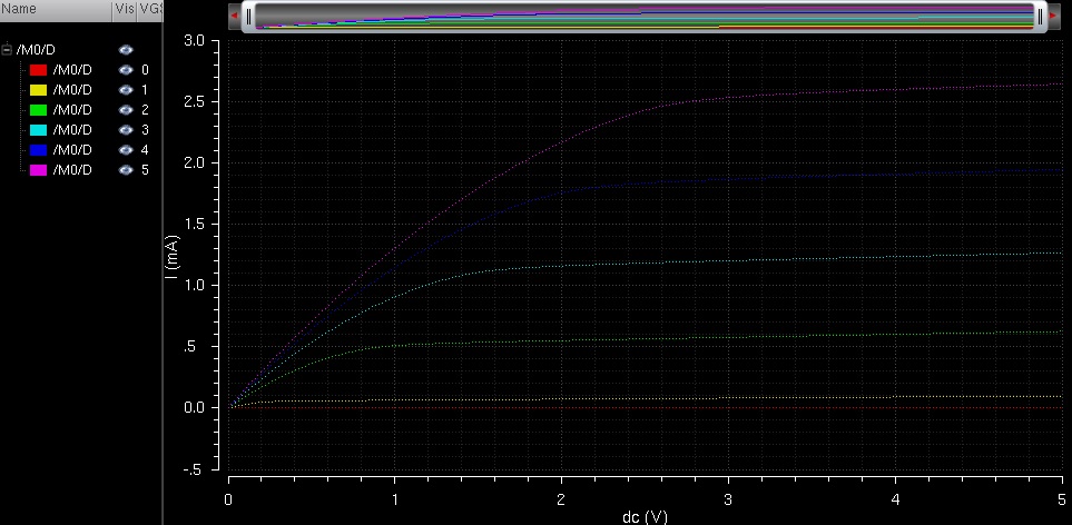
The simulation results can be found below:
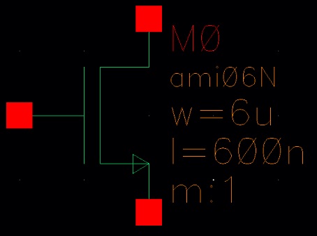
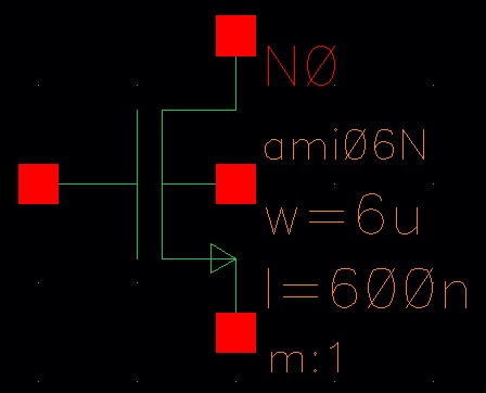
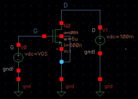
Next we will design the 4-terminal NMOS device:
The schematic can be seen below:
Next is the simulation of the 4-terminal PMOS device which can be found below:
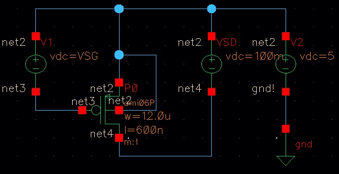
The schematic of this 4-terminal PMOS is the following:
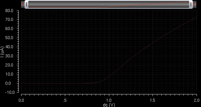
Finally the simulation of the 4-terminal PMOS device is found below:
The rest of this lab is incomplete.