Lab 4 - EE 421L
Authored
by Christopher Mikhael,
Email: Mikhaelc@unlv.nevada.edu
10/5/2014
The
Objective of this lab is to create both an NMOS and PMOS device with a
width of 6um which can be used for other projects. We also want to test
the NMOS and PMOS devices by graphing IV curvers for the MOSFETs.
First we started the lab by following tutorial 2.
NMOS Transistor
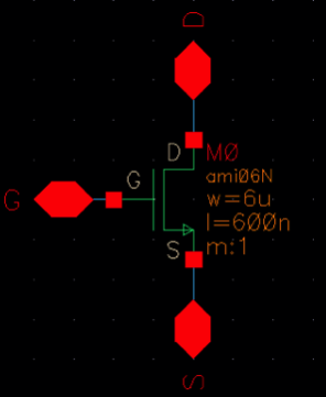
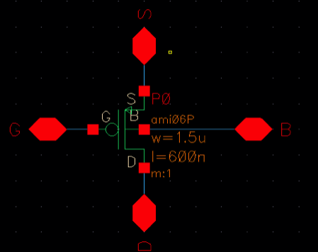
We first start by creating the NMOS transistor. To do this we used the transistor already found in the NSCSU_Analog_Parts library nmos4. This is a 4 terminal nmos resistor. We then added pins to all the inputs of the transistor as shown below:
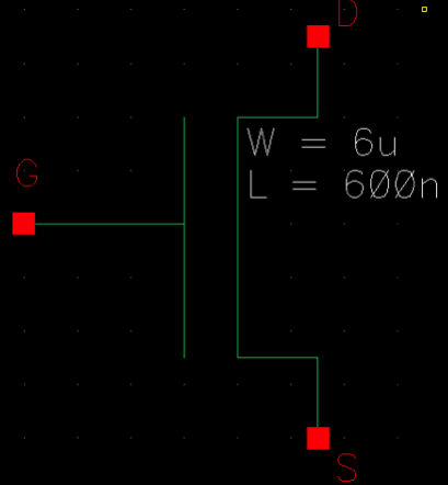
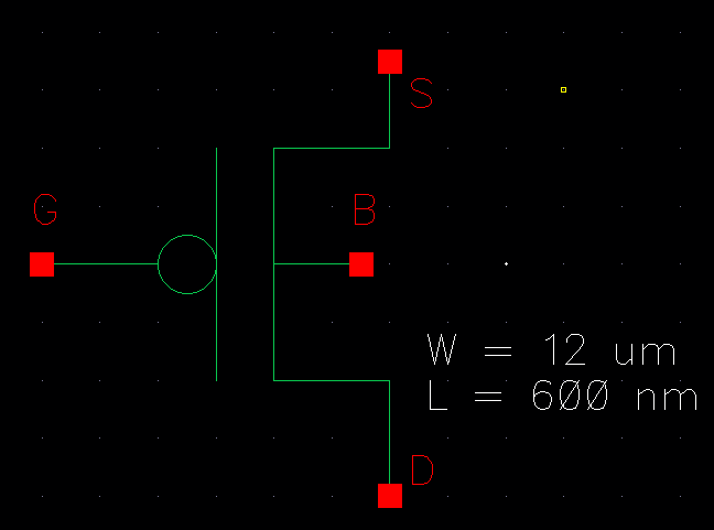
After saving the schematic, the next step is to design the symbol of
the component. This is not completely necessary but is sometimes
useful. Drawn symbol is shown below:
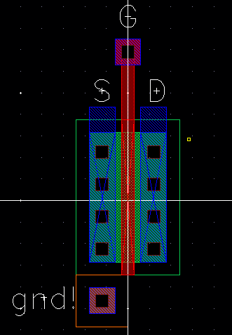
We now need to create the layout for this device. After opening the
layout window we place the same 4 terminal transistor used in schematic
4 and change the width of the device to 6um in the NSCSU_Analog_Parts
library.

We then placed a ptap next to the layout which will act as our ground
for the layout since NMOS devices uses a psubstrate. We also place
m1_poly to the layout which will be the metal1 connector for the gate. These asre found in the NSCSU_TechLib_ami06 library.
For the Source and Drain terminals a metal1 layer is extened and labeled with D or S as shown below:
We first perform a DRC check to make sure the device meets all design
rules then extract the layout. In the extracted view we then check if
the device can properly LVS.
PMOS Transister
The same steps are performed for the PMOS transistor except the Source
and Drain are set opposite. Also when creating a schematic using this
device the bulk must be set to vdd instead of gnd. We will be using the
width of 12um.
We start by creating the schematic and symbol as seen below using the pmos4 transistor in the NSCSU_Analog_Parts library:
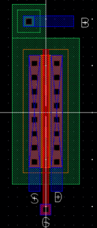
Next the layout was made using the same part as the schematic. Here we
have to make sure to change the width to 12um when placing the instance
down. We then can use an ntap to represent the bulk terminal which is
placed on vdd when used in a schematic. Also place the m1_poly to make
th connections to the gate. These componenets can be found in the
NSCSU_TechLib_ami06 library. Then place the apropriate metal
connections to the tranistor as shown below with the correct labels:
We then need to DRC the layout to make sure that the layout doesn't
violate any of the design rules. After this is complete we can extract
the layout and LVS making sure the layout matches the schematic.
NMOS Simulations
Now that we have our transistors complete we can
use them to view their IV characteristics. First we will look at the ID
v. VDS for an NMOS and also the ID v. VGS.
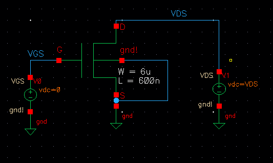
First we will have to create a schematic which can be used to view the
ID v. VDS characteristics. For this we want to sweep VGS from 0 to 5V
in 1V increments and view it when VDS is between 0 and 5 V in 1mV
steps. This will all be performed using the 6u/600n width-to-length
ratio.
The following schematic was created to view the simulation:
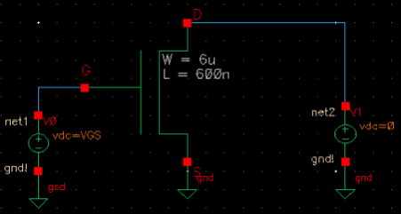
Note that V0 is set to VGS so that the parameter can be swept.
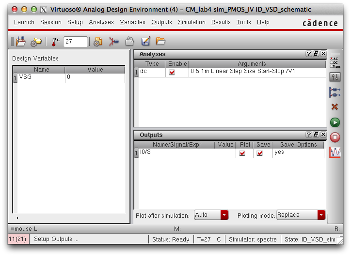
Next we have to configure the ADE window to perfom the schematic. To do
this we first have to make sure the ADE is in spectre. We then have to
import the ami_06 models so that they can be simulated. To do this we
go to setup>>model libraries. Then add a new model which in this
case will be in: /$HOME /ncsu-cdk-1.6.0.beta/models/spectre/standalone.
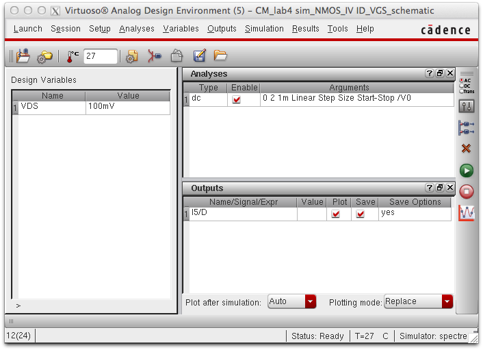
The analyses have to be set next, this is done with the following configuration:
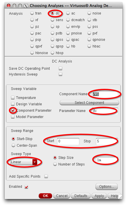
The points that we want to plot from the schematic have to also be set. In this case the Drain.
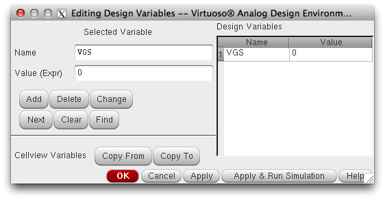
We then want to sweep VGS from 0 to 5V this is done by going to variables edit and creating a variable for VGS at 0V:
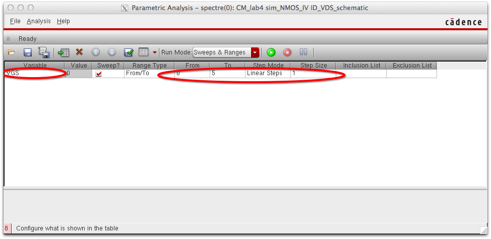
Next go to tools>> parametric analyses and set VGS from 0 to 5
volts. This is where we will run the simulation from. The simulation
will not work properly if ran in the main ADE window.
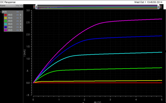
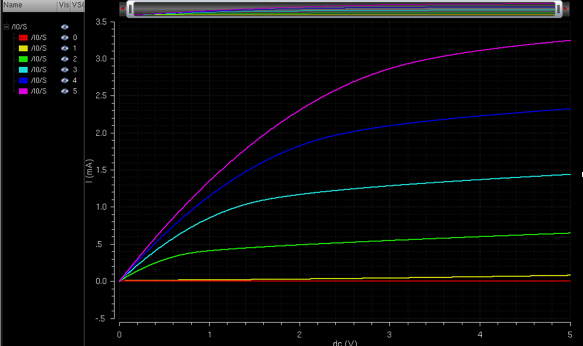
After we run the simulation we should see the ID vs VDS graph for different VGS inputs as shown below:
ID v VDS
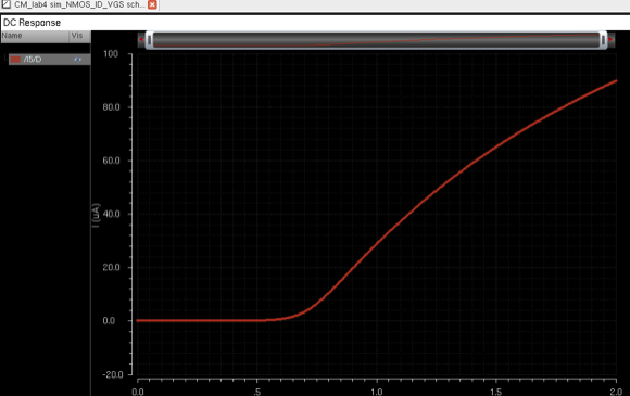
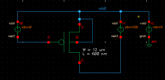
For the ID v VGS we have to change the schematic so that VGS is set to zero and we set VDS to parameter VDS as shwon below:
The only difference with the ADE is that we add the VDS variable with a
value of 100mV. 100mV can also be set in the schematic and does not
have to be a parameter. There will be no parameter sweep for this
graph. We also need to set VGS to vvary from 0 to 2 V in 1 mV
increments. This is done in the analyses window.The graph is shown
below:
ID v. VGS
PMOS Simulations
For the PMOS the steps are similar but the schematic and variables are configured differently.
Here we make VSG the parameter that will be sweeped. We also have to
make sure that the bulk is connected to vdd instead of gnd. We will
also be reading from the source for PMOS instead of the drain.
When simulating we obtain the following(be sure to add the model for the pmos):
ID v. VSD
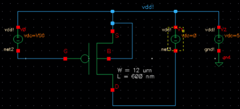
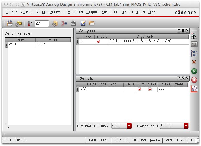
When creating the ID v. VSG for the PMOS we use the following schematic.
Notice the VGS is set to 0 and V1 is set to VSD. We must also change
the parameters in the ADE so that VSD has a value of 100mV and the
analysis runs from 0 to 2V in 1 mV steps.
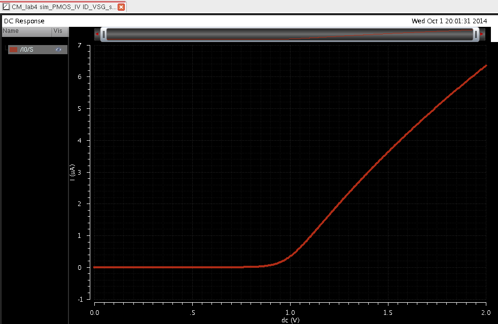
ID v. VSG
Probe Pads
To add probe pads we first must add the lab 4 library into our CMOSedu directory. This will provide the probepads that will be used for this portion of the lab.
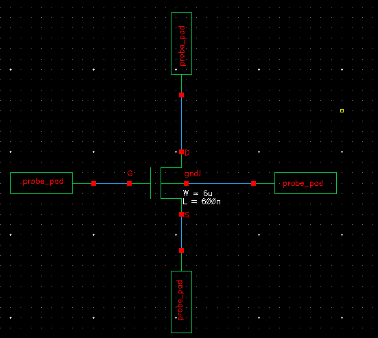
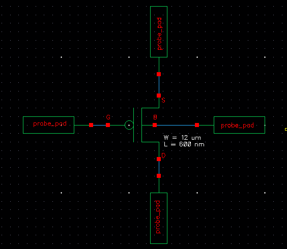
We then need to create a new schematic and add the NMOS/PMOS transistor
we made earlier. We then connect all the outputs to the probepads found
in lab 4. The schematic should look like this:
NMOS
|
PMOS
|
 |
|
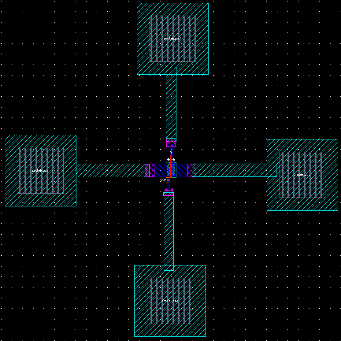
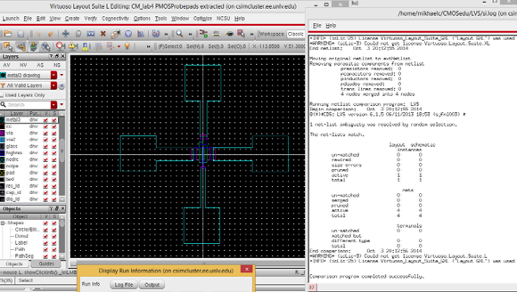
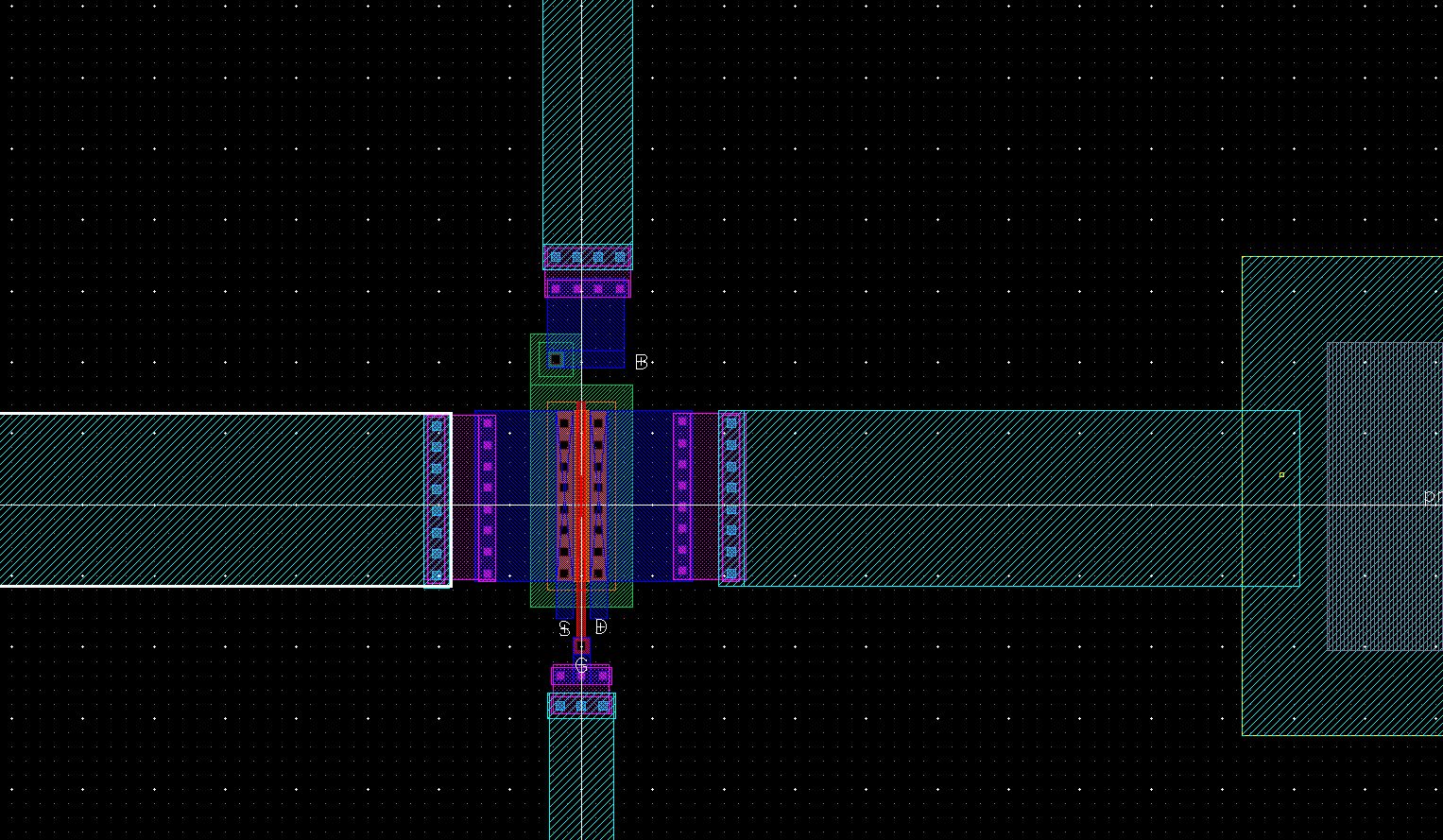
After this is saved and checked we will create the layout. To
do this we have to place the instance of the NMOS transistor and the
probpads. When placing the probepads be sure to provide adequate space.
It is good practice to DRC any big changes made to make sure there is
no violation of the design rules.
The next part will be to transition from a metal 1 connection to a
metal 3 connection. Since these metals indicate different layers on the
chip we have to connect them in order. To go from metal 1 to metal 2 we
will use the m2_m1 connector from the NCSU_TechLib_ami06. We can then
extend metal 2 and add a m3_m2 connector. After this is performed it is
important to DRC to make sure the PADs are still spaed correctly. Then
make the final metal 3 connection to the pads this is shown below:
Connections(metal1>> m2_m1>> metal2>>m3_m2>> metal3):
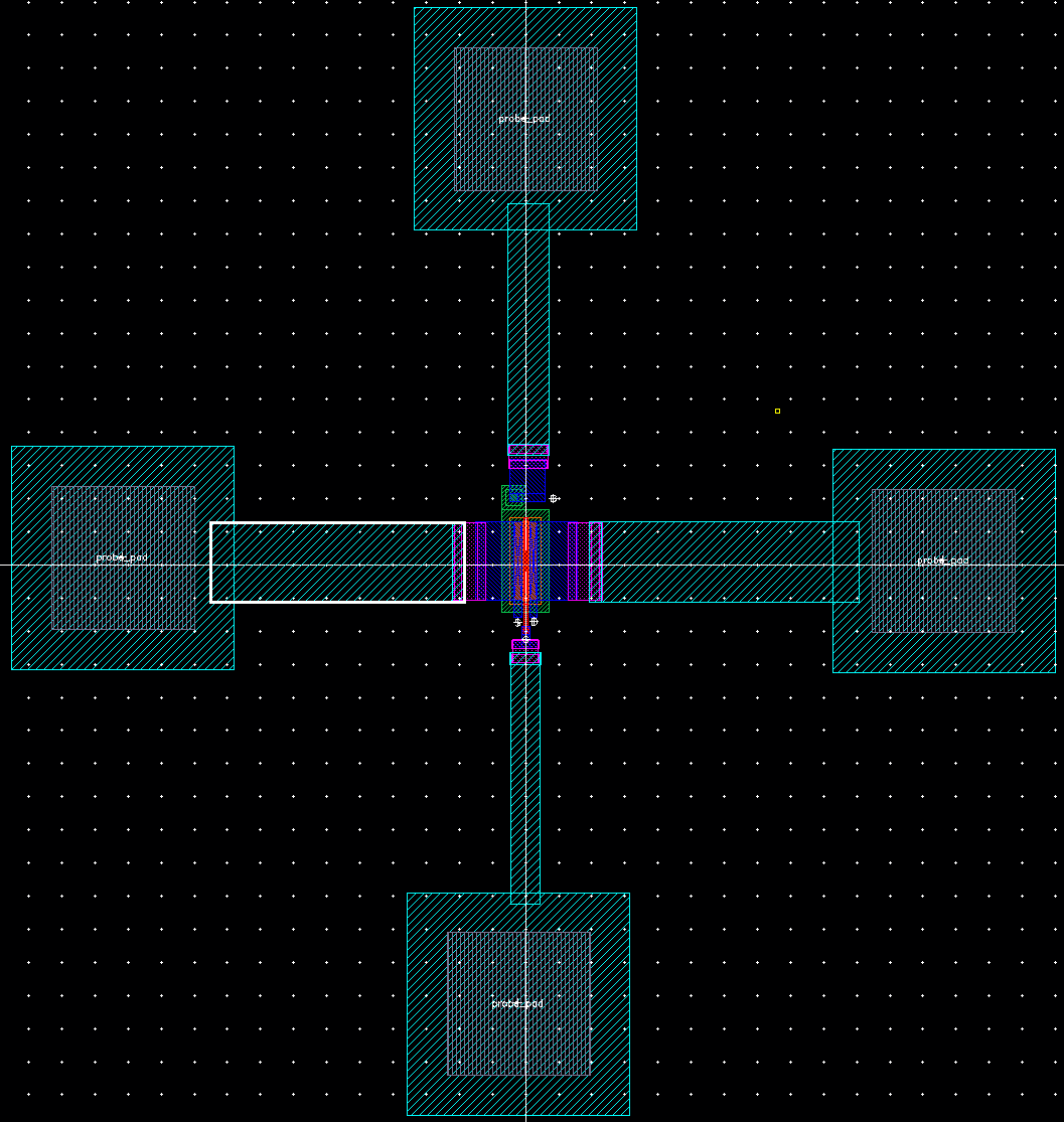
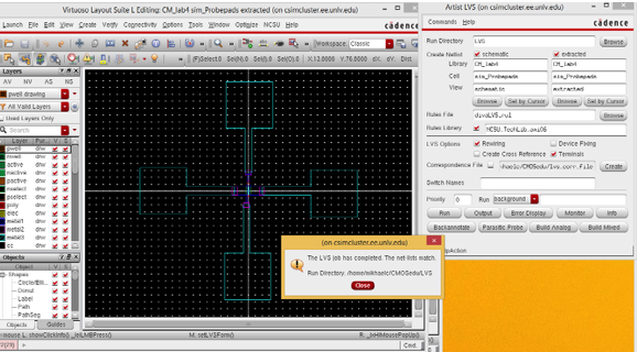
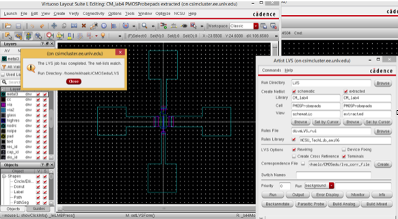
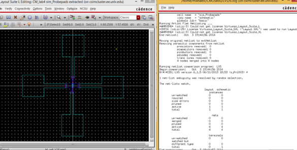
After making the connections we have to extract the file and then LVS
the extracted file with the schematic. If all is done correctly there
should be no errors as shown below:
This concludes the lab. To view the actual layout files click here: CM_lab4.zip