Lab Project - EE 421L
Authored
by Abel De La Torre,
delatorr@unlv.nevada.edu
11/10/2014
Project
-To design, layout, and simulate an 8-bit ALU that can perform: A AND B,
A OR B, A + B (addition), and A - B (subtraction).
First
half of the project (no layout just schematics and symbols), of
your design and an html report detailing operation (including
simulations).
Create an 8-bit ALU that can perform the following four operations:
A AND B
A OR B
A + B (addition)
A - B (subtraction)
Project stars by creating a new library called "EE_421L_AD_f14_Project".
The components created in lab 7(EE_421_lab7_AD_f14) are used in the project.
There are 5 components needed to make an ALU: OR gates, AND gates, inverters,
2to1 MUXes, and a full adder. This is the list of components:
2-input AND gate
2-input NAND gate
2-input OR gate
2-input NOR gate
2-input NOT gate
2-input MUX gate
This library includes the 8-bit version of each component listed above as well as an 8-bit Full Adder.
Up to this point all previews work used in every lab can be reference to the tutorials listed on the class web page
seen here.Part I: ALU Schematic and symbols
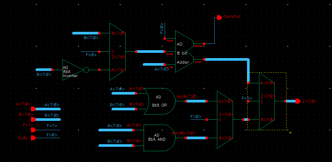
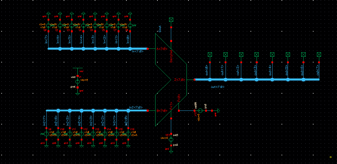
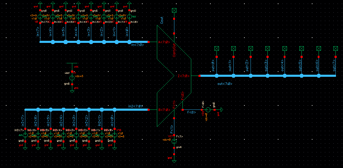
This
is what the 8 Bit ALU schematic looks like. As shown , From top
to bottom, the schematic consists of and AND gate an 8 bit inverter
connected to an 8 bit 2-1 Mux. The AND gate and
the 8 bit 2-1 Mux are connected to and 8 Bit Carry ADDER. At the
bottom of the chematic there's an 8 Bit AND gate and an 8 Bit OR gate
each with 2 inputs connected to an 8 Bit 2-1 Mux.
The Top arrangement is the MATH section of the ALU and the bottom
arrangement is the LOGIC section of the ALU. Both MATH and LOGIC
arrangements are connected to 8 Bit 2-1 Mux to the far right of the schematic.
The following shows the top ALU schematic checked and saved and showing no errors.
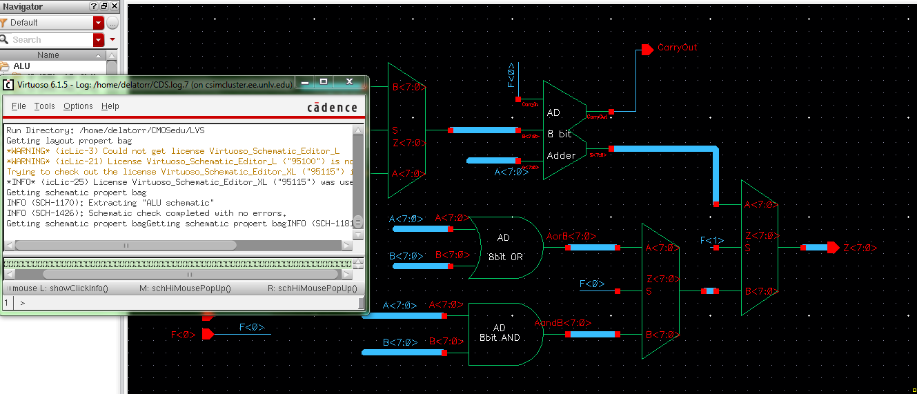
This is a closer look of the Comand Interpreter window showing no errors for the ALU schematic.

For
the schematic shown above, The following displays the
corresponding ALU Symbol created after the schematic it has a total 6 pins
for input
and output.

After
the representation of the ALU Schematic and its parts as well as the
symbol created, I move un to the simulation of the ALU using Test
schematics to test for the requirements of the lab (A and B, A or B, A + B, A - B).
MATH Section of ALU:
ADD Test Schematic
First I start with the MATH section of the ALU, The ADD and SUB parts of it.
This is the Test Schematic for the ADD test part of this lab ( A + B)
The control signal: F0= 0V
F1 = 5V
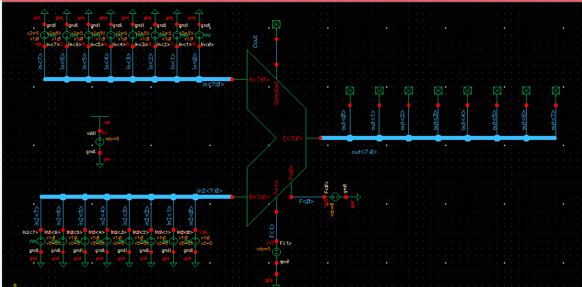
The
following represents the inputs or INPUTS 1 and INPUTS 2 that are
ADDED. For our test procedure we will select the following inputs
which are marked on the simulation:
INPUT 1: 0 1 1 0 0 0 0 1
INPUT 2: 0 1 0 1 0 1 1 1
The following is the representation of the inputs for the above calculation.
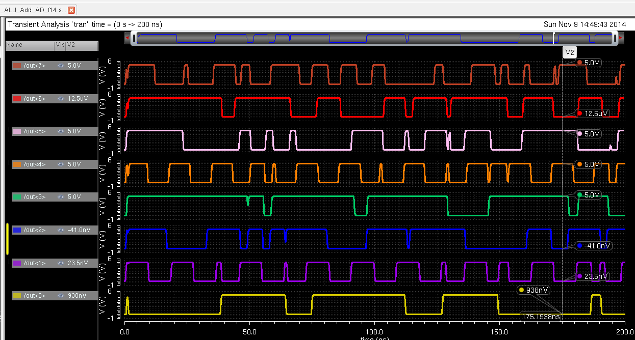
Simulation marker displays: 5V = 1 ( High )
0V = 0 ( Low
) note: Simulation shows values for (Low) to be
insignificantly close to zero

As expected the previews ADD calculations shows the correct output shown below.
INPUT 1: 0 1 1 0 0 0 0 1
INPUT 2: 0 1 0 1 0 1 1 1
OUTPUT:
1 0 1 1 1 0 0 0
SUBTRACTION Test Schematic
Now
we test the Subtraction section of the ALU. The following
displays the test schematic for the SUBTRACTION feature and this is the
bynary numbers to be subtracted.
To perform this calculation, 2's
complement is performed. Recalling the ALU schematic above, The
CIN part of the AND gate on the top part of the schematic along with
the 8 bit inverter represents the 1 Bit that is to be added to complete
the calculation.. The following is the bynary calculation to be
performed:
This is the corresponding test schematic for the SUBTRACTION section of the ALU.
The control signal: F0= 5V
F1 = 5V
INPUT 1: 1 0 1 1 0 1 0 1
INPUT2: 0 0 1 1 1 1 1 0
The following is the representation of the inputs for the above calculation.
Simulation marker displays: 5V = 1 ( High )
0V = 0 ( Low ) note:
Simulation shows
values for (Low) to be insignificantly close to zero
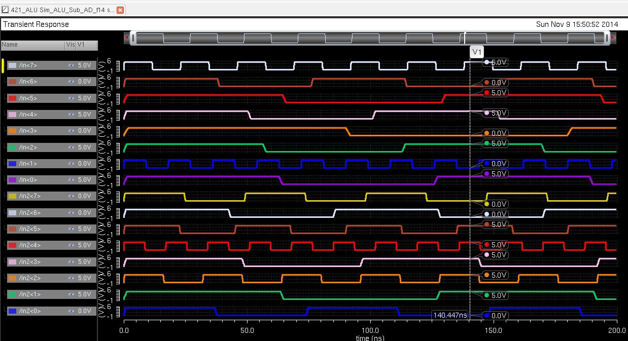
This is the complete SUBTRACTION calculation with the coresponding answer.
INPUT 1: 1 0 1 1 0 1 0 1
INPUT2: 0 0 1 1 1 1 1 0
OUTPUT 0 1 1 1 0 1 1 1
The following simulation shows the correct output for the the top subtraction calculation.

LOGIC Section of ALU:
AND Test Schematic
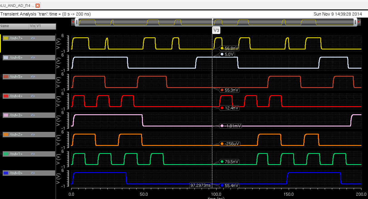
Now we move on to the bottom section of the ALU schematic shown at the very top, the LOGIC nsection of the ALU.
we begin with AND calculation. The follwoing represents the test schematic of the AND calculation of the ALU.
The control signal: F0= 0V
F1 =0V
INPUT 1: 1 1 0 0 0
0 1 0
INPUT 2: 0 1 1 0 1 1 0 1
The following is the representation of the inputs for the above calculation.
Simulation marker displays: 5V = 1 ( High )
0V = 0 ( Low ) note:
Simulation shows
values for (Low) to be insignificantly close to zero
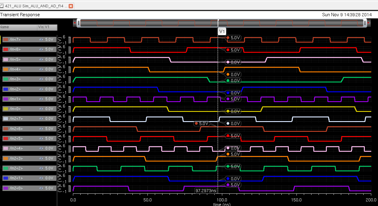
This is the complete AND calculation with the coresponding answer.
INPUT 1: 1 1 0 0 0 0 1 0
INPUT 2: 0 1 1 0 1 1 0 1
OUTPUT: 0 1 0 0 0 0 0 0
The following simulation shows the correct output for the the top subtraction calculation.
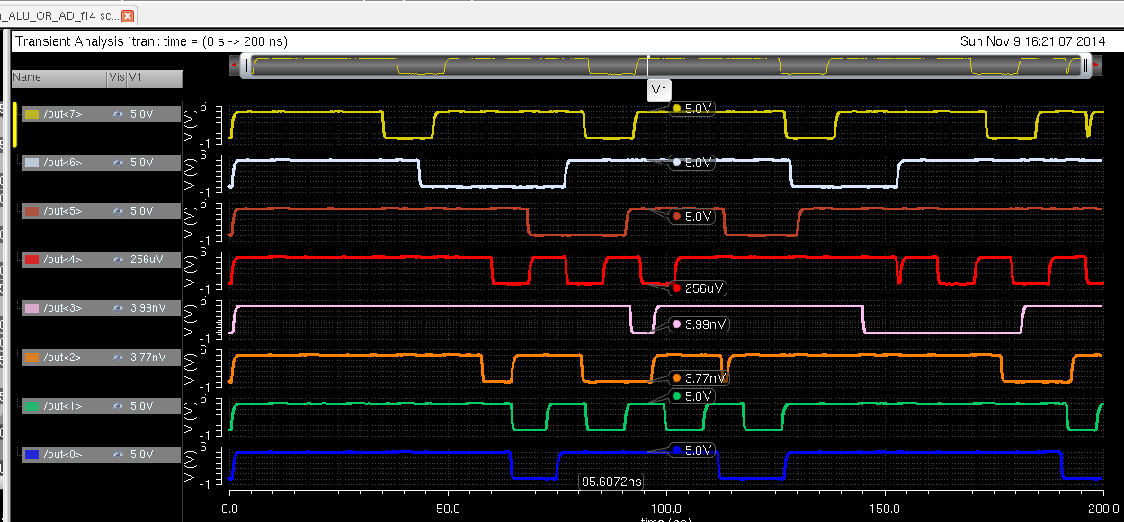
ORTest Schematic
Finally, the OR calculation. The following represents the test schematic for the OR test schematic.
The control signal: F0= 5V
F1 = 0V

INPUT 1: 1 1 0 0 0 0 1 0
INPUT 2: 0 1 1 0 0 0 0 1
The following is the representation of the inputs for the above calculation.
Simulation marker displays: 5V = 1 ( High )
0V = 0 ( Low ) note:
Simulation shows
values for (Low) to be insignificantly close to zero
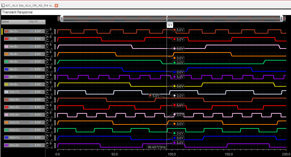
This is the complete OR calculation with the coresponding answer.
INPUT 1: 1 1 0 0 0 0 1 0
INPUT 2: 0 1 1 0 0 0 0 1
OUTPUT: 1 1 1 0 0 0 1 1
The following simulation shows the correct output for the the top subtraction calculation.
Part II: The ALU Layout
8 bit AND gate:
Part
II of the project is create an 8bit ALU layout of the schematic
introduced in Part I. The following 8 bit layout is achieved by using
some of the 8 bit components previewsly created in lab 7
and 8 bit layouts created specifically for this project. The
aproach of creating 8 1Bit ALU's will not be used for this part of the
project.
I will start with the logic section of the ALU which includes an 8 bit AND gate, an 8 bit OR gate both connected to an 8 bit 2-1 Mux.
This is how the 1 bit AND gate layout looks like.

The following is the layout of the 8 bit AND gate.

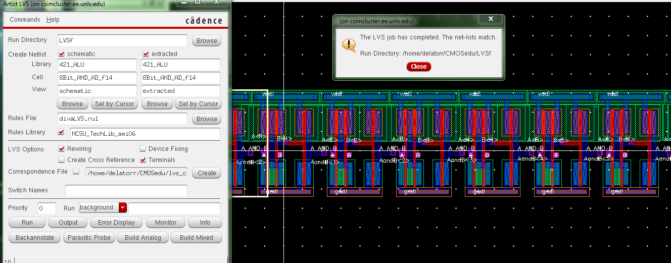
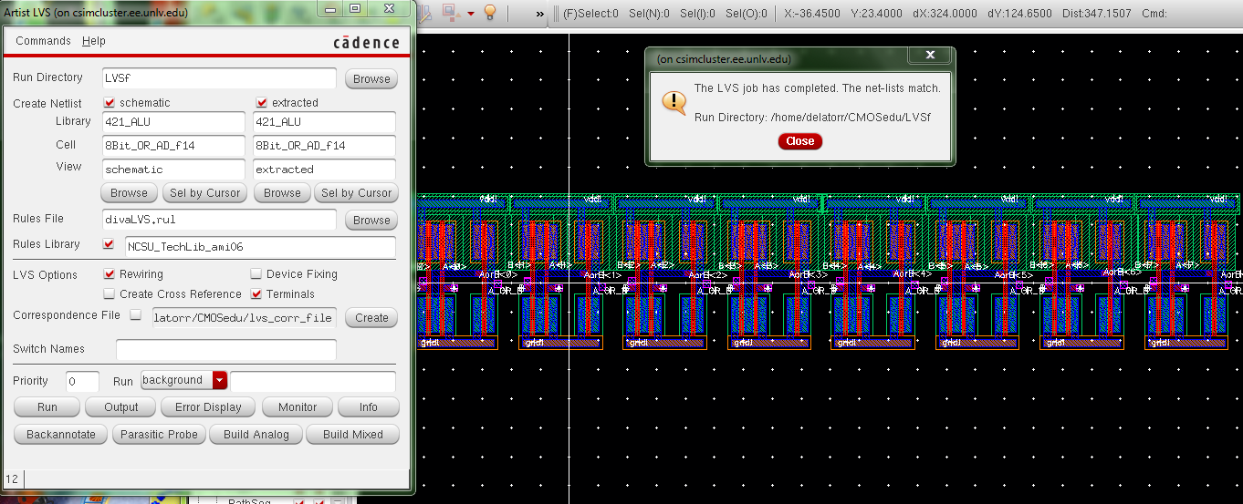
After DRC with no errors, the layout is extracted and LVS check shows a net-list match.
8 bit OR gate:
Continuing with the layouts, we move on to the OR gate. The following is the 1 bit layout of the Or gate.
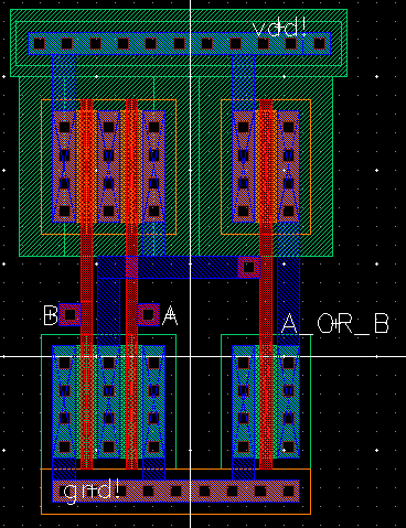
This the coresponding layout of the 8 Bit OR gate.
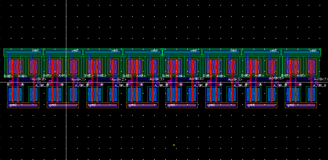
After DRC with no errors, the layout is extracted and LVS check shows a net-list match.
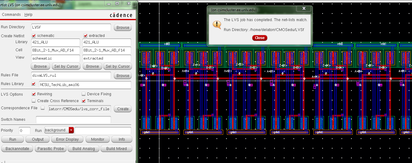
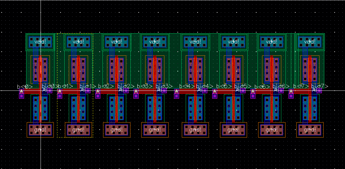
8 bit 2-1 MUX
In the logic section of the ALU the 8 bit AND and the 8 bit OR gates are connected to an 8 bit 2-1 MUX. The output of the 8 bit AND gate comes in through input B of the 8 bit MUX and the 8 Bit OR gate output comes in through the input A of the 8 bit 2-1 MUX.
This is the layout for the 1 bit 2-1 Mux

The following is the coresponding layout of the 8 bit 2-1 MUX.
After DRC with no errors, the layout is extracted and LVS check shows a net-list match.
8 bit Inverter:
Now we move to the math section of the 8 Bit ALU. From the Schematic we see an 8 bit Inverter with the output connected through input A of another 8 bit 2-1 MUX.
This is th elayout for the 1 bit Inverter.

The following shows coresponding the layout for the 8 bit inverter.
After DRC with no errors, the layout is extracted and LVS check shows a net-list match.

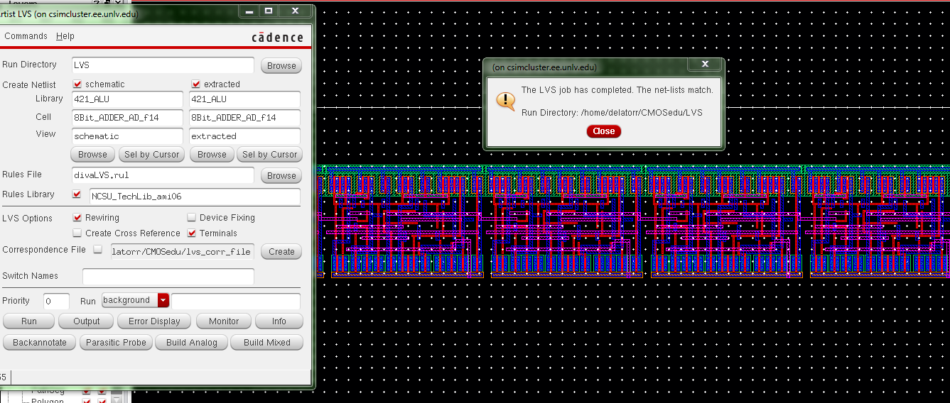
8 bit Full Adder:
Now
we move on to the 8 bit FULL ADDER created in Lab 7. As mentioned
the 8 bit INVERTER connects to the 8 bit 2-1 MUX and the 8 bit 2-1 MUX
connects to the 8 Bit Full ADDER in the math section of the 8 bit ALU.
The following shows the coresponding 8 bit FULL ADDER layout.

After DRC with no errors, the 8 bit layout is extracted and LVS check shows a net-list match.
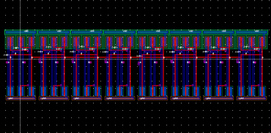
8 bit ALU:
Now that we have introduced the laouts needed, we move on to the layout of the 8 Bit ALU.
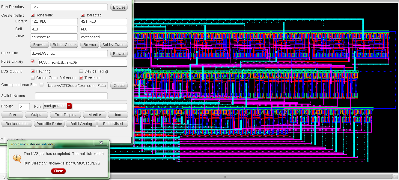
Acomplete laout of the 8 bit ALU.

Another look at the 8 bit ALU showing all its major componets.
The following displays the LOGIC section of the ALU as well as the MATH section of the ALU.
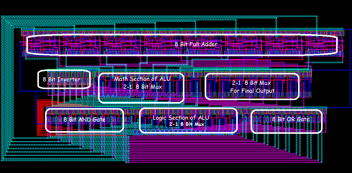
After DRC with no errors, the 8 bit ALU layout is extracted and LVS check shows a net-list match.
Zip up the file and get it ready to mail.

Email the file to yourself to secure its data.
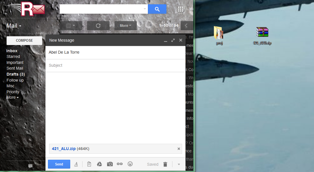
This concludes the 421 ALU project. The design directory coresponding to this project is found 421_ALU
Return to EE 421L Labs