Lab 08 - ECE 421L
Authored
by Jeevake Attapattu and Henry Chan
attapatt@unlv.nevada.edu, chanh6@unlv.nevada.edu
1 December 2014
Generating a test chip layout for submission to MOSIS for fabrication
For this lab we formed into groups to put test structures on a chip.
Each test circuit has its own power but ground is shared between the circuits.
Power is not shared between the circuits so that a vdd! to gnd! short in one circuit does not make other circuits inoperable.
Using MobaXTerm log into csimcluster.ee.unlv.edu. The first action is creating a backup. Type tar -cvf "date"CMOSedu.tar CMOSedu/. This will create a tar file
with all the project and homework saved. In place of "date" type in the
date creating the backup. Unce the backup has been created type gzip "date"CMOSedu.tar.tar. This will create a .tar.gz file witch is significantly smaller.
Use MobaXTerm to download the file to your own pc then upload to a backup site such as dropbox or google drive.

Launch Virtuoso.
You will be using previous work from tutorial 5 & 6.
Download all tutorials if needed from here.
In the library manager copy the files in lab 7 to lab 8.
Make sure that you update intances when copying.
Open
a new layout called pad since we are going to create a pad.
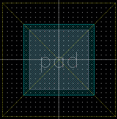
Start with the pad layer. The pad layer is going to be used later for
alignment purposes. According to the tutorial we need to use a
120umx120um pad.
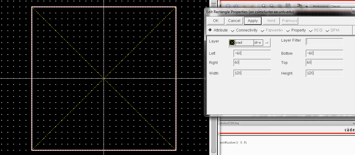
Use a 75umx75um metal 3 layer and
an overglass layer of 63umx63um. Notice that 75-63=12. That is 6um on
each side which is specified by the MOSIS design rules.
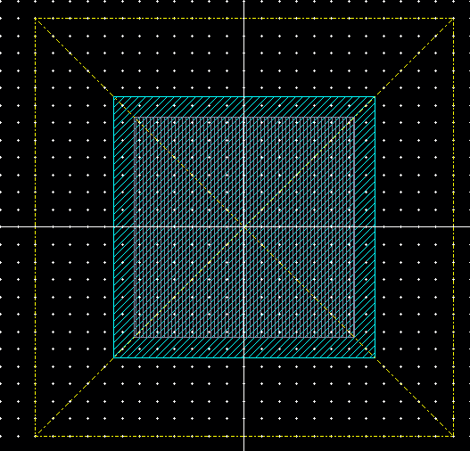
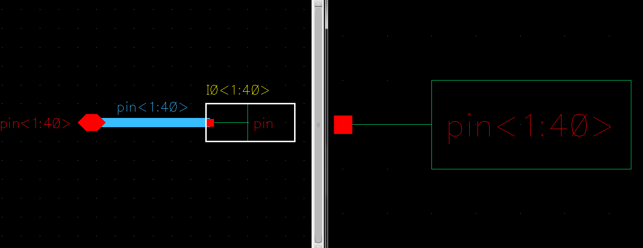
The last component is to add a pin on metal 3. Make sure that it is inputoutput and name it pad. Select the text and change the height. I chose 16.
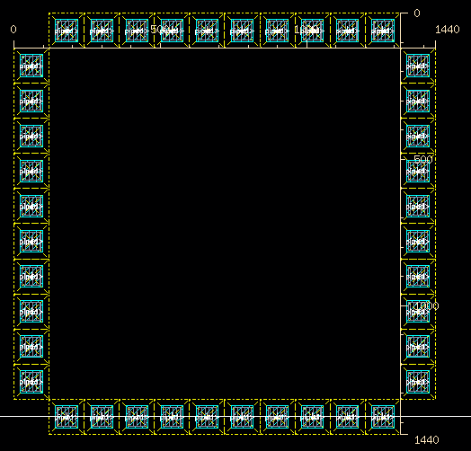
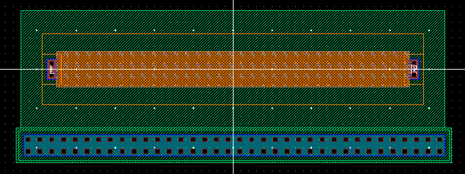
Next create a new layout called pad frame. Type i and place an instance of the pad you just created. Place another metal 3 inputoutput pin on top. Call it pin<1>. This notation is to indicate an array. Use c
to copy and select 12 rows and 12 columns. Delete the cells in the
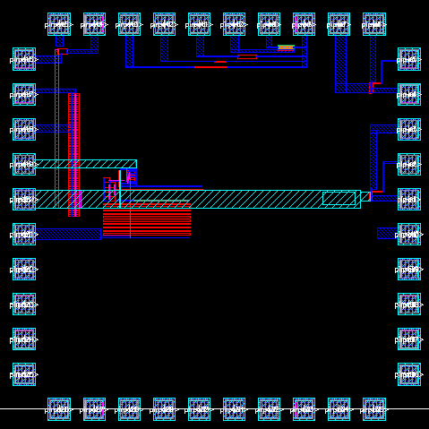
center and corners. You should have something similar to the
image below.
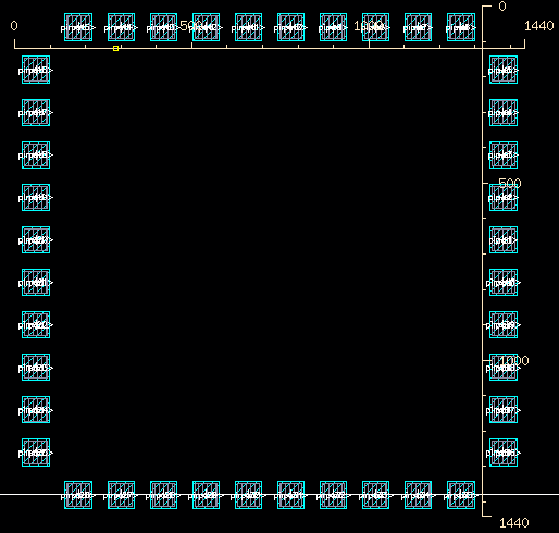
Now we need to number each pin individualy. Remove the pad layer on the pad layout.
This will help speed up selection. Follow the numbering scheme in the
tutorial. You should have something similar to the layout below.
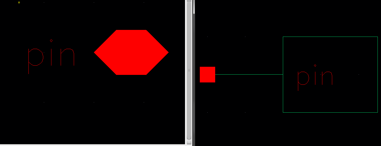
Now create symbol and schematic for the pad. For the schematic simply place an inputoutput pin called pad. Create the symbol and simplyfy as below.
Now do the same for the pad frame. As always DRC and LVS.
I later added metal1, metal2, via, and via2 so that my pads can connect with any metal layer.
The
rest of the tutorial involves adding additional items and connecting
them to the frame. We are going to skip that part becuase we will not be using that information in lab 8.
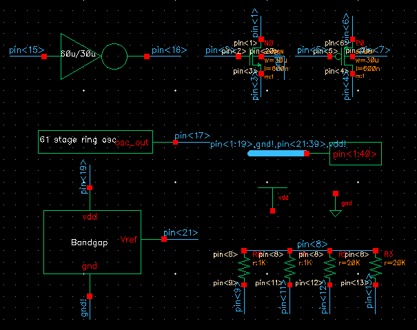
Our chip includes the following test structures:
- 30u/0.6u NMOS (3 pins,
DN, GN, SN, connect the p+ body, B, of the NMOS to the chip's ground
pin)
- 30u/0.6u PMOS (4 pins,
DP, GP, SP, and BP)
- Inverter made using 30u/0.6u NMOS and 60u/0.6u PMOS (3 pins, in, out, VDD_inv)
- 61 stage ring
oscillator using 6u/0.6u MOSFETs with off-chip buffer (2 pins, VDD_osc and Ocs_out. Ground connected to pin
20)
- 20k n-well resistor (2
pins)
- 20k hi-res poly
resistor (2 pins)
- 1k n+ resistor (2 pins)
- 1k p+ resistor (3
pins, need n-well to isolate the p+ from the p-substrate and the n-well
needs to be tied to a voltage >= either side of the resistor)
- Bandgap reference (2 pins, VDD_bg and Vref)
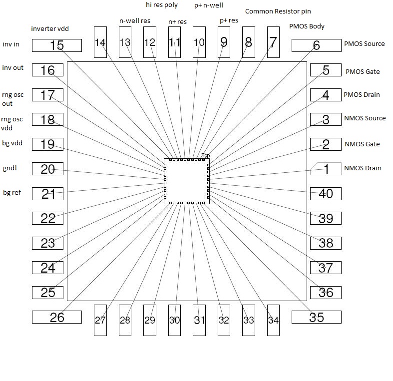
Our test tructures follow the following pin configuration:
| Test Structure | # of Pins | Terminal | Pin # | Notes: |
| NMOS 30u/0.6u | 3 | DN | 1 | Body connected to pin 20 (Ground) |
| GN | 2 | |
| SN | 3 | |
| PMOS 30u/0.6u | 4 | DP | 4 | |
| GP | 5 | |
| SP | 6 | |
| BP | 7 | |
| Inverter (30u/0.6u NMOS, 60u/0.6u PMOS) | 3 | VDD_Inv | 14 | Ground connected to pin 20 |
| In | 15 | |
| Out | 16 | |
| 61 Stage Ring Oscillator (6u/0.6u MOSFETs) | 2 | VDD_ocs | 18 | Ground connected to pin 20 |
| osc_out | 17 | |
| 20k N-Well Resistor | 2 | | 8 | |
| 13 | |
| 20k Hi-Res Poly Resistor | 2 | | 8 | |
| 12 | |
| 1k N+ Resistor | 2 | | 8 | |
| 11 | |
| 1k P+ Resistor | 3 | | 8 | |
| 9 | |
| N-Well | 10 | N-Well should be tied to VDD |
| Bandgap Reference | 2 | VDD | 19 | Ground connected to pin 20 |
| Vref | 21 | |
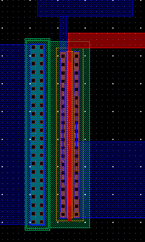
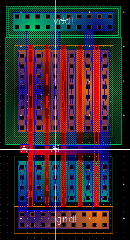
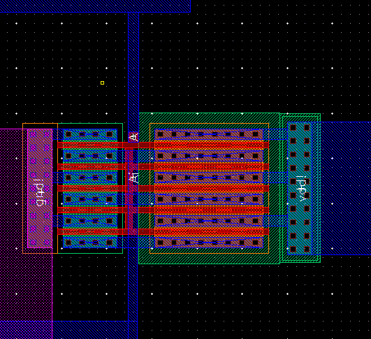
The Layout
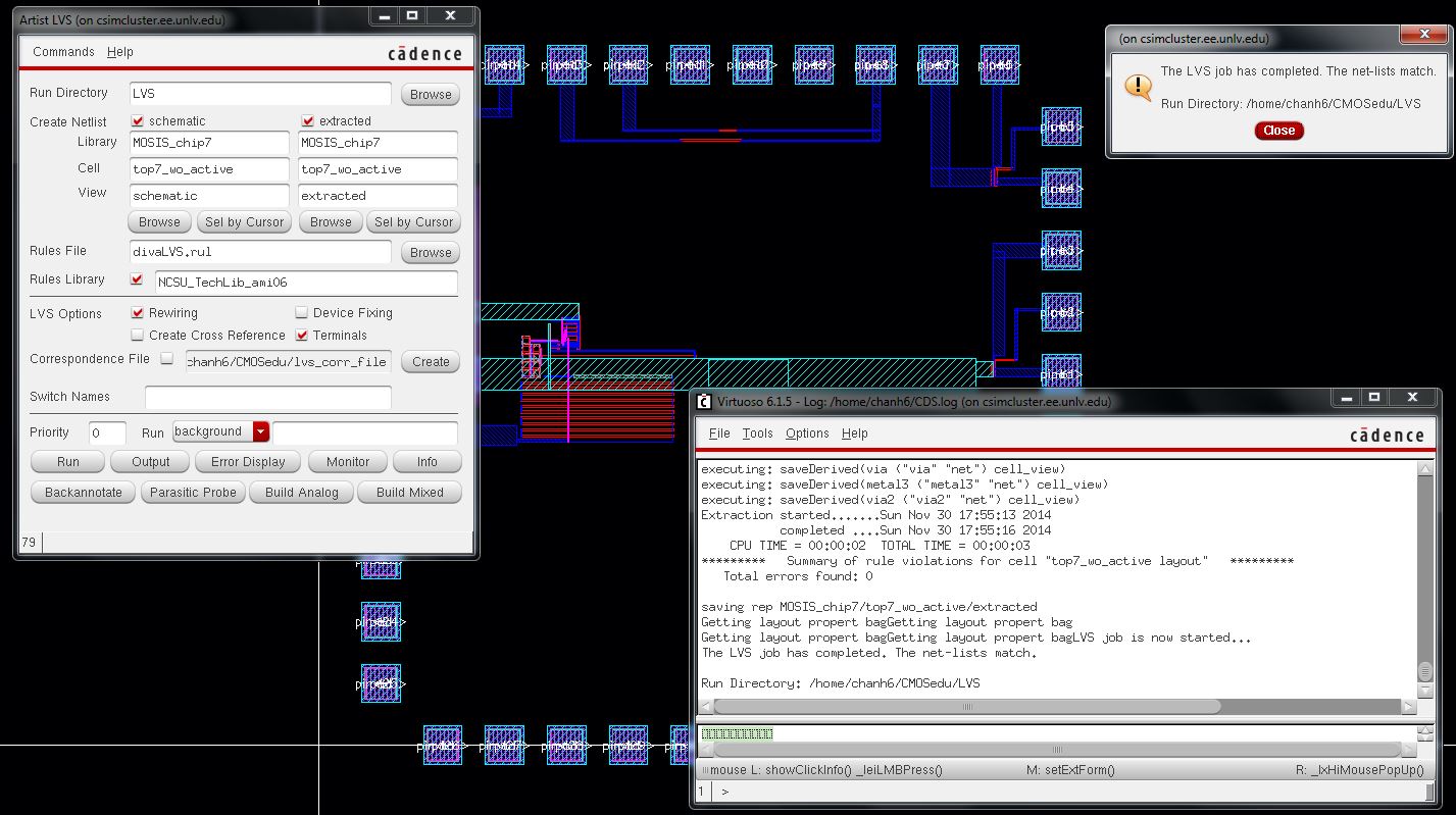
It DRCs and LVSs!
Test Structures:
30u/0.6u NMOS (3 pins, DN, GN, SN, with the body, B, connected to the chip's ground pin)
- The Drain (DN) is connected to pin 1
- The Gate (GN) is connected to pin 2
- The Source (SN) is connected to pin 3
The
NMOS is tested by applying 5V to the drain (DN), connecting the source
(SN) to gnd (ideally pin 20), and adjusting the voltage at the gate
(GN) to test the current through the NMOS. As you increase the gate
voltage above the threshold voltage, you should start to see the
current increase.
30u/0.6u PMOS (4 pins,
DP, GP, SP, and BP)
- The Drain (DP) is connected to pin 4
- The Gate (GP) is connected to pin 5
- The Source (SP) is connected to pin 6
- The Body (BP) is connected to pin 7
The
PMOS is tested by applying 5V to the source (SN), connecting the drain
(DN) to gnd (ideally pin 20), connecting the body (BP) to 5V, and
adjusting the voltage at the
gate (GN) to test the current through the PMOS. With 5V at the gate,
you should see 0 current. As you decrease the voltage to 5-Vthp
and below, the current will begin to increase.
Inverter made using 30u/0.6u NMOS and 60u/0.6u PMOS (3 pins, in, out, VDD_inv)
- VDD_Inv is connected to pin 14
- In is connected to pin 15
- Out is connected to pin 16
- GND is connected to pin 20 (gnd!)
The
inverter is tested by connecting VDD_Inv to 5V and gnd to 0V at pin 20
(gnd!). Applying 5V to In will result in 0V at Out and applying 0V to
In will result in 5V at out.
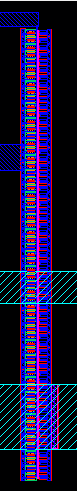
61 stage ring
oscillator using 6u/0.6u MOSFETs with off-chip buffer (2 pins, VDD_osc and Ocs_out. Ground connected to pin
20)
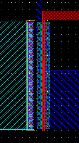
Click on the image for a closer view.

- VDD_osc is connected to pin 18
- osc_out is connected to pin 17
- GND is connected to pin 20 (gnd!)
This
ring oscillator operates at a frequency of ~87 MHz. To test, simply
connect VDD_osc (pin 18) to 5V and GND to pin 20 (gnd!). Ambient noise
should start the ring oscillator. By connecting osc_out to an
oscilloscope you can examine the waveform. The waveform should show a
square wave from 0V to 5V with a duty cycle of 50% and frequency of
87MHz.
Resistors:
All resistors share pin 8 as a terminal to demonstrate pin efficiency.
For all resistors, the test methods are very similar:
Apply a known voltage across the resistor's terminals at pin 8 and their other respective terminal pin.
Measure the current with an ammeter and use Ohm's Law (V=IR) to obtain the resistance.
A
special case exists for the 1k p+ resistor where you must connect pin
10 to a voltage greater than or equal to the voltage across the
resistor in order to prevent current leakage.
20k n-well resistor (2
pins)
The sheet resistance is approximately 800 Ohms. This requires 25 squares. We have used 111.6um x 4.5um.

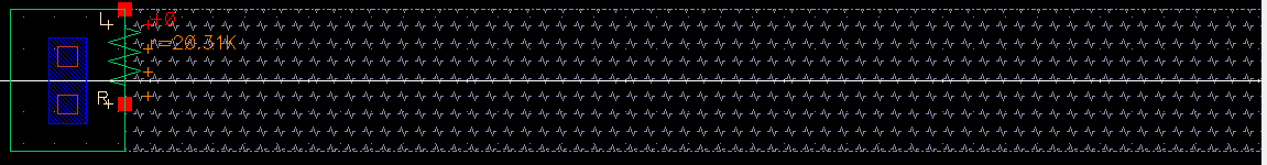
- One terminal is connected to pin 8
- The other terminal is connected to pin 13
20k hi-res poly
resistor (2 pins)
The sheet resistance is approximately 1k. This requires 20 squares. We have used 36um x 1.8um.
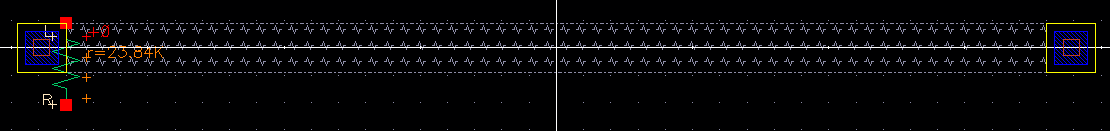
- One terminal is connected to pin 8
- The other terminal is connected to 12
1k n+ resistor (2 pins)
- One terminal is connected to pin 8
- The other terminal is connected to 11
1k p+ resistor (3
pins, need n-well to isolate the p+ from the p-substrate and the n-well
needs to be tied to a voltage >= either side of the resistor)
- One terminal is connected to pin 8
- The other terminal is connected to pin 9
- A third connection needs to be made to ensure the n-well does not source current from the resistor.
- This
third connection is tied to pin 10 and needs to be tied to a voltage
that is greater than the voltage at either side of the resistor during
testing.
Bandgap reference (2 pins, VDD_bg and Vref)
- VDD is connected to pin 19
- Vref (1.25V) is connected to pin 21
- GND is connected to pin 20 (gnd!)
The
bandgap reference is intended to provide a constant 1.25V across
varying tempatures and VDD values. Connect GND to pin 20 (gnd!) and
sweep VDD (pin 19) from 3V to 5V to observe the effects of Vref (pin
21). Simulations show a relatively stable 1.25V when VDD is between 3.7
to 5V and may show dips in the Vref when VDD is below 3.7.
Here is the design directory used for this lab.
___________________________________________________________________________________________
Return to EE 421L Labs