
Lab 6 - ECE 421L

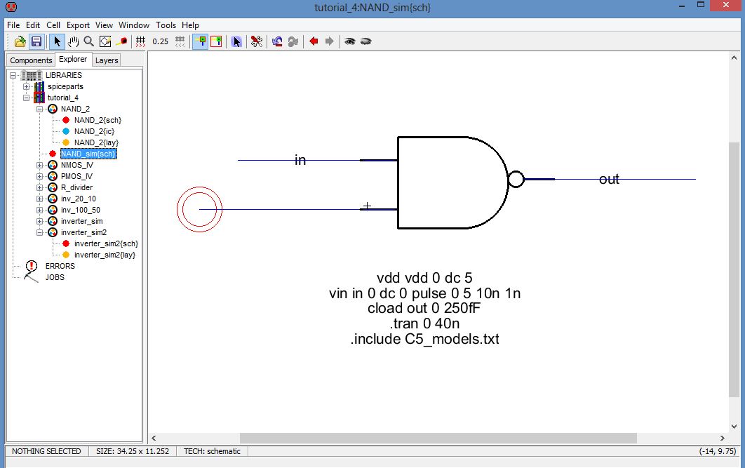
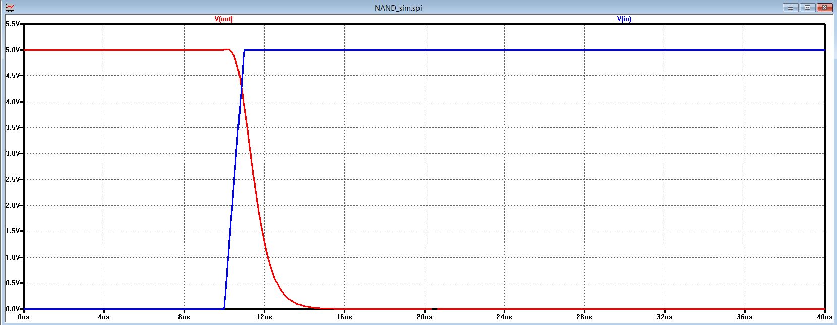
3. After checking the design, let's simulate the NAND gate. Connect one input to VDD and give a pusle signal to other input node. The following shows the sim_NAND and the simulation result.
4. Now move to lay out the NAND cell. The inv_20_10 contains the MOSFET layout. Only change the PMOS size and reconnect the nodes. Follow the steps shown in tutoral_4. The final layout is shown in following. Make sure the layout pass DRC, ERC and NCC.

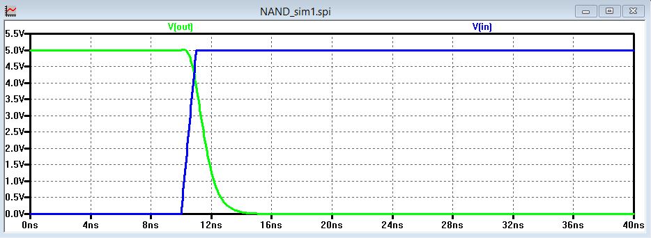
5. We also need to simulate the NAND layout. Connect B to VDD and give an input pusle to A node. See the AnandB simulation result.

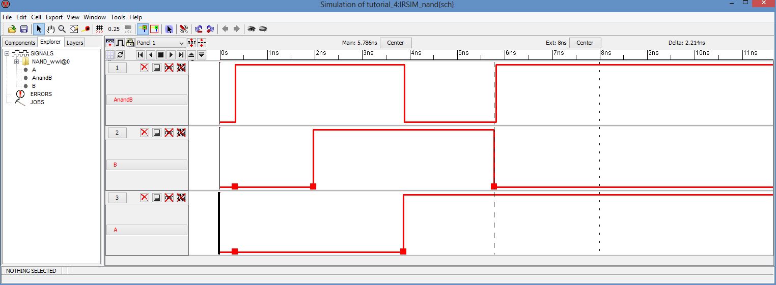
6. Use the LTpice and IRsim simulate the NAND gate. Open a new cell for simulation and insert the NAND icon. Then write down the spice code. This is for LTspice simulation. For IRSIM, another new cell should be opened and follow the steps discussed in the lab5 to run the IRSIM. The following images show the two simulation results and cells. As we know, for NAND gate, the output will be zero when both inputs are one. So the simulation is correct.


NOR gate design:
1. NAND gate can make the NOR gate much easier. Both gates use 4 MOSFETs and the change is the connection. And the size of PMOS is 20/2. Duplicate the NAND cell including the schematic, icon and layout cells. Then change the wire connection in the shematic. The right connection is shown in the following image.
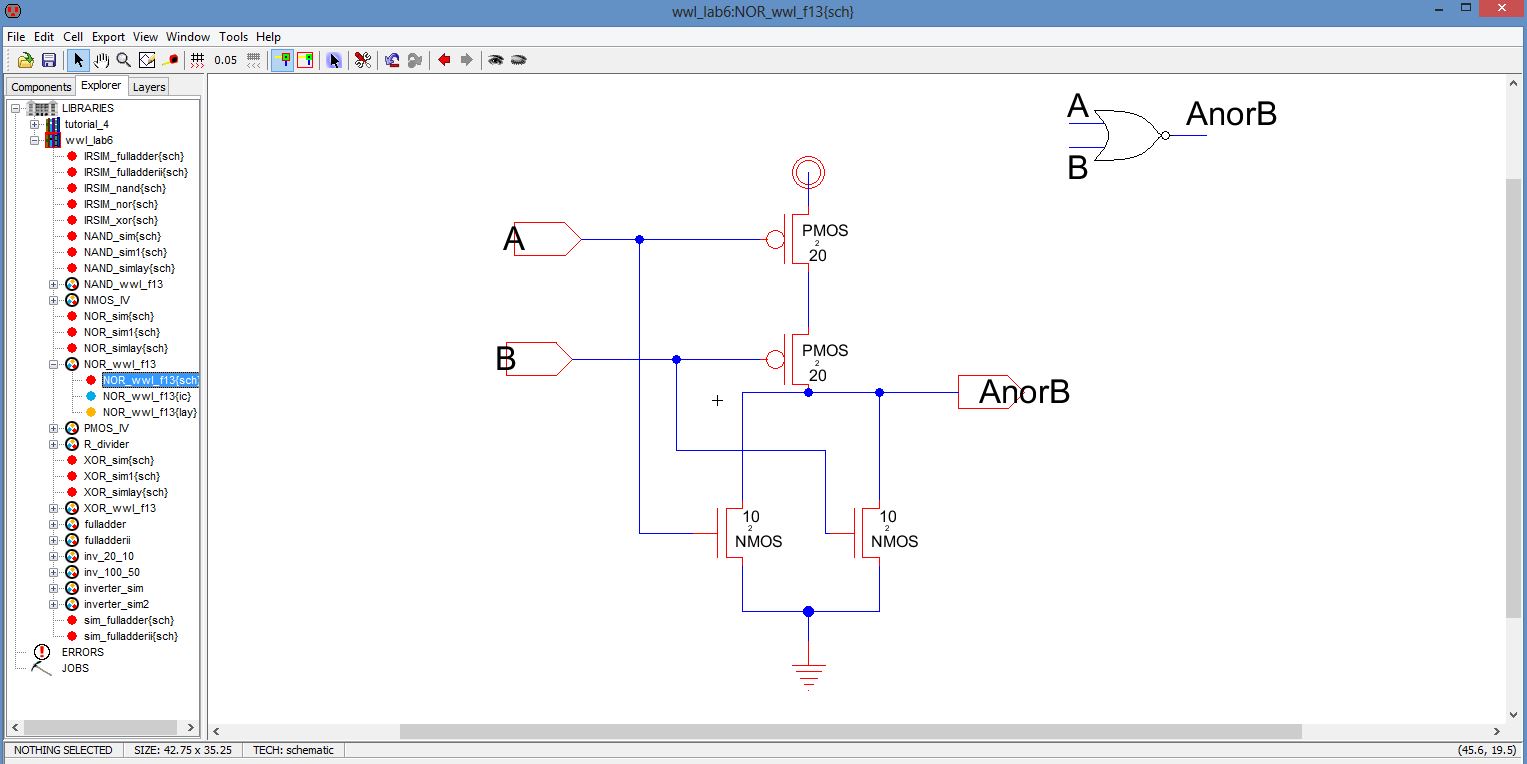
2. Next, the icon design is much difficult. Three splines need to be used and the icon is shown as seen below.

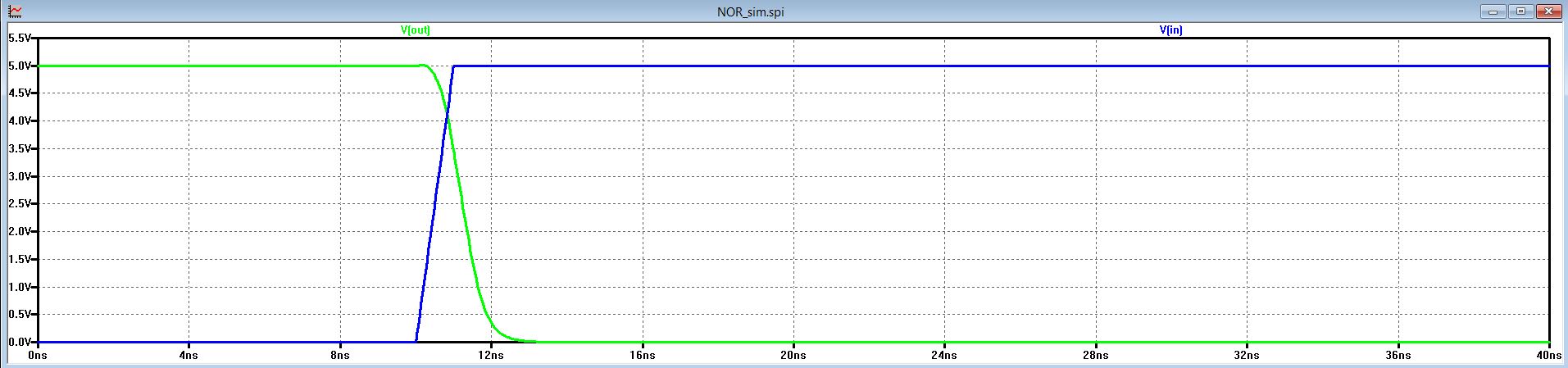
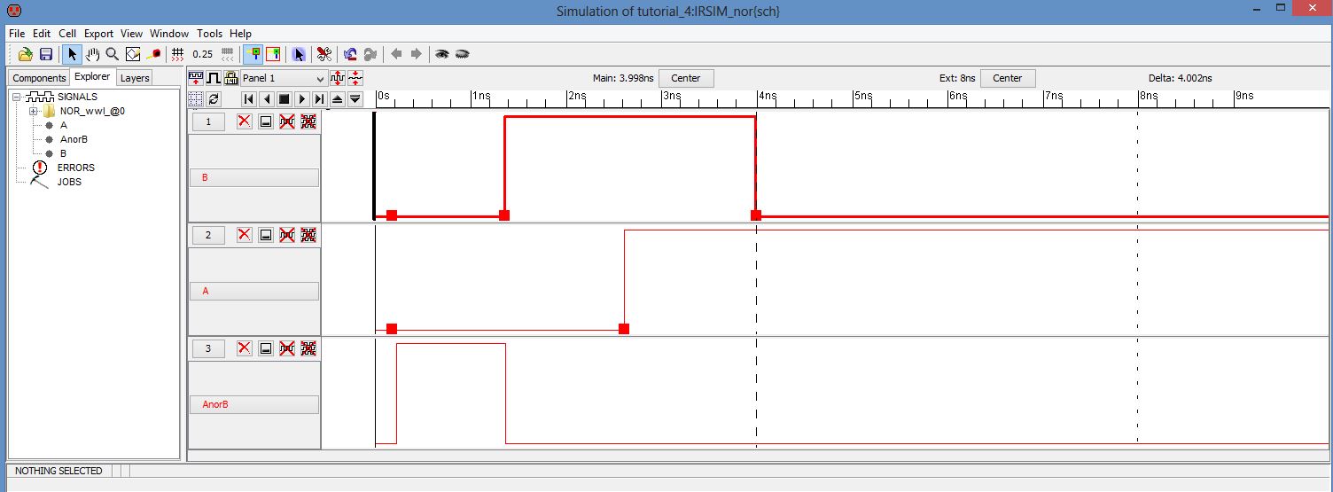
3. As the NAND cell design, simulate the NOR gate. Differently, connect B node to gnd and put a pulse signal to A node. Get the following simulation.

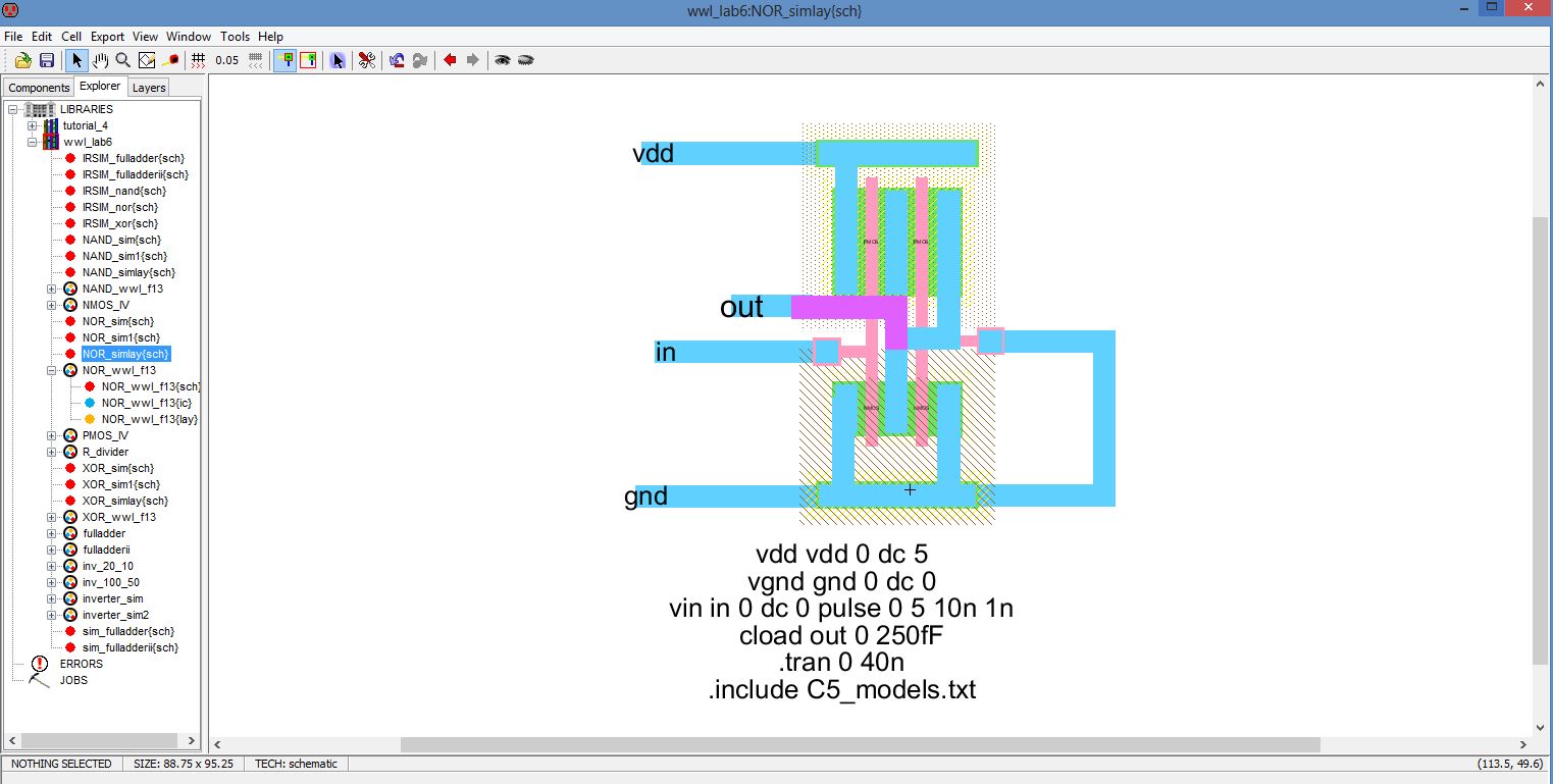
4. Then lay out the NOR gate. Based on the NAND layout, we only need to re-connect the MOSFETs. The following shows the right layout circuit and the simulation cell and result.


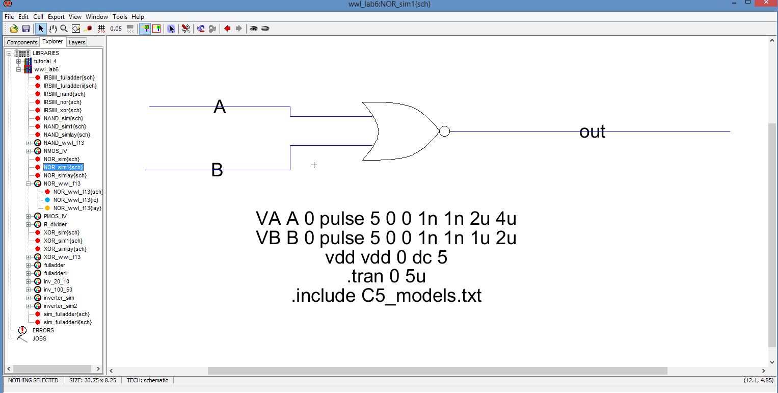
5. Next, it's to use LTpice and IRSIM for simulation. NOR gate will get the high output when inputs are both zero. The simulation proves it.

XOR gate design:
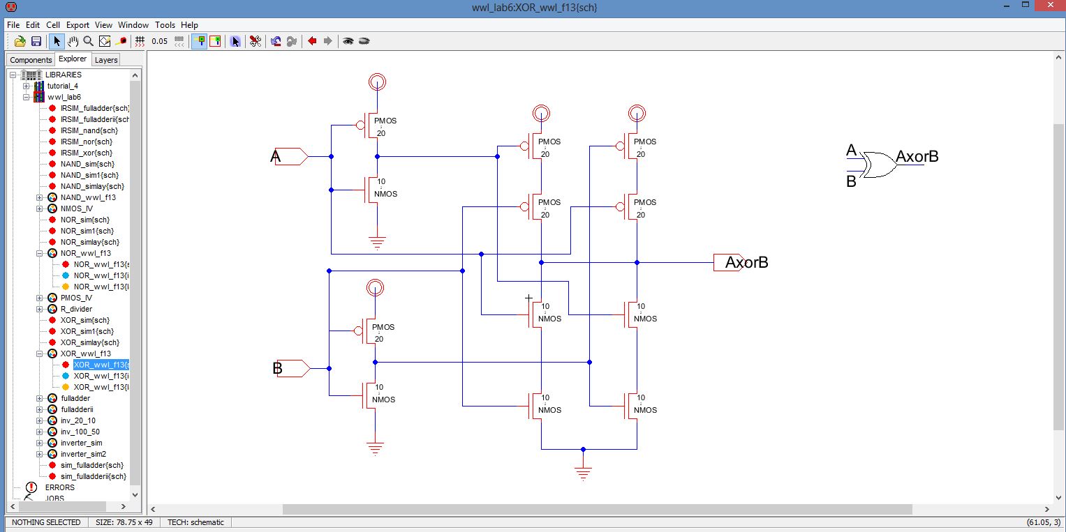
1. Fig. 12.18 shows the circuit topology of XOR gate. Two extra inverters are needed in this design. We can see 12 transistors will used in XOR gate. The size of PMOS is 20/10 and keep the size of NMOS unchanged. After designing NAND and NOR gates, the XOR is much easier. Duplicate the XOR gate again. And get 12 transistor in the new cell: XOR_wwl_f13. The correct circuit is shown in the following.
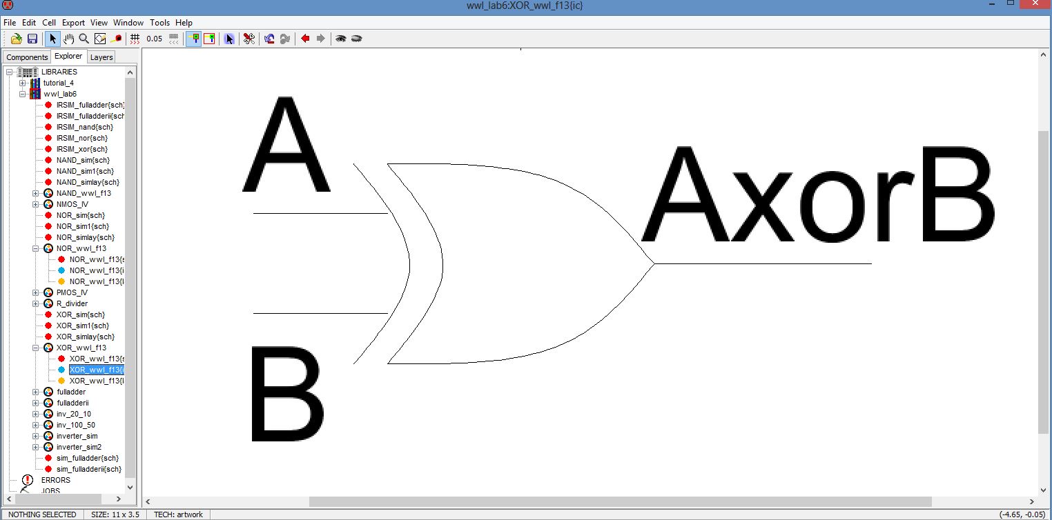
2. The icon view nearly looks like NOR gate. we need to change as seen below.
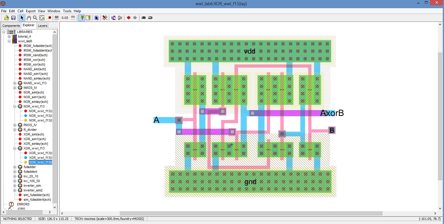
3. Before we move to the simulation, let's design the layout. Because it has 12 transistors, we need more time. Put every transistors in the standard cell frames that snap together end-to-end. Press F5 to check DRC.
4. Connect one input to gnd and give a pulse to other input node. We can see the following simulation result. I also do the same simulation at layout.

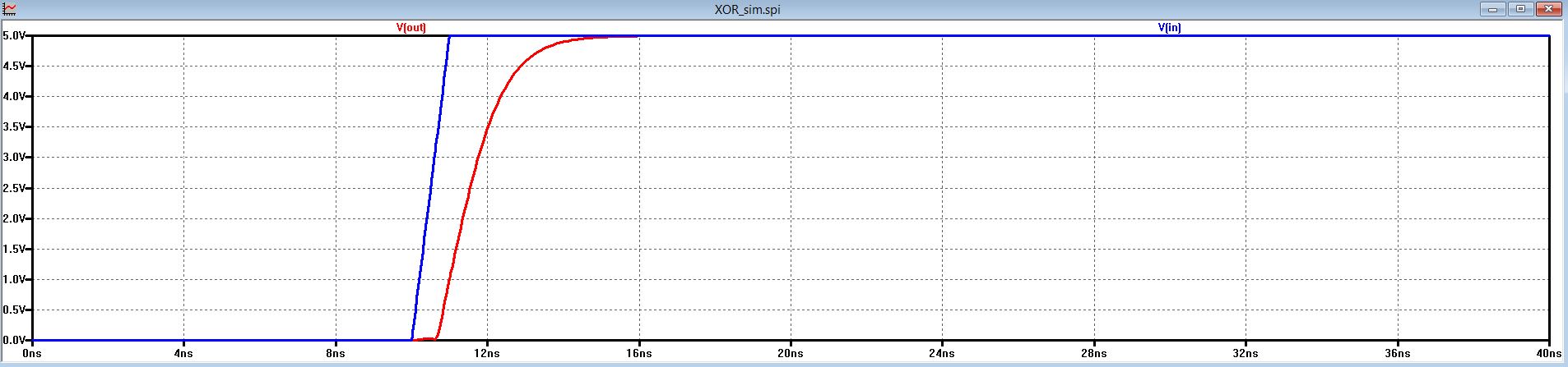


5. We also need to do the LTspice and IRSIM simulation. And the last figure is the IRSIM result. For XOR gate, the output will be high when two inputs are different. And the simulation proves it.


Full adder design:
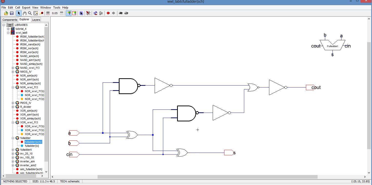
1. Now we have NAND, NOR, XOR gates. For the first full adder, use 2 XORs, 2 NANDs and 1 NOR with 3 inverters. Open a new cell: fulladder. And connect the wire Arcs as the figure shown in LAB6. Then make the icon depiced here.
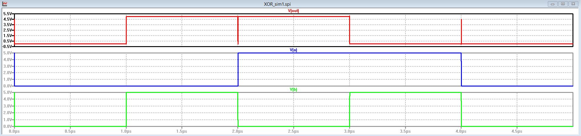
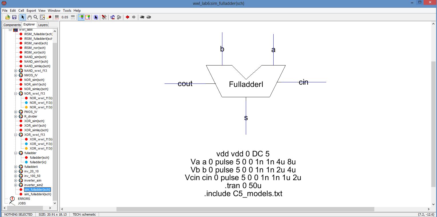
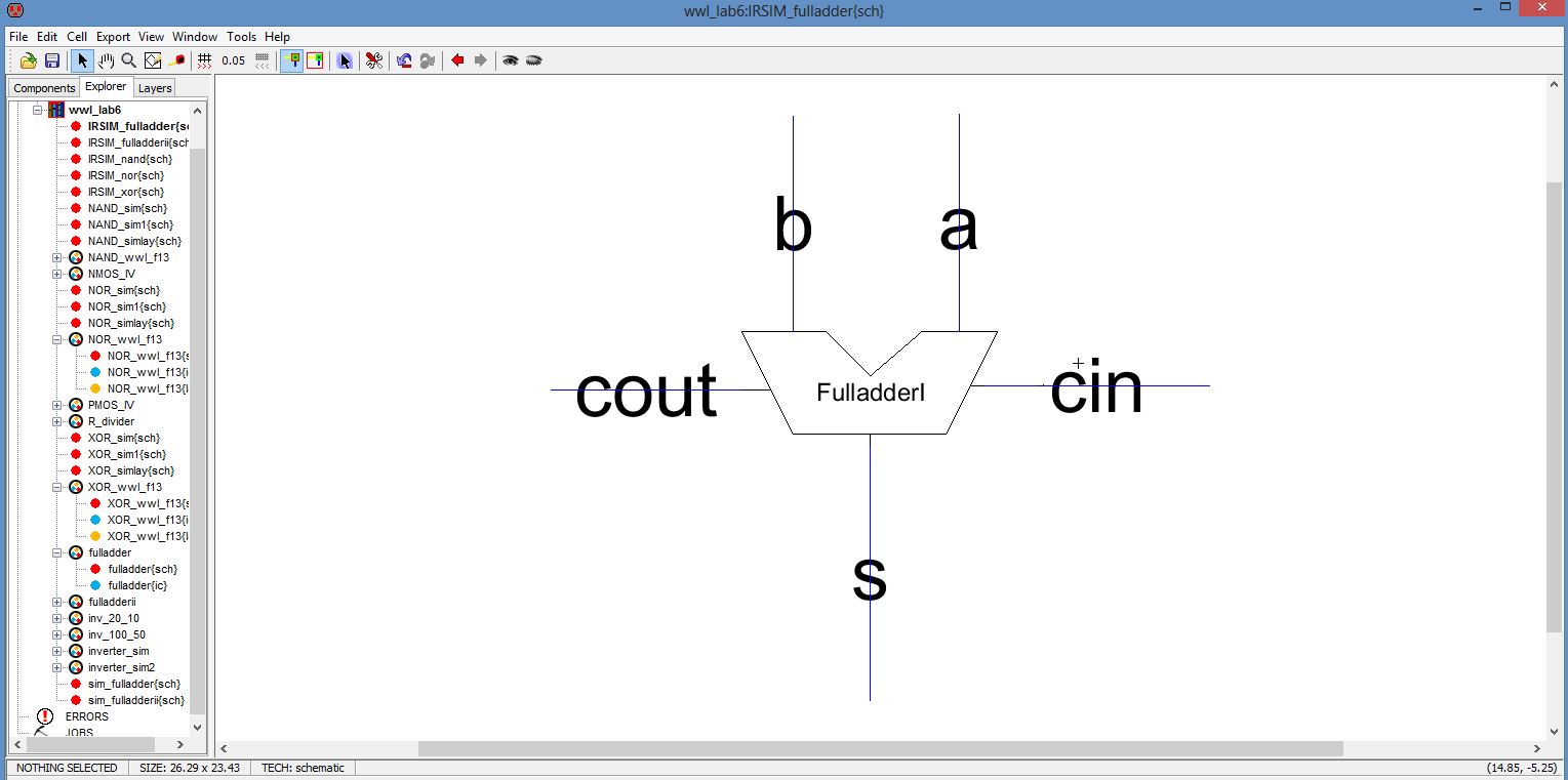
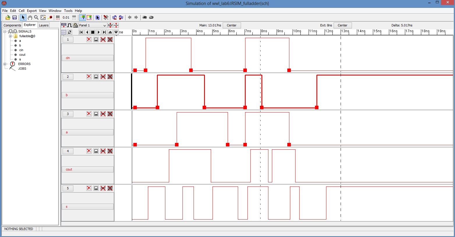
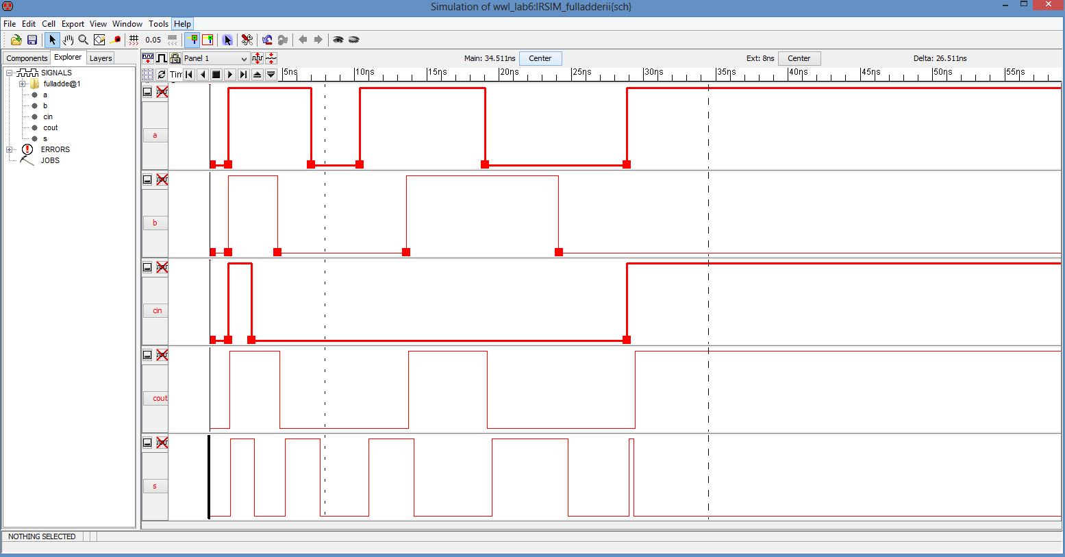
2. For the first full adder, we simulate by LTspice and IRSIM as seen below. I provide 8 different input signals to get the correct outputs.

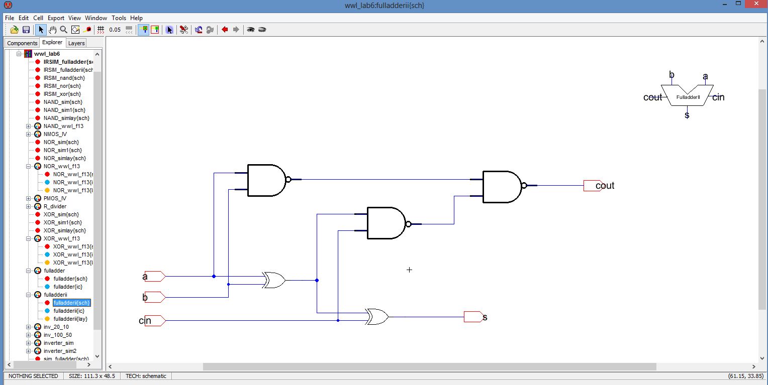
3. Next, design the second full adder with 3 NAND gates and 2 XOR gates. The schematic is shown in the following.
4. The layout design is much more complicated. Pass DRC, NCC, ERC checking.

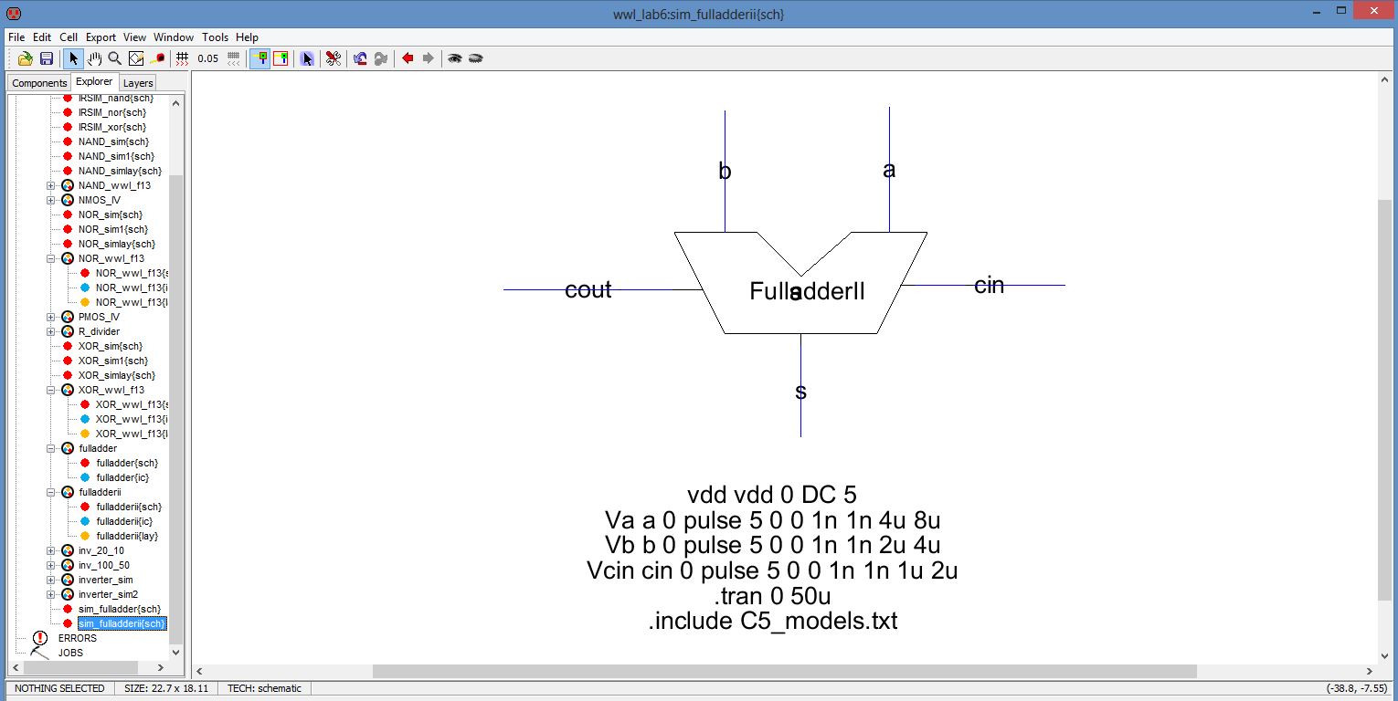
5. The LTspice and IRSIM is shown as below. The spice code is the same as the first full adder.


Backup the work directory for future study