Lab 2 - ECE 421L
Detailed lab-process and discussions with captrued images
Pre-lab part:
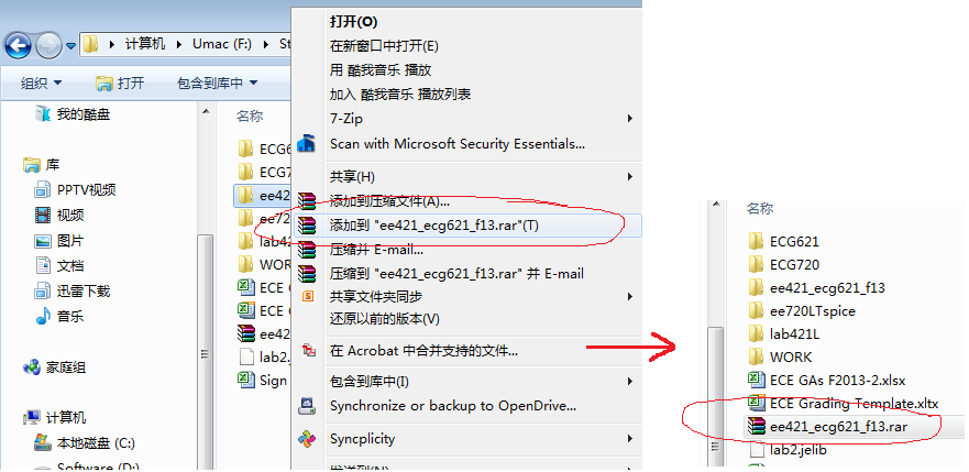
1. Download two library ee421_ecg621.jelib and lab2.jelib. And then use Electric to open both. Then in the left Explorer, we can see two libraries like this
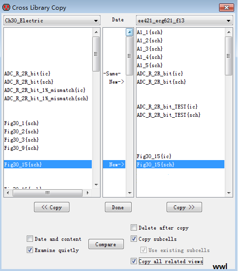
2. Click menu Cell--> Cross-Library Copy.., and we can see the details in both libraries in the open window. And make sure the window like the following highlights with red circle. Then copy sim_ADC_DAC{sch}, all of its subcells, and all related views into ee421_ecg621.jelib. Finally, hit "Done" and close the lab2.jelib in Electric's Explorer. Don't forget backup your library at this time.
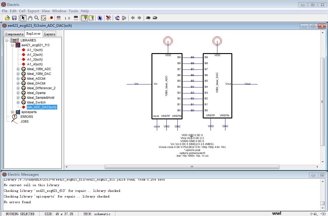
3. Open the sim_ADC_DAC(sch) cell shown like the following image.
4.
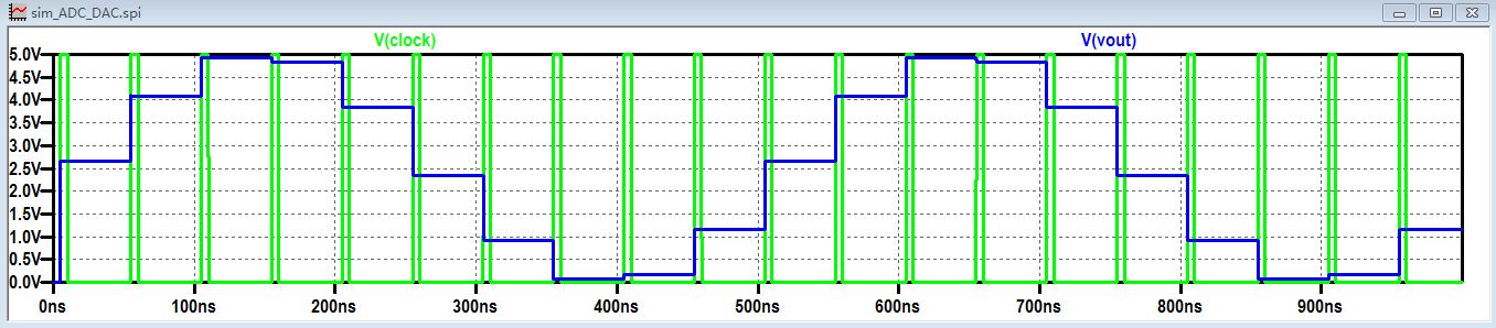
Click F5 to check Hierarchically. And use the shortcut "s"(Tools-->Simulation(Spice)--> Write Spice Deck) to run the
simulation(make sure you have import the electricPrefs.xml). Then we can get the Vin & Vout signal like the
following.

5. ADC aims to convert analog signals or continue signals into digital signals or discrete signals. DAC performs the reverse function. ADC first samples the analog signal and then hold it to convert to digital codes. Next DAC converts the digital codes back into an analog signal, which doesn't change until the next output. Therefore, we can see the above Vout are step signal. Ifwe use different simpling frequency, the width step will be longer or shorter. Fig.(a) is the clock frequency=1/50ns, Fig.(b) is the clock frequency=1/100ns. Due to the second one has a longer holding time, so the DAC output has a longer width.
6. The least significant bit, namely LSB, represents the minumum voltage change on the ADC topology. In the contrary, the most significatn bit (MSB) refers to the leftmost bit of the digital output. 1LSB=Vref/2^N(N is the resolution of ADC.).That means, assuming the reference voltage is the same, 5V, 10-b ADC has 4.88mV LSB value. However, 4-b ADC has 313.5mV LSB value. In other words, the minumum height of step is smaller when resolution is higher. The following two figures prove the above discussions.
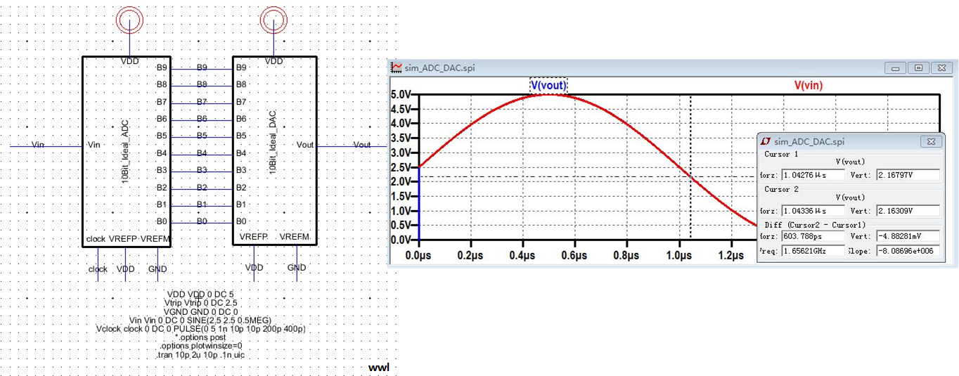
(c) schematic model with simulation result in a 10-b ADC/DAC

(d) schematic model with simulation result in a 4-b ADC/DAC
7. Finish this part. Let's backup.
10-B R-2R DAC Design Part:
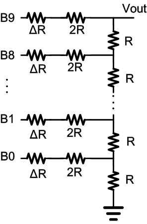
1. In order to quick design a R-2R DAC circuit, go to CMOSedu.com and find out the Electric example of the CMOS Circuit Design, Layout and Simulation Book. Then Open the Chapter 30 Library and ee421_ecg621.jelib. And then use the Cross-Library Copy command to get the Figure30_15 cell and subcells.
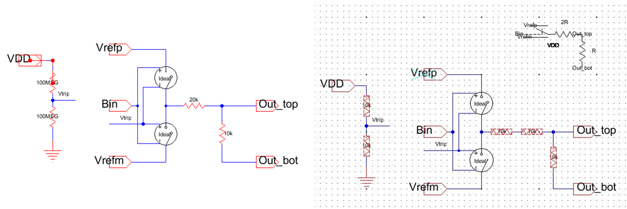
2. Use Ctrl+d to go down the R-2R switch model so we can get the following left figure. Lab2 uses n-well R of 10k. So we need to change the resistor like right figure.
3. Use Ctrl+u to go up to the R-2R DAC model. Delete the spice code and the output capacitor. Follow the Electric tutorial_3 to make a circuit symbol(here it is called icon.). Firstly, add B9-B0, VDD, Vout pins in the correct position. Click View-->Make Icon View so you can see a icon besides the schematic. Click the icon and use Ctrl+D to go down the icon to design the icon. You can use the square in the component or copy from the ideal_10bDAC model. Then you can get a new cell Figure31_15(ic) in the Explorer and the following images will be received.

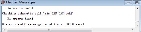
4. Hit F5 or use Tools -> DRC -> Check Hierarchically to check the circuit. Usually, you will get some errors and warnings. At this time, check the circuit and wire connnection. And also you can revmove extra pins using Edit -> Cleanup Cell -> Cleanup Pins Everywhere. Finally, you can get zero error and warning showing in Electric Message window.

5. In order to dertermine the output resistance of the DAC, we assume B0-B9 are connected to gnd, then combine all the parallel and series resistance and get the answer is R.

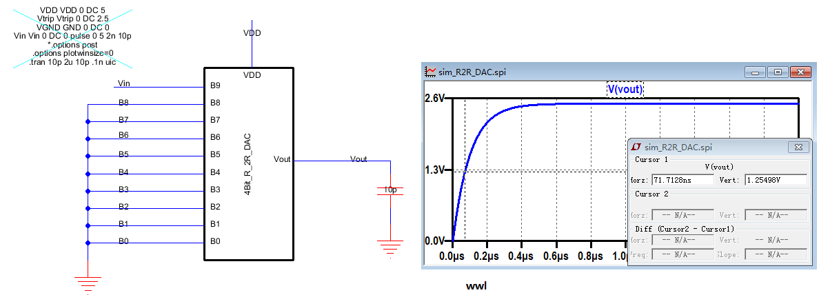
6. Open a new cell called sim_R2R_DAC and Click n to insert the DAC schematic icon. Press "new instance & close" to put the DAC icon in the new cell.

7. Gournd all DAC inputs and give a pulse source Vin (0 to 5V) to B9 node. As we know, the peak voltage of Vout is 2.5V. Use a 10pF capacitor as the load, we can calculate the delay of DAC is 0.7RC=0.07us=70ns. The simulation result in following image proves the calculation.
8. Copy the cell sim_ADC_DAC{sch} to a cell sim2_ADC_DAC{sch}. Use the R-2R DAC to replace the ideal DAC.

9. Then, we add a resistor load to the output. The schematic model and simulation result is shown in the following.
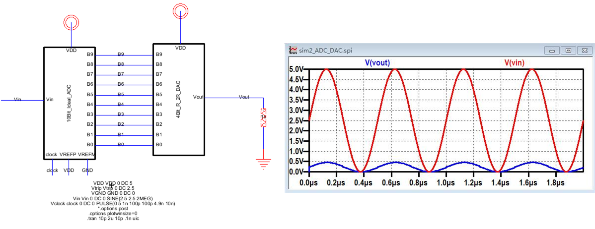
10. Then, we add a capacitor load to the output. The schematic model and simulation result is shown in the following.
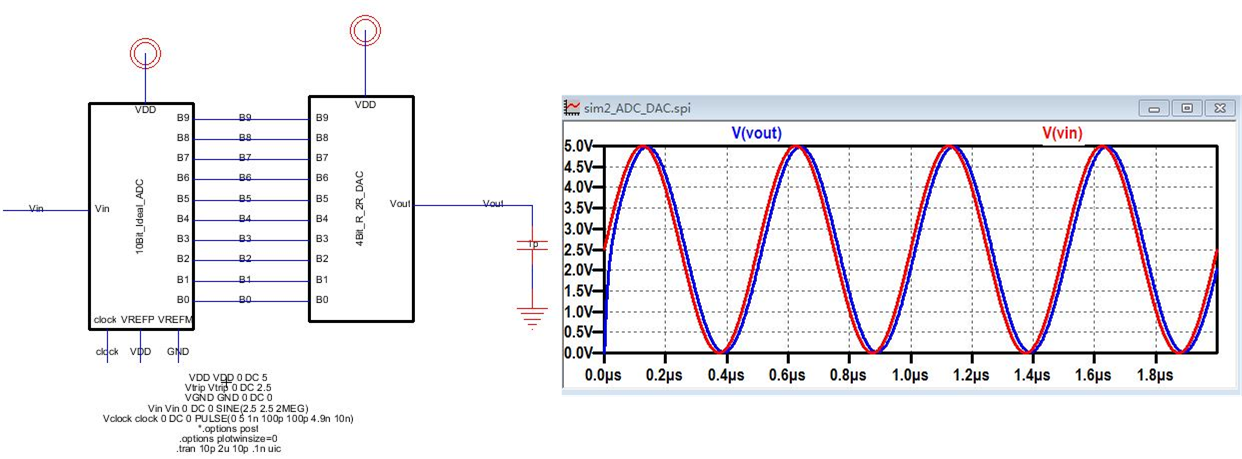
11. Then, we add both resistor and capacitor load to the output. The schematic model and simulation result is shown in the following.
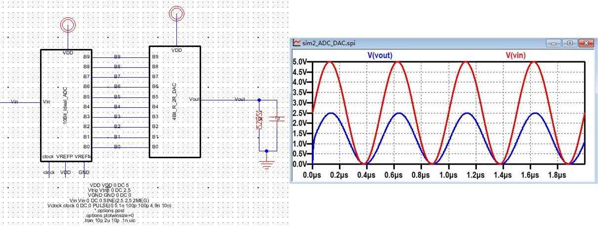
12. If the load is only one resistor, 10k, only the amplitude will be half of the input signal. Because output resistance is R, 10k.

13. In the real circuit, the switches will use transistors. Due to the transistor has parasitic resistance, therefore, each 2R should plus the parasitic resistance. The output voltage will go down.
14. Finally, backup lab2 report and work directory for study and discussion in the future.