Lab 7 - EE 421L
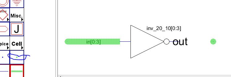
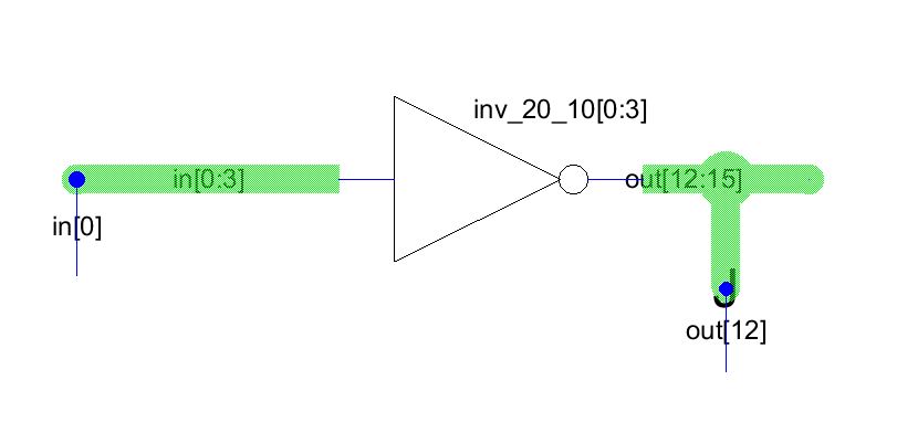
Then go to the component tab and choose the bus symbol, and then right click the other place to make a wire as buses of inputs and outputs. And then put the input/output off-page and connect them to the buses. Don't forget the name the exports as seen below.
Pre-work Tutorial_5:
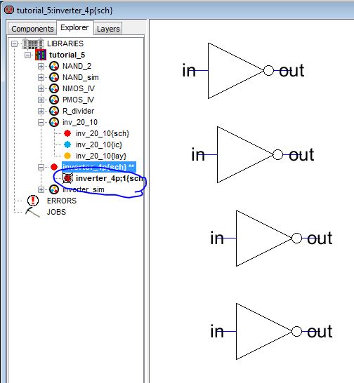
Go through the tutorial_5 learning to use the buses to design the ring oscillator.
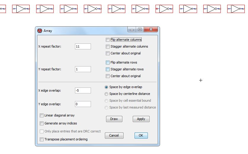
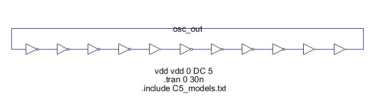
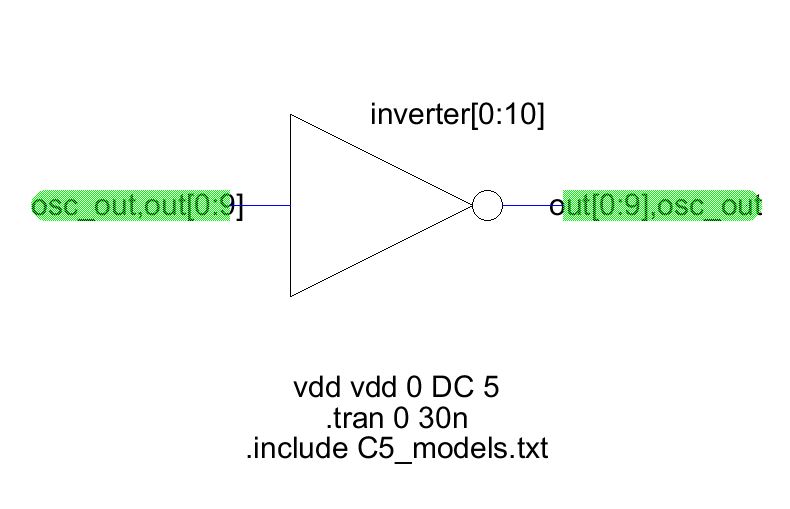
Simulate the ring osillator
LAB7 Design:
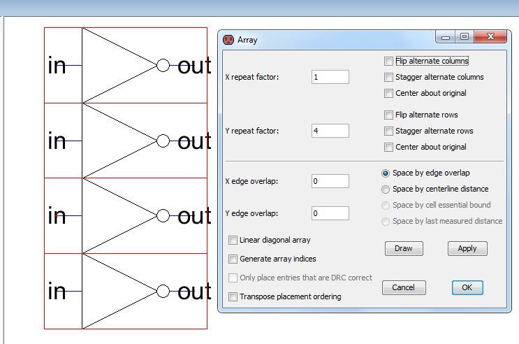
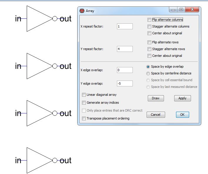
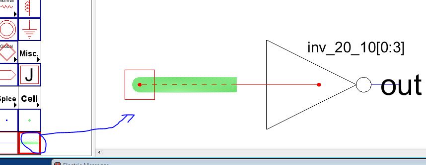
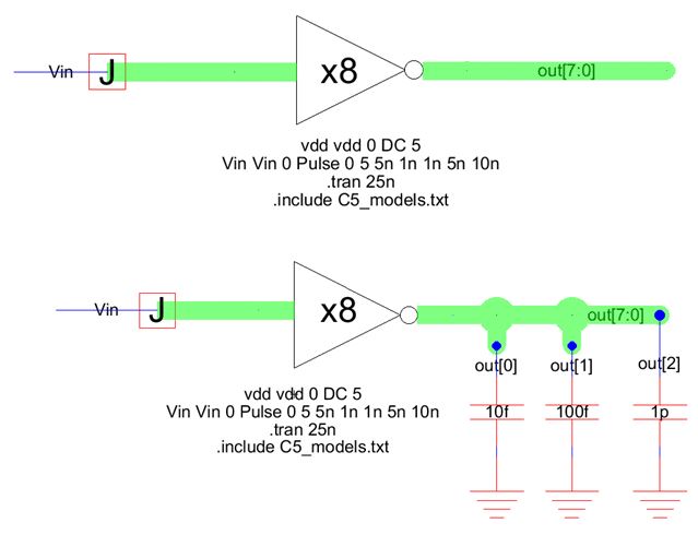
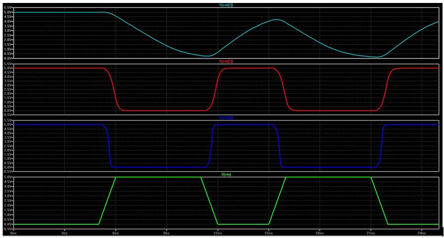
First, make the schematic of a 8-bit inverter, then two different simulation are shown as below. One is without load,
and the other is that several outputs has different capacitive loads.
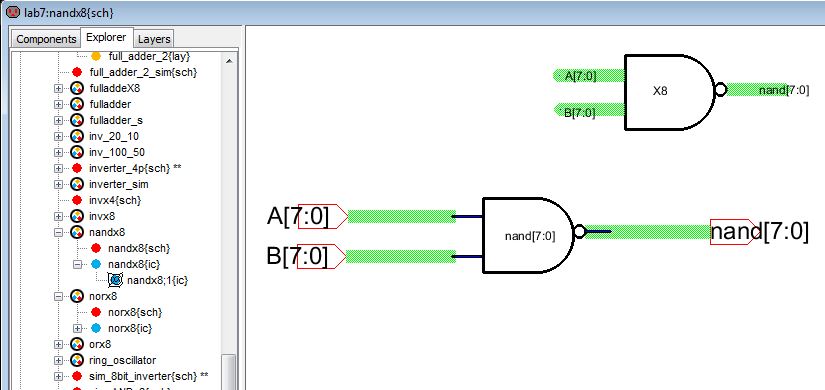
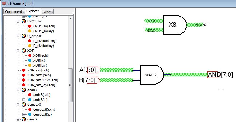
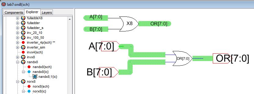
Designning of the 8bit NAND, NOR, AND and OR gates. It is similar as you did in the above invertors.
The NAND GATE
The NOR GATE
The AND GATE
The OR GATE
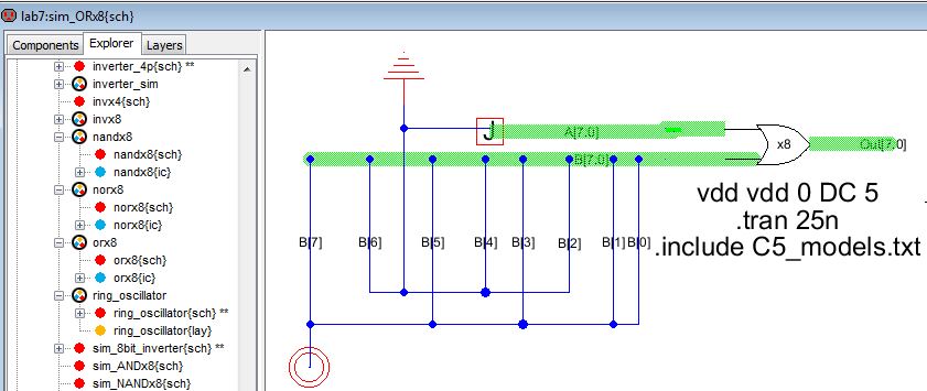
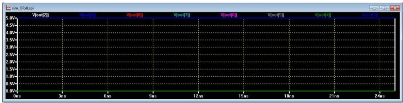
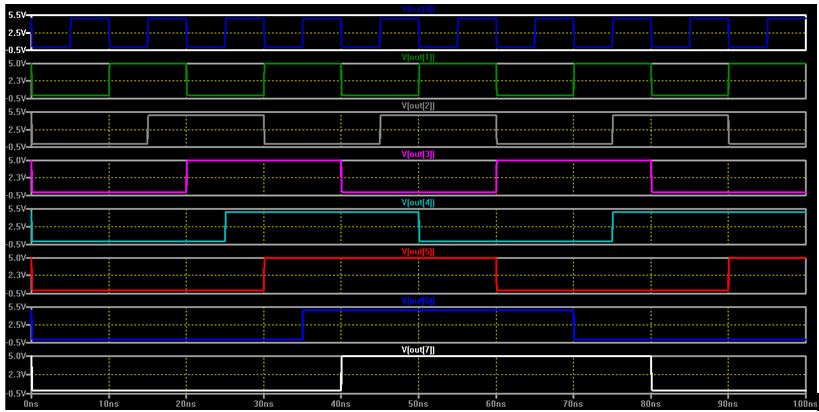
The following fig. is one of the four 8-bit shows how to checking the logic function
they are all similar. Example lets take a look to OR gate
wave form
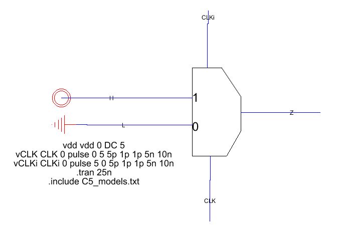
The schematic of 2-to-1 DEMUX. To check the demux function, you can simulate it, and when CLK is high, the A signal (high signal) will be sent to the output.

To design the 8bit demux use bus, then use LTspice and IRSIM to simulate the circuit providing different frequency clock signal and get the different output result.
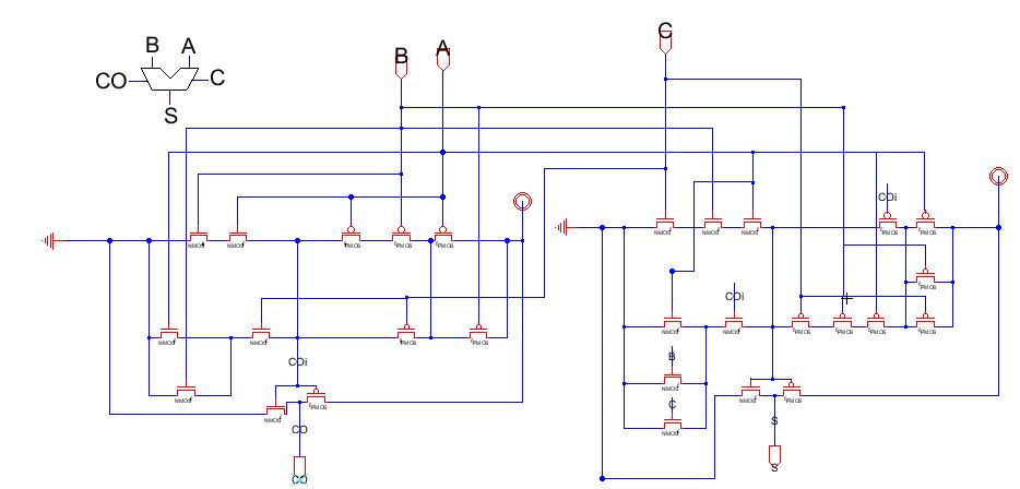
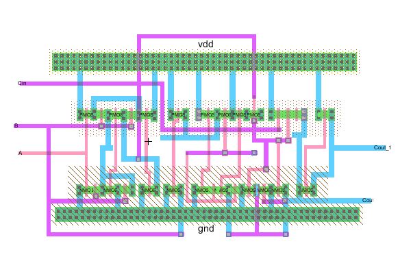
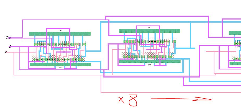
Desgin the high-speed full adder as Fig.12.20 in textbook. W=6, L=2 of the MOSFETs, and
the layout design. And pass DRC, ERC, and NCC.
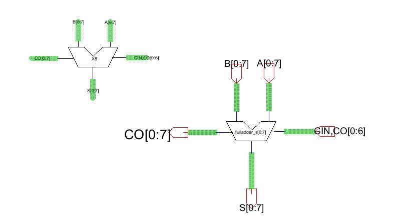
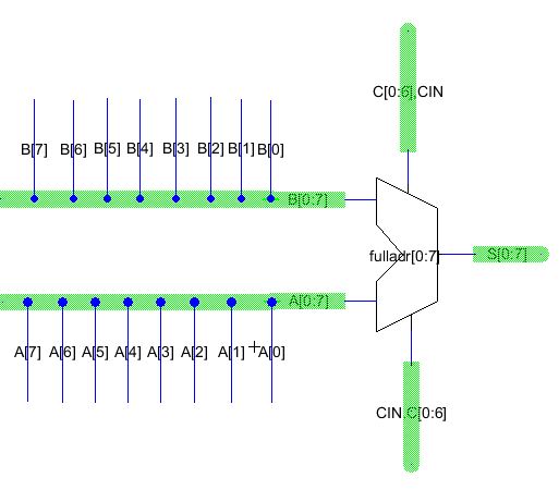
Using buses to design the 8-bit full adder look as following fig.
Then layout, and make sure it pass's DRC, ERC, and NCC.

Backup the work zip it and email it to yourself.

